

Page 1
a
CMOS Sigma-Delta Modulator
AD7720
FEATURES
12.5 MHz Master Clock Frequency
0 V to +2.5 V or 61.25 V Input Range
Single Bit Output Stream
90 dB Dynamic Range
Power Supplies: AVDD, DVDD: +5 V 6 5%
On-Chip 2.5 V Voltage Reference
28-Lead TSSOP
GENERAL DESCRIPTION
This device is a 7th order sigma-delta modulator that converts
the analog input signal into a high speed 1-bit data stream. The
part operates from a +5 V supply and accepts a differential input
range of 0 V to +2.5 V or ± 1.25 V centered about a commonmode bias. The analog input is continuously sampled by the
analog modulator, eliminating the need for external sample and
hold circuitry. The input information is contained in the output
stream as a density of ones. The original information can be
reconstructed with an appropriate digital filter.
The part provides an accurate on-chip 2.5 V reference. A reference input/output function is provided to allow either the internal reference or an external system reference to be used as the
reference source for the part.
The device is offered in a 28-lead TSSOP package and designed
to operate from –40°C to +85°C.
VIN(+)
VIN(–)
MZERO
GC
BIP
STBY
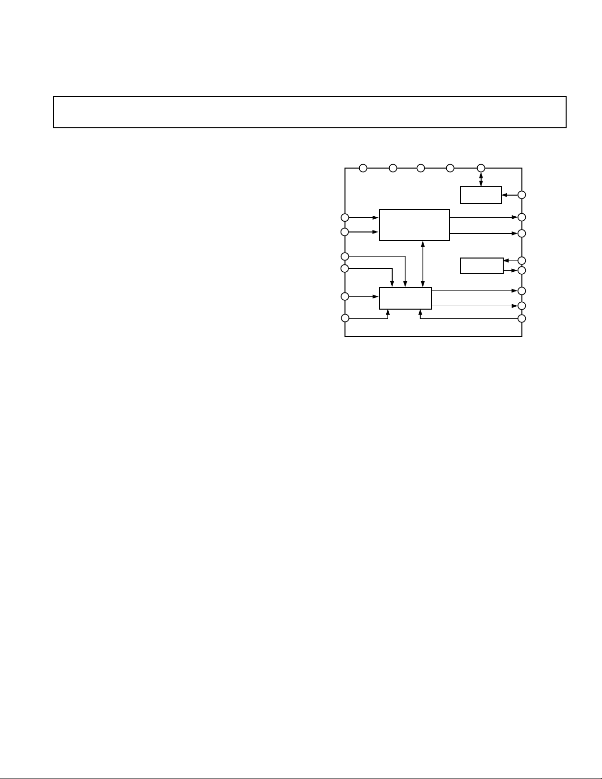
FUNCTIONAL BLOCK DIAGRAM
AVDD AGND DVDD DGND REF1
AD7720
SIGMA-DELTA
MODULATOR
CONTROL
LOGIC
2.5V
REFERENCE
CLOCK
CIRCUITRY
REF2
DATA
SCLK
XTAL1/MCLK
XTAL2
DVAL
RESETO
RESET
REV. 0
Information furnished by Analog Devices is believed to be accurate and
reliable. However, no responsibility is assumed by Analog Devices for its
use, nor for any infringements of patents or other rights of third parties
which may result from its use. No license is granted by implication or
otherwise under any patent or patent rights of Analog Devices.
One Technology Way, P.O. Box 9106, Norwood, MA 02062-9106, U.S.A.
Tel: 781/329-4700 World Wide Web Site: http://www.analog.com
Fax: 781/326-8703 © Analog Devices, Inc., 1997
Page 2

AD7720–SPECIFICA TIONS
(AVDD = +5 V 6 5%; DVDD = +5 V 6 5%; AGND = DGND = 0 V, f
1
REF2 = +2.5 V; TA = T
MIN
to T
, unless otherwise noted)
MIN
= 12.5 MHz,
MCLK
Parameter B Version Units Test Conditions/Comments
STATIC PERFORMANCE When Tested with Ideal FIR Filter as in Figure 1
Resolution 16 Bits
Differential Nonlinearity ±1 LSB max Guaranteed Monotonic
Integral Nonlinearity ±2 LSB typ
Precalibration Offset Error ±6 mV typ
Precalibration Gain Error
Postcalibration Offset Error
Postcalibration Gain Error
2
3
2, 3
±0.6 % FSR typ
±1.5 mV typ
±0.3 % FSR typ
Offset Error Drift ±1 LSB/°C typ
Gain Error Drift REF2 Is an Ideal Reference, REF1 = AGND
Unipolar Mode ±1 LSB/°C typ
Bipolar Mode ±0.5 LSB/°C typ
ANALOG INPUTS
Signal Input Span (VIN(+) – VIN(–))
Bipolar Mode ±V
Unipolar Mode 0 to V
/2 V max BIP = V
REF2
REF2
V max BIP = V
IH
IL
Maximum Input Voltage AVDD V
Minimum Input Voltage 0 V
Input Sampling Capacitance 2 pF typ
Input Sampling Rate 2 f
MCLK
Differential Input Impedance 109/(8 f
MCLK
MHz
)kΩ typ
REFERENCE INPUTS
REF1 Output Voltage 2.32 to 2.62 V min/max
REF1 Output Voltage Drift 60 ppm/°C typ
REF1 Output Impedance 3 kΩ typ
Reference Buffer Offset Voltage ±12 mV max Offset Between REF1 and REF2
Using Internal Reference
REF2 Output Voltage 2.32 to 2.62 V min/max
REF2 Output Voltage Drift 60 ppm/°C typ
Using External Reference REF1 = AGND
REF2 Input Impedance 10
9
/(16 f
MCLK
)kΩ typ
External Reference Voltage Range 2.32 to 2.62 V min/max Applied to REF1 or REF2
DYNAMIC SPECIFICATIONS
Bipolar Mode BIP = V
Signal to (Noise + Distortion)
Total Harmonic Distortion
4
5
5
90 dB typ Input BW = 0 kHz–90.625 kHz
86/84.5 dB min
–90/–88 dB max Input BW = 0 kHz–90.625 kHz
When Tested with Ideal FIR Filter as in Figure 1
, VCM = 2.5 V, VIN(+) = VIN(–) = 1.25 V p-p
IH
or VIN(–) = 1.25 V, VIN(+) = 0 V to 2.5 V
Spurious Free Dynamic Range –90 dB max Input BW = 0 kHz–90.625 kHz
Unipolar Mode BIP = V
Signal to (Noise + Distortion)
Total Harmonic Distortion
5
5
88 dB typ Input BW = 0 kHz–90.625 kHz
84.5/83 dB min
–89/–87 dB max Input BW = 0 kHz–97.65 kHz
, VIN(–) = 0 V, VIN(+) = 0 V to 2.5 V
IL
Spurious Free Dynamic Range –90 dB max Input BW = 0 kHz–97.65 kHz
Intermodulation Distortion –93 dB typ
AC CMRR 96 dB typ VIN(+) = VIN(–) = 2.5 V p-p, V
= 1.25 V to
CM
3.75 V, 20 kHz
Overall Digital Filter Response See Figure 1 for Characteristics of FIR Filter
0 kHz–90.625 kHz ±0.005 dB max
96.92 kHz –3 dB min
104.6875 kHz to 12.395 MHz 90 dB typ
CLOCK
MCLK Duty Ratio 45 to 55 % max For Specified Operation
V
V
, MCLK High Voltage 4 V min MCLK Uses CMOS Logic
MCLKH
, MCLK Low Voltage 0.4 V max
MCLKL
–2–
REV. 0
Page 3
Parameter B Version Units Test Conditions/Comments
LOGIC INPUTS
VIH, Input High Voltage 2 V min
V
, Input Low Voltage 0.8 V max
IL
I
, Input Current 10 µA max
INH
CIN, Input Capacitance 10 pF max
LOGIC OUTPUTS
V
, Output High Voltage 2.4 V min |I
OH
VOL, Output Low Voltage 0.4 V max |I
| ≤ 200 µA
OUT
| ≤ 1.6 mA
OUT
POWER SUPPLIES
AVDD 4.75/5.25 V min/V max
DVDD 4.75/5.25 V min/V max
I
(Total for AVDD, DVDD) Digital Inputs Equal to 0 V or DVDD
DD
Active Mode 43 mA max
Standby Mode 25 µA max
NOTES
1
Operating temperature range is as follows: B Version: –40°C to +85°C.
2
Gain Error excludes reference error. The modulator gain is calibrated w.r.t. the voltage on the REF2 pin.
3
Applies after calibration at temperature of interest.
4
Measurement Bandwidth = 0.5 × f
5
TA = +25°C to +85°C/TA = T
Specifications subject to change without notice.
; Input Level = –0.05 dB.
MCLK
to T
MAX
.
MIN
AD7720
BIT STREAM
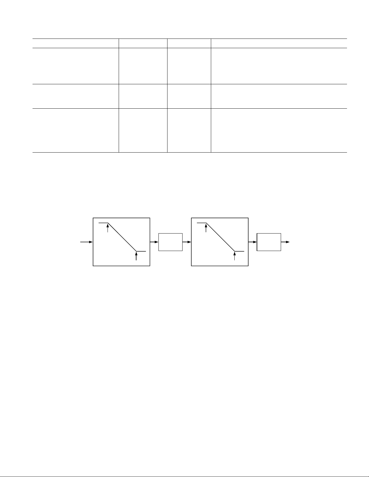
90.625kHz
FILTER 1
BANDWIDTH = 90.625 kHz
TRANSITION = 292.969kHz
ATTENUATION = 120dB
COEFFICIENTS = 384
292.969kHz
120dB
DECIMATE
BY 32
90.625kHz
FILTER 2
BANDWIDTH = 90.625 kHz
TRANSITION = 104.687kHz
ATTENUATION = 90dB
COEFFICIENTS = 151
104.687kHz
90dB
DECIMATE
BY 2
16-BIT
OUTPUT
Figure 1. Digital Filter (Consists of 2 FIR Filters). This filter is implemented on the AD7722.
–3–REV. 0
Page 4
AD7720
TIMING CHARACTERISTICS
Limit at T
(AVDD = +5 V 6 5%; DVDD = +5 V 6 5%; AGND = DGND = 0 V, REF2= +2.5 V unless otherwise noted)
, T
MIN
MAX
Parameter (B Version) Units Conditions/Comments
f
MCLK
100 kHz min Master Clock Frequency
15 MHz max 12.5 MHz for Specified Performance
t
1
t
2
t
3
t
4
t
5
t
6
t
7
NOTE
Guaranteed by design.
67 ns min Master Clock Period
0.45 × t
0.45 × t
MCLK
MCLK
ns min Master Clock Input High Time
ns min Master Clock Input Low Time
15 ns min Data Hold Time After SCLK Rising Edge
10 ns min RESET Pulsewidth
10 ns min RESET Low Time Before MCLK Rising
20 × t
MCLK
OUTPUT
ns max DVAL High Delay after RESET Low
I
OL
1.6mA
PIN
TO
50pF
C
L
I
OH
200 A
+1.6V
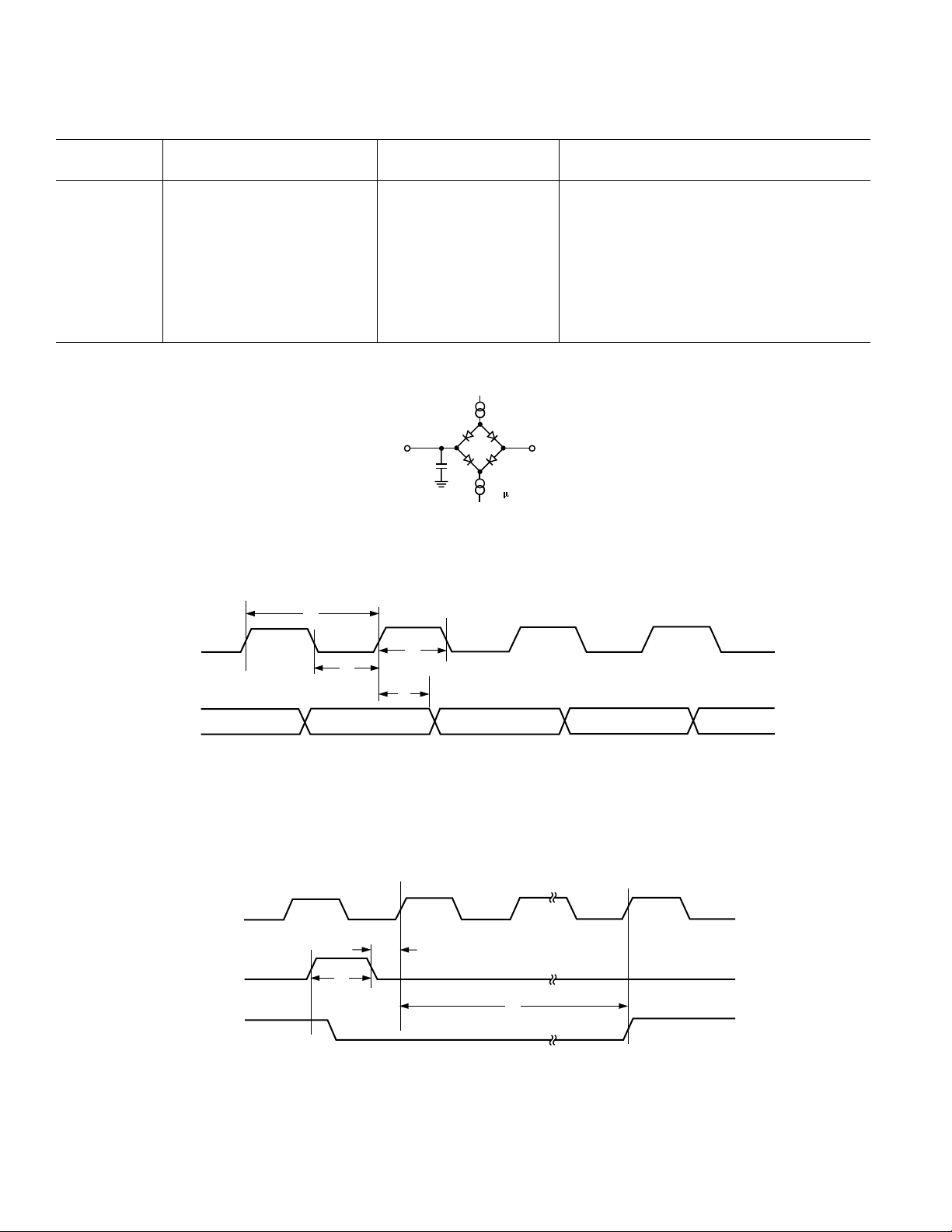
Figure 2. Load Circuit for Access Time and Bus Relinquish Time
SCLK (O)
DATA (O)
NOTE:
O SIGNIFIES AN OUTPUT
MCLK (I)
RESET (I)
DVAL (O)
t
1
t
t
3
2
t
4
Figure 3. Data Timing
t
6
t
5
t
7
NOTE:
I SIGNIFIES AN INPUT
O SIGNIFIES AN OUTPUT
Figure 4. RESET Timing
–4–
REV. 0
Page 5
AD7720
ABSOLUTE MAXIMUM RATINGS
1
(TA = +25°C unless otherwise noted)
DVDD to DGND . . . . . . . . . . . . . . . . . . . . . . –0.3 V to +7 V
AVDD to AGND . . . . . . . . . . . . . . . . . . . . . . –0.3 V to +7 V
AVDD to DVDD . . . . . . . . . . . . . . . . . . . . –0.3 V to +0.3 V
AGND to DGND . . . . . . . . . . . . . . . . . . . . –0.3 V to +0.3 V
Digital Input Voltage to DGND . . –0.3 V to DVDD + 0.3 V
Analog Input Voltage to AGND . . . –0.3 V to AVDD + 0.3 V
Input Current to Any Pin Except Supplies
2
. . . . . . . ±10 mA
Operating Temperature Range
Industrial (B Version) . . . . . . . . . . . . . . . –40°C to +85°C
Storage Temperature Range . . . . . . . . . . . . –65°C to +150°C
Maximum Junction Temperature . . . . . . . . . . . . . . . +150°C
TSSOP Package
θ
Thermal Impedance . . . . . . . . . . . . . . . . . . . . 120°C/W
JA
Lead Temperature, Soldering
Vapor Phase (60 sec) . . . . . . . . . . . . . . . . . . . . . +215°C
Infrared (15 sec) . . . . . . . . . . . . . . . . . . . . . . . . . +220°C
NOTES
1
Stresses above those listed under Absolute Maximum Ratings may cause perma-
nent damage to the device. This is a stress rating only; functional operation of the
device at these or any other conditions above those listed in the operational
sections of this specification is not implied. Exposure to absolute maximum rating
conditions for extended periods may affect device reliability.
2
Transient currents of up to 100 mA will not cause SCR latchup.
PIN CONFIGURATION
REF2
AGND
NC
STBY
DVAL
DGND
GC
BIP
MZERO
DATA
SCLK
RESETO
NC
AGND
1
2
3
4
5
6
AD7720
7
TOP VIEW
(Not to Scale)
8
9
10
11
12
13
14
NC = NO CONNECT
28
AVDD
27
REF1
26
AGND
25
AVDD
24
AGND
VIN(+)
23
22
RESET
21
VIN(–)
20
AGND
19
DVDD
18
AGND
17
XTAL2
16
XTAL1/MCLK
15
DGND
ORDERING GUIDE
Temperature Package Package
Model Range Description Option
AD7720BRU –40°C to +85°C 28-Lead Thin Shrink Small Outline RU-28
CAUTION
ESD (electrostatic discharge) sensitive device. Electrostatic charges as high as 4000 V readily
accumulate on the human body and test equipment and can discharge without detection.
Although the AD7720 features proprietary ESD protection circuitry, permanent damage may
occur on devices subjected to high energy electrostatic discharges. Therefore, proper ESD
precautions are recommended to avoid performance degradation or loss of functionality.
WARNING!
ESD SENSITIVE DEVICE
–5–REV. 0
Page 6

AD7720
PIN FUNCTION DESCRIPTIONS
Pin No. Mnemonic Function
1 REF2 Reference Input/Output. REF2 connects to the output of an internal buffer amplifier used
to drive the sigma-delta modulator. When REF2 is used as an input, REF1 must be con-
nected to AGND.
2, 14, 18, 20, 24, 26 AGND Ground reference point for analog circuitry.
3, 13 NC No Connect.
4 STBY Standby, Logic Input. When STBY is high, the device is placed in a low power mode.
When STBY is low, the device is powered up.
5 DVAL Data Valid Logic Output. A logic high on DVAL indicates that the data bit stream from
the AD7720 is an accurate digital representation of the analog voltage at the input to the
sigma-delta modulator. The DVAL pin is set low for 20 MCLK cycles if the analog input is
overranged.
6, 15 DGND Ground reference for the digital circuitry.
7 GC Digital Control Input. When GC is high, the gain error of the modulator can be calibrated.
8 BIP Analog Input Range Select, Logic Input. A logic low on this input selects unipolar mode. A
logic high selects bipolar mode.
9 MZERO Digital Control Input. When MZERO is high, the modulator inputs are internally grounded,
i.e., tied to AGND in unipolar mode and REF2 in bipolar mode. MZERO allows on-chip
offsets to be calibrated out. MZERO is low for normal operation.
10 DATA Modulator Bit Stream. The digital bit stream from the sigma-delta modulator is output at
DATA.
11 SCLK Serial Clock, Logic Output. The bit stream from the modulator is valid on the rising edge
of SCLK.
12 RESETO Reset Logic Output. The signal applied to the RESET pin is made available as an output at
RESETO.
16 XTAL1/MCLK CMOS Logic Clock Input. The XTAL1/MCLK pin interfaces the device’s internal oscillator
circuit to an external crystal or an external clock. A parallel resonant, fundamental-frequency,
microprocessor-grade crystal and a 1 MΩ resistor should be connected between the MCLK
and XTAL pins with two capacitors connected from each pin to ground. Alternatively, the
XTAL1/MCLK pin can be driven with an external CMOS-compatible clock. The part is
specified with a 12.5 MHz master clock.
17 XTAL2 Oscillator Output. The XTAL2 pin connects the internal oscillator output to an external
crystal. If an external clock is used, XTAL2 should be left unconnected.
19 DVDD Digital Supply Voltage, +5 V ± 5%.
21, 23 VIN(–), VIN(+) Analog Input. In unipolar operation, the analog input range on VIN(+) is VIN(–) to
(VIN(–) + V
The absolute analog input range must lie between 0 and AVDD. The analog input is con-
tinuously sampled and processed by the analog modulator.
25, 28 AVDD Analog Positive Supply Voltage, +5 V ± 5%.
22 RESET Reset Logic Input. RESET is an asynchronous input. When RESET is taken high, the
sigma-delta modulator is reset by shorting the integrator capacitors in the modulator. DVAL
goes low for 20 MCLK cycles while the modulator is being reset.
27 REF1 Reference Input/Output. REF1 connects via a 3 kΩ resistor to the output of the internal
2.5 V reference, and to the input of a buffer amplifier that drives the sigma-delta modulator.
This pin can also be overdriven with an external 2.5 V reference.
); for bipolar operation, the analog input range on VIN+ is (VIN(–) ± V
REF
REF
/2).
–6–
REV. 0
Page 7

AD7720
TERMINOLOGY (IDEAL FIR FILTER USED WITH AD7720
[FIGURE 1])
Integral Nonlinearity
This is the maximum deviation of any code from a straight line
passing through the endpoints of the transfer function. The
endpoints of the transfer function are zero scale (not to be confused with bipolar zero), a point 0.5 LSB below the first code
transition (100...00 to 100...01 in bipolar mode and
000...00 to 000...01 in unipolar mode) and full scale, a
point 0.5 LSB above the last code transition (011...10 to
011...11 in bipolar mode and 111...10 to 111...11 in
unipolar mode). The error is expressed in LSBs.
Differential Nonlinearity
This is the difference between the measured and the ideal 1 LSB
change between two adjacent codes in the ADC.
Common-Mode Rejection Ratio
The ability of a device to reject the effect of a voltage applied to
both input terminals simultaneously—often through variation of
a ground level—is specified as a common-mode rejection ratio.
CMRR is the ratio of gain for the differential signal to the gain
for the common-mode signal.
Unipolar Offset Error
Unipolar offset error is the deviation of the first code transition
from the ideal VIN(+) voltage which is (VIN(–) + 0.5 LSB)
when operating in the unipolar mode.
Bipolar Offset Error
This is the deviation of the midscale transition (111...11
to 000...00) from the ideal VIN(+) voltage which is (VIN(–)
–0.5 LSB) when operating in the bipolar mode.
Gain Error
The first code transition should occur at an analog value 1/2
LSB above minus full scale. The last code transition should
occur for an analog value 3/2 LSB below the nominal full scale.
Gain error is the deviation of the actual difference between first
and last code transitions and the ideal difference between first
and last code transitions.
Signal-to-(Noise + Distortion)
Signal-to-(Noise + Distortion) is measured signal-to-noise at the
output of the ADC. The signal is the rms magnitude of the
fundamental. Noise plus distortion is the rms sum of all of the
nonfundamental signals and harmonics to half the output word
rate (f
/128), excluding dc. Signal-to-(Noise + Distortion) is
MCLK
dependent on the number of quantization levels used in the
digitization process; the more levels, the smaller the quantization noise. The theoretical Signal-to-(Noise + Distortion) ratio
for a sine wave input is given by
Signal-to-(Noise + Distortion) = (6.02 N + 1.76) dB
where N is the number of bits.
Total Harmonic Distortion
Total Harmonic Distortion (THD) is the ratio of the rms sum
of harmonics to the rms value of the fundamental. For the
AD7720, THD is defined as
2
2
2
2
2
+V
)
5
6
THD = 20 log
(V
+V
+V
2
+V
3
4
V
1
where V1 is the rms amplitude of the fundamental and V2, V3,
V
, V5 and V6 are the rms amplitudes of the second through the
4
sixth harmonic.
Spurious Free Dynamic Range
Spurious free dynamic range is the difference, in dB, between
the peak spurious or harmonic component in the ADC output
spectrum (up to f
/128 and excluding dc) and the rms value
MCLK
of the fundamental. Normally, the value of this specification will
be determined by the largest harmonic in the output spectrum
of the FFT. For input signals whose second harmonics occur in
the stop band region of the digital filter, a spur in the noise floor
limits the spurious free dynamic range.
Intermodulation Distortion
With inputs consisting of sine waves at two frequencies, fa and
fb, any active device with nonlinearities will create distortion
products at sum and difference frequencies of mfa ± nfb where
m, n = 0, 1, 2, 3, etc. Intermodulation distortion terms are
those for which neither m or n are equal to zero. For example,
the second order terms include (fa + fb) and (fa – fb), while the
third order terms include (2fa + fb), (2fa – fb), (fa + 2fb) and
(fa – 2fb).
–7–REV. 0
Page 8

AD7720–Typical Characteristics
(AVDD = DVDD = 5.0 V, TA = +258C; CLKIN = 12.5 MHz, AIN = 20 kHz, Bipolar Mode; VIN(+) = 0 V to 2.5 V, VIN(–) = 1.25 V unless otherwise
noted)
110
100
90
80
dB
70
60
50
–40 –30 0
SFDR
S/ (N+D)
–20 –10
INPUT LEVEL – dB
Figure 5. S/(N+D) and SFDR vs.
Analog Input Level
–85
–90
SNR
–95
THD
–100
dB
–105
SFDR
–110
–115
0 20 100
VIN (+) = VIN(–) = 1.25Vpk–pk
V
= 2.5V
CM
40 60 80
INPUT FREQUENCY – kHz
84
85
AIN = 1/5 · BW
86
87
88
dB
89
90
91
92
0 50 300
100 150 200 250
OUTPUT DATA RATE – kSPS
Figure 6. S/(N+D) vs. Output Sample
Rate
84
85
AIN = 1/5 · BW
VIN (+) = VIN(–) = 1.25Vpk–pk
86
V
= 2.5V
CM
87
88
dB
89
90
91
92
0 50 300
100 150 200 250
OUTPUT DATA RATE – kSPS
–85
–90
–95
–100
dB
–105
–110
–115
0 20 100
SNR
SFDR
THD
40 60 80
INPUT FREQUENCY – kHz
Figure 7. SNR, THD, and SFDR vs.
Input Frequency
92.0
91.5
91.0
90.5
90.0
dB
89.5
89.0
88.5
88.0
–50 0 100
TEMPERATURE – °C
50
Figure 8. SNR, THD, and SFDR vs.
Input Frequency
–94
–96
–98
–100
–102
–104
dB
–106
–108
–110
–112
–114
–116
–50 –25 100
THD
0255075
TEMPERATURE – °C
3RD
4TH
2ND
Figure 11. THD vs. Temperature
Figure 9. S/(N+D) vs. Output Sample
Rate
5000
4500
4000
3500
3000
2500
2000
1500
1000
FREQUENCY OF OCCURENCE
500
0
n–3 n–2 n+3
VIN(+) = VIN(–)
CLKIN = 12.5MHz
8k SAMPLES
n–1 n n+1 n+2
CODES
Figure 12. Histogram of Output Codes
with DC Input
Figure 10. SNR vs. Temperature
1.0
0.8
0.6
0.4
0.2
0
–0.2
–0.4
DNL ERROR – LSB
–0.6
–0.8
–1.0
0 20000 6553540000
CODE
Figure 13. Differential Nonlinearity
–8–
REV. 0
Page 9

0
0
1.0
0.8
0.6
0.4
0.2
0
–0.2
INL ERROR – LSB
–0.4
–0.6
–0.8
–1.0
0 20000 6553540000
CODE
Figure 14. Integral Nonlinearity Error
AD7720
0
–10
–20
–30
–40
–50
–60
dB
–70
–80
–90
–100
–110
–120
–130
0 6.25
FREQUENCY – MHz
Figure 15. Modulator Output (0 Hz to MCLK/2)
0
–20
–40
–60
–80
dB
–100
–120
–140
–154
0E+0 10E+3 20E+3 30E+3 40E+3 50E+3 60E+3 70E+3 80E+3
CLKIN = 12.5MHz
SNR = 90.1dB
S/(N+D) = 89.2dB
SFDR = –99.5dB
THD = –96.6dB
2ND = –100.9dB
3RD = –106.0dB
4TH = –99.5dB
90E+3
98E+3
0
–10
–20
–30
–40
–50
–60
dB
–70
–80
–90
–100
–110
–120
–130
0
FREQUENCY – kHz
Figure 18. Modulator Output (0 to 393.295 kHz)
AIN = 90kHz
–20
CLKIN = 12.5 MHz
SNR = 89.6dB
–40
S/(N+D) = 89.6dB
SFDR = –108.0dB
–60
–80
dB
–100
–120
–140
–154
0E+0 10E+3 20E+3 30E+3 40E+3 50E+3 60E+3 70E+3 80E+3 98E+3
90E+3
393.295 kHz
Figure 16. 16K Point FFT
0
–20
–40
–60
–80
dB
–100
–120
–140
–154
0E+0 10E+3 20E+3 30E+3 40E+3 50E+3 60E+3 70E+3 80E+3 96E+3
XTAL = 12.288MHz
SNR = 89.0dB
S/(N+D) = 87.8dB
SFDR = –94.3dB
THD = –93.8dB
2ND = –94.3dB
3RD = –108.5dB
4TH = –105.7dB
dB
90E+3
AIN = 90kHz
–20
XTAL = 12.288MHz
SNR = 88.1dB
–40
S/(N+D) = 88.1dB
SFDR = –103.7dB
–60
–80
–100
–120
–140
–154
0E+0 10E+3 20E+3 30E+3 40E+3 50E+3 60E+3 70E+3 80E+3 96E+3
Figure 17. 16K Point FFT
Figure 19. 16K Point FFT
90E+3
Figure 20. 16K Point FFT
–9–REV. 0
Page 10

AD7720
CIRCUIT DESCRIPTION
Sigma-Delta ADC
The AD7720 ADC employs a sigma-delta conversion technique
that converts the analog input into a digital pulse train. The
analog input is continuously sampled by a switched capacitor
modulator at twice the rate of the clock input frequency (2 ×
f
). The digital data that represents the analog input is in
MCLK
the one’s density of the bit stream at the output of the sigmadelta modulator. The modulator outputs the bit stream at a data
rate equal to f
MCLK
.
Due to the high oversampling rate, which spreads the quantization noise from 0 to f
/2, the noise energy contained in the
MCLK
band of interest is reduced (Figure 21a). To reduce the quantization noise further, a high order modulator is employed to
shape the noise spectrum, so that most of the noise energy is
shifted out of the band of interest (Figure 21b).
QUANTIZATION NOISE
f
/2
BAND OF INTEREST
MCLK
a.
NOISE SHAPING
f
/2
BAND OF INTEREST
MCLK
b.
Figure 21. Sigma-Delta ADC
USING THE AD7720
ADC Differential Inputs
The AD7720 uses differential inputs to provide common-mode
noise rejection (i.e., the converted result will correspond to the
differential voltage between the two inputs). The absolute voltage on both inputs must lie between AGND and AVDD.
In the unipolar mode, the full-scale input range (VIN(+) –
VIN(–)) is 0 V to V
full-scale analog input range is ±V
. In the bipolar mode configuration, the
REF
/2. The bipolar mode
REF2
allows complementary input signals. Alternatively, VIN(–) can
be connected to a dc bias voltage to allow a single-ended input
on VIN(+) equal to V
BIAS
± V
REF2
/2.
Differential Inputs
The analog input to the modulator is a switched capacitor design. The analog input is converted into charge by highly linear
sampling capacitors. A simplified equivalent circuit diagram of
the analog input is shown in Figure 22. A signal source driving
the analog input must be able to provide the charge onto the
sampling capacitors every half MCLK cycle and settle to the
required accuracy within the next half cycle.
A
B
A
B
A
2pF
2pF
AC
GROUND
A
B
B
VIN(+)
VIN(–)
500
500
MCLK
Figure 22. Analog Input Equivalent Circuit
Since the AD7720 samples the differential voltage across its
analog inputs, low noise performance is attained with an input
circuit that provides low differential mode noise at each input.
The amplifiers used to drive the analog inputs play a critical
role in attaining the high performance available from the AD7720.
When a capacitive load is switched onto the output of an op
amp, the amplitude will momentarily drop. The op amp will try
to correct the situation and, in the process, hits its slew rate
limit. This nonlinear response, which can cause excessive ringing, can lead to distortion. To remedy the situation, a low pass
RC filter can be connected between the amplifier and the input
to the AD7720 as shown in Figure 23. The external capacitor
at each input aids in supplying the current spikes created during
the sampling process. The resistor in this diagram, as well as
creating the pole for the antialiasing, isolates the op amp from
the transient nature of the load.
ANALOG
INPUT
R
C
R
C
VIN(+)
VIN(–)
Figure 23. Simple RC Antialiasing Circuit
The differential input impedance of the AD7720 switched
capacitor input varies as a function of the MCLK frequency,
given by the equation:
Z
= 109/(8 f
IN
MCLK
) kΩ
Even though the voltage on the input sampling capacitors may
not have enough time to settle to the accuracy indicated by the
resolution of the AD7720, as long as the sampling capacitor
charging follows the exponential curve of RC circuits, only the
gain accuracy suffers if the input capacitor is switched away too
early.
An alternative circuit configuration for driving the differential
inputs to the AD7720 is shown in Figure 24.
–10–
REV. 0
Page 11

R
100V
R
100V
C
2.7nF
C
2.7nF
C
2.7nF
VIN(+)
VIN(–)
Figure 24. Differential Input with Antialiasing
A capacitor between the two input pins sources or sinks charge
to allow most of the charge that is needed by one input to be
effectively supplied by the other input. This minimizes undesirable charge transfer from the analog inputs to and from ground.
The series resistor isolates the operational amplifier from the
current spikes created during the sampling process and provides
a pole for antialiasing. The 3 dB cutoff frequency (f
3 dB
) of the
antialias filter is given by Equation 1, and the attenuation of the
filter is given by Equation 2.
f
= 1/(2 π R
3dB
EXT CEXT
Attenuation = 20 log
) (1)
1/ 1+ f /f
()
3dB
2
(2)
The choice of the filter cutoff frequency will depend on the
amount of roll off that is acceptable in the passband of the
digital filter and the required attenuation at the first image
frequency.
The capacitors used for the input antialiasing circuit must have
low dielectric absorption to avoid distortion. Film capacitors
such as Polypropylene, Polystyrene or Polycarbonate are suitable.
If ceramic capacitors are used, they must have NPO dielectric.
Applying the Reference
The reference circuitry used in the AD7720 includes an on-chip
+2.5 V bandgap reference and a reference buffer circuit. The
block diagram of the reference circuit is shown in Figure 25.
The internal reference voltage is connected to REF1 via a
3 kΩ resistor and is internally buffered to drive the analog
modulator’s switched capacitor DAC (REF2). When using the
internal reference, connect 100 nF between REF1 and AGND.
If the internal reference is required to bias external circuits, use
an external precision op amp to buffer REF1.
1V
REF1
100nF
REF2
COMPARATOR
REFERENCE
BUFFER
3kV
2.5V
REFERENCE
SWITCHED-CAP
DAC REF
AD7720
The AD7720 can operate with its internal reference or an external
reference can be applied in two ways. An external reference can
be connected to REF1, overdriving the internal reference. However, there will be an error introduced due to the offset of the
internal buffer amplifier. For lowest system gain errors when
using an external reference, REF1 is grounded (disabling the
internal buffer) and the external reference is connected to REF2.
In all cases, since the REF2 voltage connects to the analog
modulator, a 220 nF capacitor must connect directly from
REF2 to AGND. The external capacitor provides the charge
required for the dynamic load presented at the REF2 pin
(Figure 26).
F
A
REF2
220nF
F
B
F
F
MCLK
F
A
B
Figure 26. REF2 Equivalent Circuit
The AD780 is ideal to use as an external reference with the
AD7720. Figure 27 shows a suggested connection diagram.
O/P
SELECT
NC
V
OUT
TRIM
8
7
6
5
220nF
22mF
1mF
+5V
22nF
1
NC
2
+V
IN
3
TEMP
GND
4
AD780
Figure 27. External Reference Circuit Connection
Input Circuits
Figures 28 and 29 show two simple circuits for bipolar mode
operation. Both circuits accept a single-ended bipolar signal
source and create the necessary differential signals at the input
to the ADC.
The circuit in Figure 28 creates a 0 V to 2.5 V signal at the
VIN(+) pin to form a differential signal around an initial bias
voltage of 1.25 V. For single-ended applications, best THD
performance is obtained with VIN(–) set to 1.25 V rather than
2.5 V. The input to the AD7720 can also be driven differentially with a complementary input as shown in Figure 29.
In this case, the input common-mode voltage is set to 2.5 V.
The 2.5 V p-p full-scale differential input is obtained with a
1.25 V p-p signal at each input in antiphase. This configuration
minimizes the required output swing from the amplifier circuit
and is useful for single supply applications.
4pF
4pF
SWITCHED-CAP
DAC REF
F
A
B
F
B
F
A
REF2
REF1
Figure 25. Reference Circuit Block Diagram
–11–REV. 0
Page 12

AD7720
12pF
AIN =
1kV 1kV
1/2
OP275
1kV
1kV
1kV
12pF
1kV
1/2
OP275
R
R
1kV
12pF
1/2
OP275
1kV
374kV
374kV
12pF
1/2
OP275
OP07
1kV
1nF
1nF
100nF
220nF
1nF
1nF
100nF
220nF
10nF
VIN(+)
VIN(–)
DIFFERENTIAL
INPUT = 2.5V p-p
VIN(–) BIAS
VOLTAGE = 1.25V
REF1
REF2
VIN(–)
DIFFERENTIAL
INPUT = 2.5V p-p
COMMON MODE
VOLTAGE = 2.5V
VIN(+)
REF1
REF2
AIN =
61.25V
Figure 28. Single-Ended Analog Input for Bipolar Mode
Operation
60.625V
Figure 29. Single-Ended to Differential Analog Input
Circuit for Bipolar Mode Operation
The 1 nF capacitors at each ADC input store charge to aid the
amplifier settling as the input is continuously switched. A resistor in series with the drive amplifier output and the 1 nF input
capacitor may also be used to create an antialias filter.
Clock Generation
The AD7720 contains an oscillator circuit to allow a crystal or
an external clock signal to generate the master clock for the
ADC. The connection diagram for use with the crystal is shown
in Figure 30. Consult the crystal manufacturer’s recommendation for the load capacitors.
XTAL MCLK
1MV
Figure 30. Crystal Oscillator Connection
An external clock must be free of ringing and have a minimum
rise time of 5 ns. Degradation in performance can result as high
edge rates increase coupling that can generate noise in the sampling process. The connection diagram for an external clock
source (Figure 31) shows a series damping resistor connected
between the clock output and the clock input to the AD7720.
The optimum resistor will depend on the board layout and the
impedance of the trace connecting to the clock input.
CLOCK
CIRCUITRY
25–150V
MCLK
Figure 31. External Clock Oscillator Connection
A low phase noise clock should be used to generate the ADC
sampling clock because sampling clock jitter effectively modulates the input signal and raises the noise floor. The sampling
clock generator should be isolated from noisy digital circuits,
grounded and heavily decoupled to the analog ground plane.
The sampling clock generator should be referenced to the analog ground plane in a split ground system. However, this is not
always possible because of system constraints. In many cases,
the sampling clock must be derived from a higher frequency
multipurpose system clock that is generated on the digital
ground plane. If the clock signal is passed between its origin on
a digital plane to the AD7720 on the analog ground plane, the
ground noise between the two planes adds directly to the clock
and will produce excess jitter. The jitter can cause unwanted
degradation in the signal-to-noise ratio and also produce unwanted harmonics.
This can be somewhat remedied by transmitting the sampling
clock signal as a differential one, using either a small RF transformer or a high speed differential driver and receiver such as
PECL. In either case, the original master system clock should
be generated from a low phase noise crystal oscillator.
–12–
REV. 0
Page 13

AD7720
Offset and Gain Calibration
The analog inputs of the AD7720 can be configured to measure
offset and gain errors. Pins MZERO and GC are used to configure the part. Before calibrating the device, the part should be
reset so that the modulator is in a known state at calibration.
When MZERO is taken high, the analog inputs are tied to
AGND in unipolar mode and V
in bipolar mode. After
REF
taking MZERO high, 1000 MCLK cycles should be allowed for
the circuitry to settle before the bit stream is read from the
device. The ideal ones density is 50% when bipolar operation is
selected and 37.5% when unipolar mode is selected.
When GC is taken high, VIN(–) is tied to ground while VIN(+)
is tied to V
. Again, 1000 MCLK cycles should be allowed for
REF
the circuitry to settle before the bit stream is read. The ideal
ones density is 62.5%.
The calibration results apply only for the particular analog input
mode (unipolar/bipolar) selected when performing the calibration cycle. On changing to a different analog input mode, a new
calibration must be performed.
Before calibrating, ensure that the supplies have settled and that
the voltage on the analog input pins is between the supply
voltages.
Standby
The part can be put into a low power standby mode by taking
STBY high. During standby, the clock to the modulator is
turned off and bias is removed from all analog circuits.
Reset
The RESET pin is used to reset the modulator to a known state.
When RESET is taken high, the integrator capacitors of the
modulator are shorted and DVAL goes low and remains low
until 20 MCLK cycles after RESET is deasserted. However, an
additional 1000 MCLK cycles should be allowed before reading
the modulator bit stream as the modulator circuitry needs to
settle after the reset.
DVAL
The DVAL pin is used to indicate that an overrange input signal
has resulted in invalid data at the modulator output. As with all
single bit DAC high order sigma-delta modulators, large overloads
on the inputs can cause the modulator to go unstable. The
modulator is designed to be stable with signals within the input
bandwidth that exceed full scale by 20%. When instability is
detected by internal circuits, the modulator is reset to a stable
state and DVAL is held low for 20 clock cycles.
Grounding and Layout
Since the analog inputs are differential, most of the voltages in
the analog modulator are common-mode voltages. The excellent
common-mode rejection of the part will remove common-mode
noise on these inputs. The analog and digital supplies to the
AD7720 are independent and separately pinned out to minimize
coupling between analog and digital sections of the device.
The printed circuit board that houses the AD7720 should be
designed so that the analog and digital sections are separated
and confined to certain areas of the board. This facilitates the
use of ground planes which can easily be separated. A minimum
etch technique is generally best for ground planes as it gives the
best shielding. Digital and analog ground planes should only
be joined in one place. If the AD7720 is the only device requiring an AGND-to-DGND connection, the ground planes should
be connected at the AGND and DGND pins of the AD7720.
If the AD7720 is in a system where multiple devices require
AGND-to-DGND connections, the connection should still be
made at one point only, a star ground point that should be
established as close as possible to the AD7720.
Avoid running digital lines under the device as these will couple
noise onto the die. The analog ground plane should be allowed
to run under the AD7720 to avoid noise coupling. The power
supply lines to the AD7720 should use as large a trace as possible to provide low impedance paths and reduce the effects of
glitches on the power supply line. Fast switching signals like
clocks should be shielded with digital ground to avoid radiating
noise to other sections of the board, and clock signals should
never be run near the analog inputs. Avoid crossover of digital
and analog signals. Traces on opposite sides of the board should
run at right angles to each other. This will reduce the effects of
feedthrough through the board. A microstrip technique is by far
the best, but is not always possible with a double-sided board.
In this technique, the component side of the board is dedicated to ground planes while signals are placed on the other
side.
Good decoupling is important when using high resolution ADCs.
All analog and digital supplies should be decoupled to AGND
and DGND respectively, with 100 nF ceramic capacitors in
parallel with 10 µF tantalum capacitors. To achieve the best
from these decoupling capacitors, they should be placed as close
as possible to the device, ideally right up against the device. In
systems where a common supply voltage is used to drive both
the AVDD and DVDD of the AD7720, it is recommended that
the system’s AVDD supply is used. This supply should have the
recommended analog supply decoupling between the AVDD
pin of the AD7720 and AGND and the recommended digital
supply decoupling capacitor between the DVDD pins and DGND.
–13–REV. 0
Page 14

AD7720
OUTLINE DIMENSIONS
Dimensions shown in inches and (mm).
28-Lead Thin Shrink Small Outline
(RU-28)
0.386 (9.80)
0.378 (9.60)
0.177 (4.50)
0.169 (4.30)
0.006 (0.15)
0.002 (0.05)
SEATING
PLANE
28
1
PIN 1
0.0256 (0.65)
BSC
0.0118 (0.30)
0.0075 (0.19)
15
14
0.256 (6.50)
0.246 (6.25)
0.0433
(1.10)
MAX
0.0079 (0.20)
0.0035 (0.090)
8°
0°
0.028 (0.70)
0.020 (0.50)
–14–
REV. 0
Page 15

–15–
Page 16

C3235–8–10/97
–16–
PRINTED IN U.S.A.
 Loading...