

Page 1
PRELIMINARY TECHNICAL DATA
16-Bit Sigma Delta ADC with Current Sources,
a
Switchable Reference Inputs and I/O Port
Preliminary Technical Data
FEATURES
16-BIT SINGLE CHANNEL SIGMA DELTA-ADC
Factory Calibrated (field calibration not required)
Output settles in one conversion cycle (single conver
sion mode)
Programmable Gain Front End
16-bit No Missing Codes
13-bit Pk-Pk Resolution @ 20Hz, 20mV Range
16-bit Pk-PK Resolution @ 20Hz, 2.56V Range
INTERFACE
Three-Wire Serial
TM
, QSPITM, MICROWIRETM and DSP Compatible
SPI
Schmitt Trigger on SCLK
POWER
Specified for Single 3V and 5V operation
Normal : 2mA @ 3V
Powerdown : 20uA (32kHz Crystal Running)
On-Chip Functions
Rail-to-Rail Input Buffer and PGA
Switchable Reference Inputs
3 Configurable Current Sources
Low Side Power Swtches
Digital I/O Port
AD7709
GENERAL DESCRIPTION
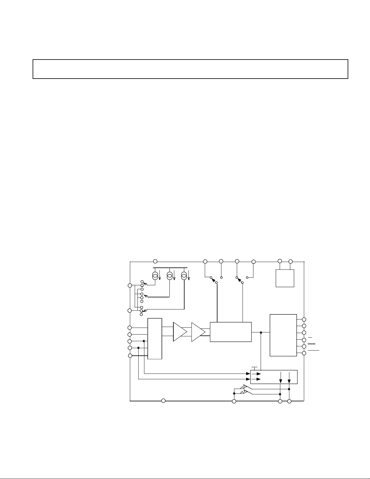
The AD7709 is a complete analog front-end for low
frequency measurement applications. The AD7709
contains a 16-bit sigma delta ADC with PGA and can be
configured as 2 fully-differential input channels or 4
pseudo-differential input channels. Inputs signal ranges
from 20mV to 2.56V can be directly converted using the
AD7709. These signals can be converted directly from a
transducer without the need for signal conditioning. Other
on-chip features include three software configurable
current sources, switchable reference inputs, low side
power switches and a 4-bit digital I/O port.
The device operates from a 32kHz crystal with an onboard PLL generating the required internal operating
frequency. The output data rate from the part is software
programmable. The pk-pk resolution from the part varies
with the programmed gain and output data rate.
The part operates from a single +3V or +5V supply.
When operating from +3V supplies, the power dissipation
for the part is XmW. The AD7709 are housed in a 24pin SOIC and TSSOP packages.
APPLICATIONS
Industrial Process Control
Instrumentation
Pressure Transducers
Portable Instrumentation
IOUT 1
IOUT 2
AIN1
AIN2
AIN3 / P3
AIN4 / P4
AINCOM
VDD
MUX
FUNCTIONAL BLOCK DIAGRAM
REFIN2(+)
I2 I3
I1
BUF
PGA
REFIN1(+)
16-BIT
Σ−∆
REFIN2(-)
ADC
AD7709
GND
PWRGND
REFIN1(-)
VDD
XTAL1 XTAL2
INTERFACE
CONTROL
I/O PORT
OSC
&
PLL
SERIAL
&
LOGIC
.
DOUT
DIN
SCLK
CS
RDY
RESET
SW2/P2SW1/P1
REV. PrA January 2001
Information furnished by Analog Devices is believed to be accurate and
reliable. However, no responsibility is assumed by Analog Devices for its
use, nor for any infringements of patents or other rights of third parties
which may result from its use. No license is granted by implication or
otherwise under any patent or patent rights of Analog Devices.
® SPIand QSPI are a Registered Trademark of Motorola Inc.
® MICROWIRE is a Registered Trademark of National Semiconductor Corp.
One T ec hnology Wa y , P.O. Box 9106, Norwood, MA 02062-9106, U.S.A.
Tel: 781/329-4700 World Wide Web Site: http://www.analog.com
Fax: 781/326-8703
Analog Devices, Inc., 2001
Page 2

PRELIMINARY TECHNICAL DATA
AD7709-SPECIFICATIONS
1
PARAMETER B Grade Units Test Conditions
Output Update Rate 5.4 Hz min.
105 Hz max. 0.021Hz (0.732msec.) increments
No Missing Codes 16 bits min.
Resolution 13 bits pk-pk +20mV range, 20Hz Update Rate
16 bits pk-pk +2.56V range, 20Hz Update Rate
Output Noise and Update Rates See Tables Below in ADC Description
Integral Nonlinearity 15 ppm of FSR max.
Offset Error TBD
Offset Error Drift Vs Temp 10 nV/°C typ.
Offset Error Drift Vs Time TBD nV/1000 Hours typ.
Gain Error TBD
Gain Error Drift Vs Temp 1 ppm/°Ctyp.
Gain Error Drift Vs Time TBD ppm/1000 Hours typ.
Power Supply Rejection(PSR) 90 dB min. Input Range = ±20mV
90 dB min. Input Range = ±2.56V
Common Mode Rejection(CMR)
On AIN 90 dB min. At DC, Range = ±20mV
On AIN 90 dB min. At DC, Range = ±2.56V
On REFIN 90 dB min. At DC, Range = ±20mV
On REFIN 90 dB min. At DC, Range = ±2.56V
Analog Input Current
DC Bias Current 1 nA max.
DC Bias Current Drift TBD nA typ.
DC Offset Current TBD nA typ.
DC Offset Current Drift TBD nA typ.
(VDD = +3V or +5.0V , REFIN(+) = +2.5V; REFIN(-) = 0V;
XTAL1/XTAL2 = 32 kHz Crystal;
All specifications T
MIN
to T
unless otherwise noted.)
MAX
REFERENCE INPUTS (REFIN1& REFIN2)
Normal Mode
50Hz/60Hz Rejection 60 dB min.
Reference DC Input Current T BD µA typ.
REFIN(+) to REFIN(-) Voltage +2.5V nom. REFIN referes to both REFIN1 and REFIN2
REFIN(+) to REFIN(-) Range +1 V min.
V
REFIN Common Mode Range GND-30mV V min.
REFIN Common Mode
50/60Hz Rejection T B D dB min.
ANALOG INPUTS
Normal Mode 50Hz/60Hz Rejection 60 dB min. 50/60Hz ±1Hz , 20Hz Update Rate
Common Mode 50/60Hz Rejection 90 dB min. 50/60Hz ±1Hz, Range = ±20mV
Differential Input Voltage Ranges
Pseudo-Differential Input Voltage Ranges
Full-scale Range Matching 5 uV typ.
Absolute Ain Voltage Limits
Buffered Inputs GND+50mV V min.
Unbuffered Inputs GND-30mV Vmin
DD
V
+30mV V max.
DD
90 dB min. 50/60Hz ±1Hz, Range = ±2.5V
±REFIN/GAIN V nom. REFIN refers to both REFIN1 and
0V to REFIN/GAINV nom.
V
-50mV V max
DD
V
+30mV Vmax
DD
V max.
REFIN2.
REFIN=REFIN(+ )-REFIN(-)
GAIN=1to 128.
–2–
REV. PrA January 2001
Page 3

PRELIMINARY TECHNICAL DATA
PARAMETER B Grade Units Test Conditions
LOGIC INPUTS
All Inputs Except SCLK and XTAL1
V
, Input Low Voltage 0.8 V max. V
INL
V
, Input Low Voltage 0.4 V max. V
INL
V
, Input High Voltage 2.0 V min. V
INH
SCLK Only (Schmitt Triggered Input)
V
T(+)
V
T(-)
V
T(+)- VT(-)
V
T(+)
V
T(-)
V
T(+)-VT(-)
1.4/3 V min/V max VDD = 5V
0.8/1.4 V min/V max VDD = 5V
0.4/0.85 V min/V max VDD = 5V
0.95/2.5 V min/V max VDD = 3V
0.4/1.1 V min/V max VDD = 3V
0.4/0.85 V min/V max VDD = 3V
XTAL1 Only
V
, Input Low Voltage 0.8 V max. V
INL
V
, Input High Voltage 3.5 V min. V
INH
V
, Input Low Voltage 0.4 V max. V
INL
V
, Input High Voltage 2.5 V min. V
INH
Input Currents ±10 µA max. V
Input Capacitance 10 pF typ. All Digital Inputs
LOGIC OUTPUTS (Excluding XTAL2)
V
, Output High Voltage VDD- 0.6 V min. VDD = 3V, I
OH
V
, Output Low Voltage 0.4 V max. VDD = 3V, I
OL
V
, Output High Voltage 4 V min. VDD = 5V, I
OH
V
, Output Low Voltage 0.4 V max. VDD = 5V, I
OL
Floating State Leakage Current ±10 uA max.
Floating State Output Capacitance ±10 pF typ.
Data Output Coding Binary Unipolar Mode
Offset Binary Bipolar Mode
EXCITATION CURRENT SOURCES
I1 and I2 Output Current 200 µA nom.
I3 Output Current 25 µA nom.
Initial Tolerance at 25°C ±10 % typ.
Drift 20 ppm/°C typ.
Initial Current Matching at 25°C ±1 % Matching between I1 and I2
Drift Matching 1 ppm/°C typ.
Line Regulation (V
) TBD nA/V max. VDD = 5V±10%
DD
Load Regulation TBD nA/V max.
Output Compliance AVDD-0.5 V max.
Low-Side Power Switches (SW1 and SW2)
Ron 5 Ω typ VDD = 5V
7 Ω typ V
Allowable Current 20 mA max Per Switch
SYSTEM CALIBRATION
Full-Scale Calibration Limit 1.05 X FS V max.
Zero-Scale Calibration Limit -1.05 X FS V min.
Input Span 0.8 X FS V min.
2.1 X FS V max.
START UP TIME
From Power-On 500 msec typ.
From Idle Mode 1 msec. typ.
From Power-Down Mode 1 msec. typ.
500 msec. typ. Osc. powered down
POWER REQUIREMENTS
Power Supply Voltages
V
- GND 2.7/3.6 V min/max V
DD
4.5/5.5 V min/max V
= 5V
DD
= 3V
DD
= 3V or 5V
DD
= 5V
DD
= 5V
DD
= 3V
DD
= 3V
DD
= 0V or V
IN
= 3V
DD
= 3V nom.
DD
= 5V nom.
DD
DD
SOURCE
= 100µA
SINK
SOURCE
= 1.6mA
SINK
= 100µA
= 200µA
AD7709
REV. PrA January 2001
–3–
Page 4

PRELIMINARY TECHNICAL DATA
AD7709
PARAMETER B Grade Units Test Conditions
Power Supply Currents
VDD Current (Normal Mode) TBD mA VDD=3V
V
Current (Normal Mode) TBD mA VDD=5V
DD
Current (Idle Mode) TBD mA VDD=3V
V
DD
V
Current (Idle Mode) TBD mA VDD=5V
DD
Current (Power-Down Mode) 20 µA max. VDD=3V, 32.768kHz Osc. Running
V
DD
VDD Current (Power-Down Mode) 30 µA max. VDD=5V, 32.768kHz Osc. Running
NOTES
1
Temperature Range -40
2
3
4
°C
to +85
°C
–4–
REV. PrA January 2001
Page 5
PRELIMINARY TECHNICAL DATA
ABSOLUTE MAXIMUM RATINGS
(TA = +25°C unless otherwise noted)
V
to GND.............................................-0.3V to +7V
DD
Analog Input Voltage to GND...........-0.3V to V
Reference Input Voltage to GND.......-0.3V to V
AIN/REFIN Current (Indefinite)...........................30mA
Digital Input Voltage to GND...........-0.3V to V
Digital Output Voltage to GND........-0.3V to V
PWRGND
to GND...............................-0.3V to +0.3V
Operating Temperature Range..................-40°C to 85°C
Storage Temperature Range....................-65°C to 150°C
Junction Temperature........................................+150°C
PACKAGE Power Dissipation........................TBD mW
θ
Thermal Impedance..................................90°C/W
JA
Lead Temperature, Soldering
Vapor Phase (60sec)..................................+215°C
Infrared (15 sec).......................................+220°C
1
Stresses above those listed under "Absolute Maximum Ratings" may cause permanent
damage to the device. This is a stress rating only and functional operation of the device
at these or any other conditions above those listed in the operational sections of this
specification is not implied. Exposure to absolute maximum rating conditions for
extended periods may affect device reliability.
1
+0.3V
DD
+0.3V
DD
+0.3V
DD
+0.3V
DD
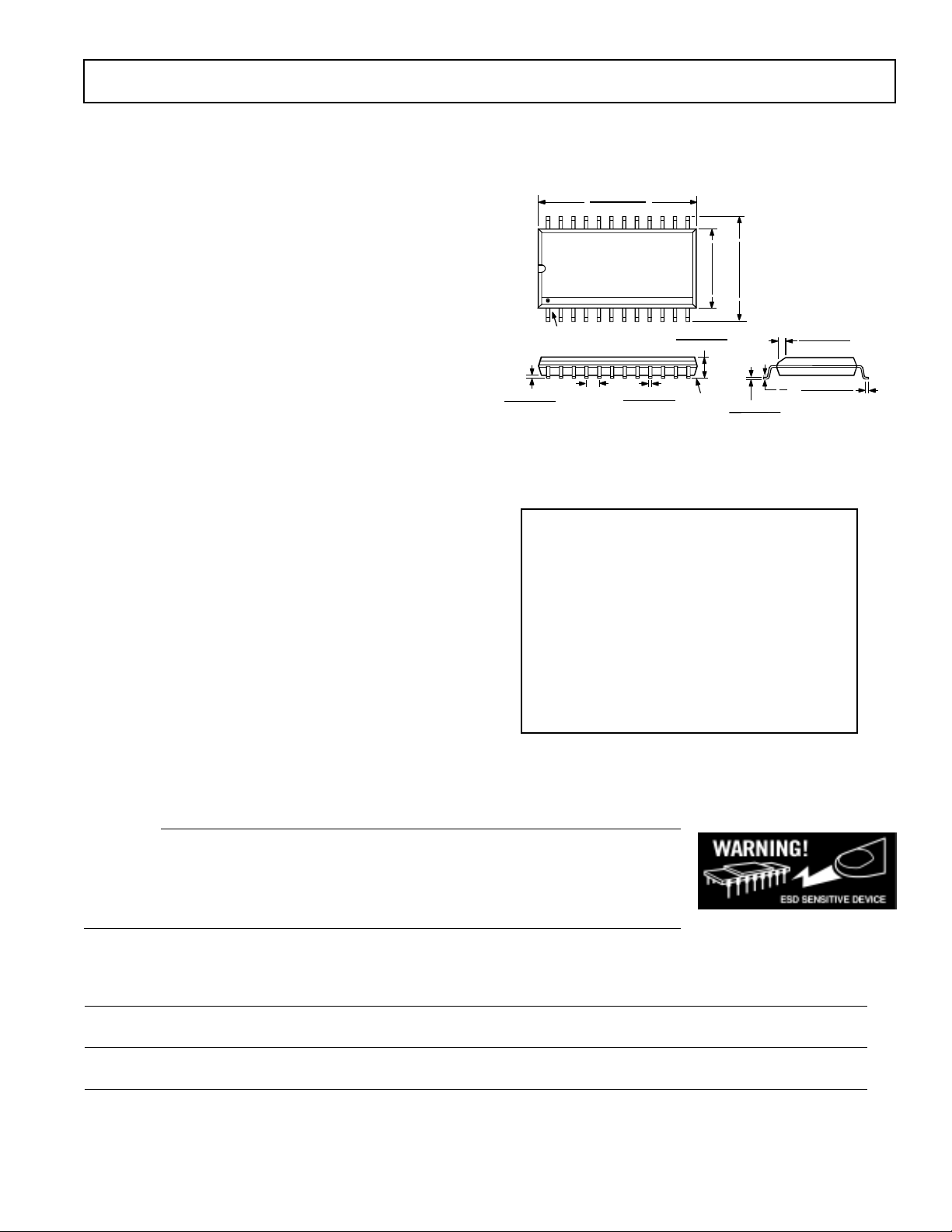
OUTLINE DIMENSIONS
24-lead plastic SOIC (R-24)
0.6141 (15.60)
0.5985 (15.20)
24
1
0.0118 (0.30)
0.0040 (0.10)
PIN 1
0.0500
(1.27)
BSC
0.0192 (0.49)
0.0138 (0.35)
13
12
0.1043 (2.65)
0.0926 (2.35)
SEATING
PLANE
24-lead plastic TSSOP (RU-24)
7.40)
7.60)
0.2914 (
0.2992 (
0.0125 (0.32)
0.0091 (0.23)
AD7709
10.00)
10.65)
0.3937 (
0.4193 (
0.0291 (0.74)
0.0098 (0.25)
0.0500 (1.27)
8¡
0¡
0.0157 (0.40)
x 45¡
24-lead plastic
TSSOP (RU-24)
CAUTION
ESD (electrostatic discharge) sensitive device. Electrostatic charges as high as 4000 V readily
accumulate on the human body and test equipment and can discharge without detection.
Although the AD7709 features proprietary ESD protection circuitry, permanent damage may
occur on devices subjected to high energy electrostatic discharges. Therefore, proper ESD
precautions are recommended to avoid performance degradation or loss of functionality.
ORDERING GUIDE
Model Temperature Package Package Drawing
Range Description Option
AD7709BR -40°C to +85°C SOIC R-24
AD7709BRU -40°C to +85°C TSSOP RU-24
–5–REV. PrA January 2001
Page 6

AD7709
PRELIMINARY TECHNICAL DATA
TIMING CHARACTERISTICS
1, 2
(VDD = +3V ±10% or VDD = +5V ±10%;GND = 0 V:X
= 32.768kHz; Input Logic 0 = 0 V, Logic 1 = V
TAL
DD
unless otherwise noted)
Limit at T
MIN
, T
MAX
Parameter (B Version) Units Conditions/Comments
t
1
t
2
32.768 kHz typ Crystal Oscillator Frequency.
50 ns min RESET Pulse Width
Read Operation
t
3
t
4
4
t
5
0 ns min RDY to CS Setup Time
0 ns min CS Falling Edge to SCLK Active Edge Setup
0 ns min SCLK Active Edge to Data Valid Delay
Time
3
3
60 ns max VDD = +4.5 V to +5.5 V
4, 5
t
5A
80 ns max V
0 ns min CS Falling Edge to Data Valid Delay
= +2.7 V to +3.6 V
DD
3
60 ns max VDD = +4.5 V to +5.5 V
80 ns max V
t
6
t
7
t
8
6
t
9
100 ns min SCLK High Pulse Width
100 ns min SCLK Low Pulse Width
0 ns min CS Rising Edge to SCLK Inactive Edge Hold
10 ns min Bus Relinquish Time after SCLK Inactive Edge
80 ns max
t
10
100 ns max SCLK Active Edge to RDY High
= +2.7 V to +3.6 V
DD
3
Time
3
3, 7
Write Operation
t
11
t
12
t
13
t
14
t
15
t
16
NOTES
1
Sample tested during initial release to ensure compliance. All input signals are specified with tr = tf = 5 ns (10% to 90% of VDD) and timed from a voltage level of 1.6 V.
2
See Figures 1 and 2.
3
SCLK active edge is falling edge of SCLK.
4
These numbers are measured with the load circuit of Figure 3 and defined as the time required for the output to cross the VOL or VOH limits.
5
This specification only comes into play if CS goes low while SCLK is low. It is required primarily for interfacing to DSP machines.
6
These numbers are derived from the measured time taken by the data output to change 0.5 V when loaded with the circuit of Figure 3. The measured number is then extrapolated back to remove effects of charging or
discharging the 50 pF capacitor. This means that the times quoted in the timing characteristics are the true bus relinquish times of the part and as such are independent of external bus loading capacitances.
7
RDY returns high after the first read from the device after an output update. The same data can be read again, if required, while RDY is high, although care should be taken that subsequent reads do not occur close to
the next output update.
0 ns min CS Falling Edge to SCLK Active Edge Setup
Time
3
30 ns min Data Valid to SCLK Edge Setup Time
25 ns min Data Valid to SCLK Edge Hold Time
100 ns min SCLK High Pulse Width
100 ns min SCLK Low Pulse Width
0 ns min CS Rising Edge to SCLK Edge Hold Time
–6–
REV. PrA January 2001
Page 7

CS
PRELIMINARY TECHNICAL DATA
AD7709
SCLK
DIN
RDY
CS
SCLK
t
11
t
12
MSB
t
13
t
14
t
15
LSB
t
16
Figure 1. Write Cycle Timing Diagram
t
3
t
4
t
6
t
10
t
8
DOUT
t
t
5
t
5A
MSB
7
t
6
t
9
LSB
Figure 2. Read Cycle Timing Diagram
–7–REV. PrA January 2001
Page 8

AD7709
PRELIMINARY TECHNICAL DATA
PIN CONFIGURATION
IOUT 1
IOUT 2
REFIN1(+)
REFIN1(-)
AIN1
AIN 2
AIN3/P3
AIN4/P4
AINCOM
REFIN2(+)
REFIN2(-)
P2/SW2
1
2
3
AD7709
4
5
TOP VIEW
(Not to Scale)
6
7
8
9
10
11
12
24
23
22
21
20
19
18
17
16
15
14
13
XTAL1
XTAL2
V
DD
GND
DIN
DOUT
DRDY
CS
SCLK
RESET
P1/SW1
PWRGND
Pin Function Description
Pin No Mnemonic Function
1 IOUT1 Output for internal excitation current sources. A single current source or any
combination of the internal current sources I1,I2 and I3 can be switched to this
output.
2 IOUT2 Output for internal excitation current sources. A single current source or any
combination of the internal current sources I1,I2 and I3 can be switched to this
output.
3 REFIN1(+) Positive reference input. REFIN(+) can lie anywhere between V
The nominal reference voltage (REFIN(+)-REFIN(-)) is 2.5V but the part is
functional with a reference range from 1V to V
DD
.
4 REFIN1(-) Negative reference input. This reference input can lie anywhere between GND
and V
DD
-1V.
5 AIN1 Analog Input Channel 1. Programmable-gain analog input which can be used
as a pseudo-differential input when used with AINCOM or as the positive input of a fully-differential input pair when used with AIN2. (see Communications Register section)
6 AIN2 Analog Input Channel 2. Programmable-gain analog input which can be used
as a pseudo-differential input when used with AINCOM or as the negative
input of a fully-differential input pair when used with AIN1. (see Communications Register section)
7 AIN3/P3 Analog Input Channel 3 or Digital Port Bit. Programmable-gain analog input
which can be used as a pseudo-differential input when used with AINCOM or
as the positive input of a fully-differential input pair when used with AIN4.
The second function of this bit is as a general purpose digital input bit.
8 AIN4/P4 Analog Input Channel 4 or digital port bit. Programmable-gain analog input
which can be used as a pseudo-differential input when used with AINCOM or
as the negative input of a fully-differential input pair when used with AIN3.
The second function of this bit is as a general purpose digital input bit.
9 AINCOM All analog inputs are referenced to this input when configured in pseudo-dif-
ferential input mode.
10 REFIN2(+) Positive reference input. REFIN2(+) can lie anywhere between V
The nominal reference voltage (REFIN2(+)-REFIN2(-)) is 2.5V but the part
is functional with a reference range from 1V to V
DD
.
and GND.
DD
and GND.
DD
–8–
REV. PrA January 2001
Page 9

PRELIMINARY TECHNICAL DATA
AD7709
11 REFIN2(-) Negative reference input. This reference input can lie anywhere between GND
and V
12 P2/SW2 P2 can act as a general purpose Input/Output bit referenced between V
GND or as a low-side power switch to PWRGND..
13 PWRGND Ground point for the low-side power switches SW2 and SW1. PWRGND
must be tied to GND.
14 P1/SW1 P1 can act as a general purpose Output bit referenced between V
or as a low-side power switch to PWRGND.
15 RESET Digital input used to reset the ADC to its power-on-reset status. This pin has
a weak pull-up internally to DV
16 SCLK Serial clock input for data transfers to and from the ADC. The SCLK has a
schmitt triggered input making the interface suitable for opto-isolated applications. The serial clock can be continuous with all data transmitted in a continuous train of pulses. Alternatively, it can be noncontinuous clock with the
information being transmitted to or from the AD7709 in smaller batches of
data.
17 CS Chip Select Input. This is an active low logic input used to select the
AD7709. CS can be used to select the AD7709 in systems with more than one
device on the serial bus or as a frame synchronisation signal in communicating
with the device. CS can be hardwired low allowing the AD7709 to be operated
in three-wire mode with SCLK, DIN and DOUT used to interface with the
device.
18 RDY RDY is a logic low status output from the AD7709. RDY is low if the ADC
has valid data in its data register. This output returns high on completion of a
read operation from the data register. If data is not read, RDY will return high
prior to the next update indicating to the user that a read operation should not
be initiated.
19 DOUT Serial data output with serial data being read from the output shift register of
the ADC. The output shift register can contain data from any of the on-chip
data, calibration or control registers.
20 DIN Serial Data Input with serial data being written to the input shift register on
the AD7709. Data in this shift register is transferred to the control registers
within the ADC depending on the selection bits of the Communications regis-
ter.
21 GND Ground Reference point for the AD7709.
22 V
23 XTAL2 Output from the 32kHz crystal oscillator inverter.
24 XTAL1 Input to the 32kHz crystal oscillator inverter.
DD
Supply voltage, 3V or 5V nominal.
DD
-1V.
DD
and
DD
and GND
DD
.
–9–REV. PrA January 2001
Page 10

PRELIMINARY TECHNICAL DATA
AD7709
ADC CIRCUIT INFORMATION
Overview
The AD7709 incorporates an analog multiplexer with a Sigma-Delta ADC, on-chip programmable gain amplifier and
digital filtering intended for the measurement of wide dynamic range, low frequency signals such as those in weigh-scale,
strain-gauge, pressure transducer or temperature measurement applications. The AD7709 offers 16-bit resolution. The
AD7709 can be configured as 2 fully differential input channels or as 4 pseudo differential input channels referenced to
AINCOM. The channel is buffered and can be programmed for one of 8 input ranges from
the input channel means that the part can handle significant source impedances on the analog input and that R, C
filtering (for noise rejection or RFI reduction) can be placed on the analog inputs if required. These input channels are
intended to convert signals directly from sensors without the need for external signal conditioning. Other functions
contained on-chip that augment the operation of the ADC include software configurable current sources, switchable
reference inputs and low side power switches.
The ADC employs a sigma-delta conversion technique to realize up to 16-bits of no missing codes performance. The
sigma-delta modulator converts the sampled input signal into a digital pulse train whose duty cycle contains the digital
information. A Sinc
3
programmable low pass filter is then employed to decimate the modulator output data stream to
give a valid data conversion result at programmable output rates from 5.35Hz (186.77mS) to 105.03Hz (9.52mS). A
Chopping scheme is also employed to minimize ADC channel offset errors. A block diagram of the ADC input channel
is shown in Figure 3 below.
+20mV to +2.56V. Buffering
Analog
Input
f
chop
Mux MOD0
Buffer PG A
f
in
f
S-D
mod
Figure 3. AD7709 ADC Channel Block Diagram
ff
chop adc
XOR
3
1
×
SF
8
∑
Sinc3 Filter
()
1
∑
×
(83
SF)
×
--2
Ain+ V
A
- V
in
os
os
Digital
Output
–10–
REV. PrA January 2001
Page 11

PRELIMINARY TECHNICAL DATA
AD7709
ADC NOISE PERFORMANCE
Tables I and II below show the output rms noise and output peak-to-peak resolution in bits (rounded to the nearest
0.5LSB) for some typical output update rates . The numbers are typical and generated at a differential input voltage of
0V. The output update rate is selected via the SF7-SF0 bits in the Filter Register. It is important to note that the peakto-peak resolution figures represent the resolution for which there will be no code flicker within a six-sigma limit.
output noise comes from two sources. The first is the electrical noise in the semiconductor devices (device noise) used in
the implementation of the modulator. Secondly, when the analog input is converted into the digital domain, quantization
noise is added. The device noise is at a low level and is independant of frequency. The quantization noise starts at an even
lower level but rises rapidly with increasing frequency to become the dominant noise source.The numbers in the tables are
given for the bipolar input ranges. For the unipolar ranges the rms noise numbers will be the same as the bipolar range
but the peak to peak resolution is now based on half the signal range which effectively means loosing 1 bit of resolution.
Table I. Typical Output RMS Noise vs. Input Range and Update Rate for AD7709
Output RMS Noise in µV
SF Data Update Input Range
Word Rate (Hz) ±20mV ±40mV ±80mV ±160mV ±320mV ±640mV ±1.24V ±2.56V
13 105.3 1.50 1.50 1.60 1.75 3.50 4.50 6.70 11.75
69 19.79 0.60 0.65 0.65 0.65 0.65 0.95 1.40 2.30
255 5.35 0.35 0.35 0.37 0.37 0.37 0.51 0.82 1.25
The
Table II. Peak-to-Peak Resolution vs. Input Range and Update Rate for AD7709
Peak-to-Peak Resolution in Bits
SF Data Update Input Range
Word Rate (Hz) ±20mV ±40mV ±80mV ±160mV ±320mV ±640mV ±1.24V ±2.56V
13 105.3 12 13 14 15 15 15.5 1 6 16
69 19.79 13 14 15 16 16 16 1 6 16
255 5.35 14 1 5 16 16 16 16 16 16
AD7709 ON-CHIP REGISTERS
Both the AD7709 is controlled and configured via 4 on-chip registers as shown in figure 4 and described in more detail
in the following section. In the following descriptions, SET implies a logic 1 state and CLEARED implies a logic 0 state
unless otherwise stated.
DIN
DOUT
DIN
DOUT
DOUT
Comm unications Register
OSCPD
STBY
R/WWEN
Statu s Register
DIN
Configuration Register(24-Bits)
0
0A1
A0
REGISTER
SELECT
DECODER
DOUT
DOUT
DIN
Filter Register
ADC Data Register
Figure 4. AD7709 On-Chip Registers
–11–REV. PrA January 2001
Page 12

PRELIMINARY TECHNICAL DATA
AD7709
Communications Register- ( A1, A0= 0,0):
The Communications Register is an 8-bit write-only register. All communications to the part must start with a write
operation to the Communications Register. The data written to the Communications Register determines whether the
next operation is a read or write operation, the type of read operation and to which register this operation takes place.
For read or write operations, once the subsequent read or write operation to the selected register is complete, the interface returns to where it expects a write operation to the Communications Register. This is the default state of the interface, and on power-up or after a RESET, the AD7709 is in this default state waiting for a write operation to the
Communications Register. In situations where the interface sequence is lost, a write operation of at least 32 serial clock
cycles with DIN high, returns the AD7709 to this default state by resetting the part. Table III outlines the bit designations for the Communications Register. CR0 through CR7 indicate the bit location, CR denoting the bits are in the
Communications Register. CR7 denotes the first bit of the data stream.
CR7 CR6 CR5 CR4 CR3 CR2 CR1 CR0
WEN(0) R/W(0) STBY(0) OSCPD (0) 0 (0) 0(0) A1(0) A(0)
Table III. Communications Register Bit Designations
Bit Bit
Location Mnemonic Description
CR7 WEN Write Enable Bit. A 0 must be written to this bit so the write operation to the Communications
Register actually takes place. If a 1 is written to this bit, the part will not clock on to subsequent bits in the register. It will stay at this bit location until a 0 is written to this bit. Once a 0
is written to the WEN bit, the next seven bits will be loaded to the Communications Register.
CR6 R/W A zero in this bit location indicates that the next operation will be a write to a specified regis-
ter. A one in this position indicates that the next operation will be a read from the designated
register.
CR5 STBY Standby bit indication.
Set when its required to put the AD7709 in low power mode.
Clear to power up the AD7709.
CR4 OSCPD Oscillator Power Down Bit.
If this bit is set, then placing the AD7709 in standby mode will stop the crystal oscillator reducing the power drawn by these parts to a minimum. The oscillator will require 500ms to begin
oscillating when the ADC is taken out of standby mode.
If this bit is cleared the oscillator is not shut off when the ADC is put into standby mode and
will not require the 500ms start-up time when the ADC is taken out of standby.
CR3 0 This bit must be programmed with a logic 0 for correct operation.
CR2 0 This bit must be programmed with a logic 0 for correct operation.
CR1-CR0 A1-A0 Register Address Bits. These address bits are used to address the AD7709’s registers and are
outlined in table IV.
Table IV. AD7709 Register Selection Table
A1 A0 Register
0 0 Communications register during a write operation.
0 0 Status Register register during a read operation.
0 1 Configuration Register
1 0 Filter register
1 1 ADC Data Register
–12–
REV. PrA January 2001
Page 13

PRELIMINARY TECHNICAL DATA
AD7709
Status Register - (A1,A0=0,0; Power-On-Reset = 00Hex):
The ADC Status Register is an 8-bit read-only register. To access the ADC Status Register, the user must write to the
Communications Register selecting the next operation to be a read and load bits A1-A0 with 0,0. Table V outlines the
bit designations for the Status Register. SR0 through SR7 indicate the bit location, SR denoting the bits are in
the Status Register. SR7 denotes the first bit of the data stream. The number in brackets indicates the power-on/reset
default status of that bit.
SR7 SR6 SR5 SR4 SR3 SR2 SR1 SR0
RDY(0) 0(0) 0(0) 0(0) ERR (0) 0(0) STBY(0) LOCK(0)
Table V. Status Register Bit Designations
Bit Bit
Location Mnemonic Description
SR7 RDY Ready bit for the ADC
Set when data is transferred to the ADC data register.
The RDY bit is cleared automatically a period of time before the data register is updated with a
new conversion result or after the ADC data register has been read.
SR6 0 Bit is automatically cleared. Reserved for future use
SR5 0 This bit is automatically cleared. Reserved for future use
SR4 0 This bit is automatically cleared. Reserved for future use
SR3 ERR ADC Error Bit. This qualifying bit is set at the same at the RDY bit.
When Set it indicates that the result written to the ADC data register has been clamped to all
zeros or all ones. Error sources include Overrange and loss of lock.
This bit is Cleared at the same time as the RDY bit.
SR2 0 This bit is automatically cleared. Reserved for future use
SR1 STBY Standby bit indication.
When Set it indicates that the AD7709 is in low power mode.
Cleared when the ADC is powerd up.
SR0 LOCK PLL lock status bit.
This bit is SET if the PLL has locked onto the 32kHz crystal oscillator clock. The ADC will
not start conversion till this bit has been set. If the LOCK bit subsequently goes low the ERR
bit will be set.
Configuration Register(CONFIG) :(A1,A0 = 0,1; Power-On-Reset = 000000Hex)
The CONFIG Register is a 24-bit register from which data can either be read or to which data can be written. This
register is used to select the input channel and configure the input range, excitation current sources and I/O port.Table
XIII outlines the bit designations for this register. CONFIG24 through CONFIG0 indicate the bit location, CONFIG
denoting the bits are in the Configuration Register. CONFIG24 denotes the first bit of the data stream. The number in
brackets indicates the power-on/reset default status of that bit. A write to the CONFIG register has immediate effect and
does not reset the the ADCs. Thus , if a current source is switched while the ADC is converting the user will have to wait
for the fullsettling time of the sinc^3 filter before getting a fully settled output. This equates to 4 outputs.
–13–REV. PrA January 2001
Page 14

PRELIMINARY TECHNICAL DATA
AD7709
CONFIG23 CONFIG22 CONFIG21 CONFIG20 CONFIG19 CONFIG18 CONFIG17 CONFIG16
PSW1(0) PSW2(0) I3EN1 (0) I3EN1(0) I2EN1(0) I2EN0(0) I1EN1(0) I1EN0(0)
CONFIG15 CONFIG14 CONFIG13 CONFIG12 CONFIG11 CONFIG10 CONFIG9 CONFIG8
P4DIG(0) P3DIG(0) P2EN(0) P1EN(0) P4DAT(0) P3DAT(0) P2DAT(0) P1DAT(0)
CONFIG7 CONFIG6 CONFIG5 CONFIG4 CONFIG3 CONFIG2 CONFIG1 CONFIG0
REFSEL(0) CH2(0) CH1(0) CH0(0) UNI(0) RN2(0) RN1(0) RN0(0)
Table VI. Configuration Register Bit Designations
Bit Bit
Location Mnemonic Description
CONFIG23 PSW1 Power Switch 1 Control bit.
Set by user to enable Power switch P1 to PWRGND.
Cleared by user to enable use as a standard I/O pin.
When ADC is in standby mode the power switches are open.
CONFIG22 PSW2 Power Switch 2 Control bit.
Set by user to enable Power switch P2 to PWRGND.
Cleared by user to enable use as a standard I/O pin.
When ADC is in standby mode the power switches are open.
CONFIG21 I3EN1 Current Source Enable Bits. Used in conjunction with bit I3EN0 to determine the function
of current source I3
CONFIG20 I3EN0 Current Source Enable Bits. Used in conjunction with bit I3EN1 to determine the function
of current source I3
I3EN1 I3EN0 Function
0 0 Current Source OFF
0 1 Current Source Routed to IOUT1 pin.
1 0 Current Source Routed to IOUT2 pin.
1 1 Current Source Routed to GND
CONFIG19 I2EN1 Current Source Enable Bits. Used in conjunction with bit I2EN0 to determine the function
of current source I2
CONFIG18 I2EN0 Current Source Enable Bits. Used in conjunction with bit I2EN1 to determine the function
of current source I2
I2EN1 I2EN0 Function
0 0 Current Source OFF
0 1 Current Source Routed to IOUT1 pin.
1 0 Current Source Routed to IOUT2 pin.
1 1 Current Source Routed to GND
CONFIG17 I1EN1 Current Source Enable Bits. Used in conjunction with bit I1EN0 to determine the function
of current source I3
CONFIG16 I1EN0 Current Source Enable Bits. Used in conjunction with bit I1EN1 to determine the function
of current source I3
I1EN1 I1EN0 Function
0 0 Current Source OFF
0 1 Current Source Routed to IOUT1 pin.
1 0 Current Source Routed to IOUT2 pin.
1 1 Current Source Routed to GND
CONFIG15 P4DIG Digital Input Enable
Set by user to enable P4 as a digital input
Cleared by user to configure as pin P4/AIN4 as analog input.
–14–
REV. PrA January 2001
Page 15

PRELIMINARY TECHNICAL DATA
AD7709
CONFIG14 P3DIG Digital Input Enable
Set by user to enable P3 as a digital input
Cleared by user to configure as pin P3/AIN3 as analog input. The default configuration is
analog input.
CONFIG13 P2EN P2 digital output enable bit.
Set by user to enable P2 as a regular digital output pin.
Cleared by user to tristate P2 output.
PSW2 takes presedance over P2EN.
CONFIG12 P1EN P1 digital output enable bit.
Set by user to enable P1 as a regular digital output pin.
Cleared by user to tristate P1 output.
PSW1 takes presedance over P1EN.
CONFIG11 P4DAT Digital input port data bit. P4DAT is read only and will return a 0 if P4DIG=0. If P4 is
enabled as a digital input then the read back value indicates the status of pin P4.
CONFIG10 P3DAT Digital input port data bit. P3DAT is read only and will return a 0 if P3DIG=0. If P3 is
enabled as a digital input then the read back value indicates the status of pin P3.
CONFIG9 P2DAT Digital output port data bit. P2 is digital output only. When the port is active as an output
(P2EN=1), then the value written to the this data bit appears at the output port. Reading
P2DAT will return what was last written to the P2DAT bit on the AD7709.
CONFIG8 P1DAT Digital output port data bit. P1 is digital output only. When the port is active as an output
(P1EN=1), then the value written to the this data bit appears at the output port. Reading
P1DAT will return what was last written to the P1DAT bit on the AD7709.
CONFIG7 REFSEL ADC reference input select.
Cleared by user to select REFIN1(+) and REFIN1(-) as the ADC reference.
Set by user to select REFIN2(+) and REFIN2(-) as the ADC reference.
CONFIG6 CH2 ADC Input Channel Selection bit. Used in conjunction with CH1 and CH0 as shown in
the analog input selection table.
CONFIG5 CH1 ADC Input Channel Selection bit. Used in conjunction with CH2 and CH0 as shown in
the analog input selection table.
CONFIG4 CH0 ADC Input Channel Selection bit. Used in conjunction with CH2 and CH2 as shown in
the analog input selection table.
CH2 CH1 CH0 Positive Input Negative Input Buffer
0 0 0 AIN1 AINCOM Positive Analog Input
0 0 1 AIN2 AINCOM Positive Analog Input
0 1 0 AIN3 AINCOM Positive Analog Input
0 1 1 AIN4 AINCOM Positive Analog Input
1 0 0 AIN1 AIN2 Positive and Negative Analog Inputs
1 0 1 AIN3 AIN4 Positive and Negative Analog Inputs
1 1 0 AINCOM AINCOM Positive and Negative Analog Inputs
The final column indicates if the analog inputs are buffered or unbuffered. This determines the common mode
input range on each input. If the input is unbuffered (AINCOM) the common mode input includes GND.
CONFIG3 UNI Unipolar/Bipolar Operation Selection Bit.
Set by user to enable unipolar operation with straight binary output coding i.e. zero differential input will result in 0000hex output and a fullscale differential input will result in
FFFF Hex output.
Cleared by user to enable pseudo bipolar operation and offset binary coding, negative
fullscale differential input will result in an output code of 0000 Hex, zero differential input will result in an output code of 8000Hex and a positive fullscale differential input will
result in an output code of FFFF Hex.
–15–REV. PrA January 2001
Page 16

PRELIMINARY TECHNICAL DATA
AD7709
CONFIG2 RN2 Used in conjunction with RN1 and RN0 to select the analog input range.
CONFIG1 RN1 Used in conjunction with RN2 and RN0 to select the analog input range.
CONFIG0 RN0 Used in conjunction with RN2 and RN1 to select the analog input range.
RN2 RN1 RN0 Selected Main ADC Input Range (Vref=2.5V)
0 0 0 ±20mV
0 0 1 ±40mV
0 1 0 ±80mV
0 1 1 ±160mV
1 0 0 ±320mV
1 0 1 ±640mV
1 1 0 ±1.28V
1 1 1 ±2.56V
Filter Register:(A1,A0=1,0; Power-On-Reset = 00Hex)
The Filter Register is an 8-bit register from which data can either be read or to which data can be written. This register
determines the amount of averaging performed by the sinc filter. Table VII outlines the bit designations for the Filter
Register. FR7 through FR0 indicate the bit location, FR denoting the bits are in the Filter Register. FR7 denotes the
first bit of the data stream. The number in brackets indicates the power-on/reset default status of that bit. The number in
this register is used to set the decimation factor and thus the output update rate for the ADCs. The filter register cannot
be written to by the user while the ADC is active. The update rate is used for the ADC is calculated as follows :
f
= 1 X 1 X
adc
f
mod
3 8.SF
Where : fadc = ADC Output Update Rate
fmod = Modulator Clock Frequency= 32.768KHz (Main and Aux ADC)
SF = Decimal Value written to SF Register
FR7 FR6 FR5 FR4 FR3 FR2 FR1 FR0
SF7(0) SF6(1) SF5(0) SF4(0) SF3(0) SF2(1) SF1(0) SF0(1)
Table VII. Filter Register Bit Designations
adc
.
) and time
adc
The allowable range for SF is 13dec to 255dec. Examples of SF values and corresponding conversion rate (f
(t
) are shown in table XII below. It should also be noted that both ADC input channels are chopped to minimise offset
adc
errors. This means that the time for a single conversion or the time to the first conversion result is 2 X t
SF(dec) SF(hex) f
13 0D 105.3 9.52
69 45 19.79 50.34
255 FF 5.35 186.77
(Hz) t
adc
adc
(ms)
Table XII. Update Rate Vs SF Word.
ADC Data Result Register (DATA):(A1,A0=1,1; Power-On-Reset = 000000Hex)
The conversion result for the selected ADC channel is stored in the ADC data register (DATA). This register is 16-bits
wide. This is a read only register. On completion of a read from this register the RDY bit in the status register is cleared.
–16–
REV. PrA January 2001
Page 17

PRELIMINARY TECHNICAL DATA
AD7709
CONFIGURING THE AD7709
On the AD7709 there are only four user accessable registers and these are configured via the serial interface. Communication with any of these registers is initiated by firstly writing to the Communications Register. The AD7709 starts converting after a power up without the requiring any register to be written to. The defaults conditions are used and the AD7709
operates at a 20Hz update rate offering 50 and 60Hz rejection.
Figure 5 outlines a flow diagram of the sequence used to configure the registers on the AD7709 following a power-up.
The flowchart shows two methods of determining when its valid to read the data register. The first method is hardware
polling of the RDY pin and the second method involves software interrogation of bits in the status and mode registers. The
flowchart details all the necessary programming steps required to initialize the ADC and read data from the selected ADC channel following a power-on or reset.The steps can be broken down as follows:
1. Configure and initialize the microcontroller or microprocessor serial port.
2. Initialize the AD7709 by configuring the following registers:
a)FILTER registers which determines the update rate. The AD7709 must be put into standby mode before writing to the
filter register.
b) CONFIGURATION register to select the input channel to be converted, its input range and reference. This register is
also used to configure the internal current sources, power switches and I/O port.
Both of these operations consist of a write to the communications register to specify the next operation as a write to a specified
register. Data is then written to this register. When each sequence is complete the ADC defaults to waiting for another write to
the communications register to specify the next operation.
3) When configuration is complete the user needs to determine when its valid to read the data from the data register. This
is accomplished by either polling the RDY pin (hardware polling) or by interrogating the bits in the STATUS register
(software polling). Both are shown in the following flowchart.
START
POWER-ON/RESET FO R AD770 9
CONF I GURE & INITIALIZ E
WRITE TO COMMUNICATIONS REGISTER SELECTING
NEXT OPERATION TO BE A WRITE TO
THE FILTER REGISTER (WRITE 22HEX TO COMMS REG)
WRITE TO FILTER REGISTER TO CONFIGURE
THE REQUIRED UPDATE RATE.
WRITE TO COMMUNICATIONS REGISTER SETTING UP
NEXT OPERATION TO BE A WRITE TO THE
CONFIGURATION REGISTER (WRITE 01Hex TO COMMS REG)
WRITE TO CONFIGURATION REGIST ER TO SE LECT IN PUT
CHANNEL, INPUT RANGE AND REFERENCE. CURRENT
SOURCES AND I/O PORT CAN ALSO BE CONFIGURED
READ DATA FROM OUTPUT REGISTER
HARDWARE
POLLING
mC/m
P SERIAL PORT
SOFTWARE
POLLING
HARDWARE POLLING
RDY
POLL
PIN
NO
RDY
LOW?
WRITE TO COMMUNICATIONS REGISTER SETTING UP
NEXT OPERATION TO BE A READ OF THE
DATA REGISTER (WRITE 43HEX TO COMMS REGISTER)
READ16-BIT DATA RESULT
YES
NO
YES
ANOTHER
READ?
NO
CHANNEL
CHANGE
SOFTWARE POLLING
WRITE TO COMMUNICATIONS REGISTER SETTING UP NEXT
OPERATION TO BE A READ FROM THE STATUS REGISTER
WRITE 40HEX TO COMMS REGISTER
READ STATUS REGISTER
NO
RDY=1
YES
WRITE TO COMMUNICATIONS RE GISTER SETTING UP
NEXT OPERATION TO BE A READ OF THE DATA
REGISTER. WRITE 43HEX TO COMMS REGISTER
READ16-BIT DATA RESULT
YES
YES
ANOTHER
READ?
NO
CHANNEL
CHANGE
END
Figure 5. Flowchart for Configuring and reading from AD7709
–17–REV. PrA January 2001
NO
END
 Loading...