

Page 1
PRELIMINAR Y TECHNICAL D A T A
a
Preliminary Technical Data
FEATURES
18 Bits Resolution with No Missing Codes
No Pipeline Delay ( SAR architecture )
Differential Input Range: 5V
Throughput: 100 kSPS
INL: 2.5 LSB Max (9.5 ppm of Full-Scale)
Dynamic Range : 102 dB Typ
S/(N+D): 100 dB Typ @ 10 kHz
THD: –115 dB Typ @ 10 kHz
Parallel (18, 16 or 8 bits bus) and Serial 5 V/3 V Interface
On-board Reference Buffer
Single 5 V Supply Operation
Power Dissipation: 15 mW @ 100 kSPS
20 mW Typ with internal buffer
Power-Down Mode: 7
Package: 48-Lead Quad Flat Pack (LQFP)
48-Lead Frame Chip Scale Package (LFCSP)
Pin-to-Pin Compatible with the AD7675/AD7679/AD7674
APPLICATIONS
CT Scanners
High Dynamic Data Acquisition
Geophone and hydrophone sensor
Instrumentation
Spectrum Analysis
Medical Instruments
W Max
AGND
AVDD
REFBUFIN
IN+
RESET
18-Bit, 100 kSPS SAR ADC
FUNCTIONAL BLOCK DIAGRAM
REF
REFGND
AD7678
SWITCHED
CAP DAC
CLOCK
CONTROL LOGIC AND
CNVST
SERIAL
PARALLEL
INTERFACE
IN-
PD
PDBUF
CALIBRATION CIRCUITRY
AD7678
DGNDDVDD
PORT
18
OVDD
OGND
DATA[17:0]
BUSY
RD
CS
MODE0
MODE1
GENERAL DESCRIPTION
The AD7678 is a 18-bit, 100 kSPS, charge redistribution
SAR, fully differential analog-to-digital converter that
operates from a single 5 V power supply. The part contains a high-speed 18-bit sampling ADC, an internal
conversion clock, an internal reference buffer, error correction circuits, and both serial and parallel system
interface ports.
The AD7678 is hardware factory calibrated and is comprehensively tested to ensure such ac parameters as
signal-to-noise ratio (SNR) and total harmonic distortion
(THD), in addition to the more traditional dc parameters
of gain, offset, and linearity.
It is fabricated using Analog Devices’ high-performance,
0.6 micron CMOS process and is available in a 48-lead
LQFP or a 48-lead LFCSP with operation specified from
–40°C to +85°C.
REV. PrA
Information furnished by Analog Devices is believed to be accurate and
reliable. However, no responsibility is assumed by Analog Devices for its
use, nor for any infringements of patents or other rights of third parties
which may result from its use. No license is granted by implication or
otherwise under any patent or patent rights of Analog Devices.
PRODUCT HIGHLIGHTS
1. High resolution and Fast Throughput
The AD7678 is a 100 kSPS, charge redistribution, 18bit SAR ADC ( no latency ).
2. Excellent accuracy
The AD7678 has a maximum integral nonlinearity of 2.5
LSB with no missing 18-bit code.
3. Single-Supply Operation
The AD7678 operates from a single 5 V supply and can
typically dissipate only 15 mW. Its power dissipation
decreases with the throughput to, for instance, 150W at
1kSPS. It consumes 7 W maximum when in
power-down.
5. Serial or Parallel Interface
Versatile parallel (18, 16 or 8 bits bus) or 2-wire serial
interface arrangement compatible with both 3 V or 5 V
logic.
One Technology Way, P.O. Box 9106, Norwood, MA 02062-9106, U.S.A.
Tel: 781/329-4700 www.analog.com
Fax: 781/326-8703 © Analog Devices, Inc., 2002
Page 2

PRELIMINAR Y TECHNICAL D A TA
(–40C to +85C, V
AD7678–SPECIFICATIONS
Parameter Conditions Min Typ Ma x Unit
RESOLUTION 18 Bits
ANALOG INPUT
Voltage Range V
Operating Input Voltage V
Analog Input CMRR f
Input Current TBD kSPS Throughput TBD µA
Input Impedance See Analog Input Section
THROUGHPUT SPEED
Complete Cycle 10 µs
Throughput Rate 0 100 kSPS
DC ACCURACY
Integral Linearity Error –2.5 +2.5 LSB
No Missing Codes 18 Bits
Transition Noise 0.7 LSB
Gain Error, T
MIN
to T
Gain Error Temperature Drift ±TBD ppm/°C
Zero Error, T
MIN
to T
Zero Error Temperature Drift ±TBD ppm/°C
Power Supply Sensitivity AVDD = 5 V ± 5% ±TBD LSB
AC ACCURACY
Signal-to-Noise f
Spurious Free Dynamic Range fIN = 10 kHz 115 dB
Total Harmonic Distortion f
Signal-to-(Noise+Distortion) f
–3 dB Input Bandwidth TBD MHz
SAMPLING DYNAMICS
Aperture Delay 2ns
Aperture Jitter TBD ps rms
Transient Response Full-Scale Step 8.5 s
REFERENCE
External Reference Voltage Range REF 2.5 4.096 AVDD V
REF Voltage with reference buffer REFBUFIN = 2.5V 4.05 4.096 4.15 V
Reference Buffer Input Voltage Range REFBUFIN 1.5 2.5 TBD V
REFBUFIN Input Current –1 +1 µA
REF Current Drain 100 kSPS Throughput TBD µA
DIGITAL INPUTS
Logic Levels
V
IL
V
IH
I
IL
I
IH
DIGITAL OUTPUTS
Data Format Parallel or Serial 18-Bits
Pipeline Delay Conversion Results Available Immediately
V
OL
V
OH
POWER SUPPLIES
Specified Performance
AVDD 4.75 5 5.25 V
DVDD 4.75 5 5.25 V
OVDD 2.7 DVDD+0.3
Operating Current 100 kSPS Throughput
AVDD TBD mA
5
DVDD
5
OVDD
MAX
MAX
2
2
f
I
I
otherwise noted.)
– V
IN+
IN-
to AGND –0.1 AVDD V
IN+, VIN-
= TBD kHz TBD dB
IN
= 10 kHz 98 100 dB
IN
= 10 kHz –115 dB
IN
= 10 kHz, 100 dB
IN
= 10 kHz,–60 dB Input 42 dB
IN
= 1.6 mA 0.4 V
SINK
= –500 µA OVDD – 0.6 V
SOURCE
= 4.096V, AVDD = DVDD= 5 V, OVDD = 2.7 V to 5.25 V, unless
REF
-V
REF
+V
REF
±TBD % of FSR
±TBD ±TBD LSB
–0.3 +0.8 V
+2.0 DVDD + 0.3 V
–1 +1 µA
–1 +1 µA
After Completed Conversion
4
TBD mA
TBD µA
V
1
3
V
REV. PrA
–2–
Page 3
PRELIMINAR Y TECHNICAL D A T A
Preliminary Technical Data
AD7678
Parameter Conditions Min Typ Ma x Unit
Power Dissipation
5
REFBUF high @100 kSPS 15 TBD mW
REFBUF low @100 kSPS 21 mW
REFBUF high @1 k SPS 150 µW
In Power-Down Mode
TEMPERATURE RANGE
Specified Performance T
NOTES
1
LSB means Least Significant Bit. With the ±4.096 V input range, one LSB is 31.25 µV.
2
See Definition of Specifications section. These specifications do not include the error contribution from the external reference.
3
All specifications in dB are referred to a full-scale input FS. Tested with an input signal at 0.5 dB below full-scale unless otherwise specified.
4
The max should be the minimum of 5.25V and DVDD+0.3V.
5
Tested in parallel reading mode.
6
With all digital inputs forced to DVDD or DGND respectively.
7
Contact factory for extended temperature range.
Specifications subject to change without notice.
TIMING SPECIFICATIONS
REFER TO FIGURES 11 AND 12
Convert Pulsewidth t
Time Between Conversions t
CNVST LOW to BUSY HIGH Delay t
BUSY HIGH All Modes Except in Master Serial Read After t
Convert
Aperture Delay t
End of Conversion to BUSY LOW Delay t
Conversion Time t
Acquisition Time t
RESET Pulsewidth t
REFER TO FIGURES 13, 14, AND 15 (Parallel Interface Modes)
CNVST LOW to DATA Valid Delay t
DATA Valid to BUSY LOW Delay t
Bus Access Request to DATA Valid t
Bus Relinquish Time t
REFER TO FIGURES 16 AND 17 (Master Serial Interface Modes)
CS LOW to SYNC Valid Delay t
CS LOW to Internal SCLK Valid Delay t
CS LOW to SDOUT Delay t
CNVST LOW to SYNC Delay t
SYNC Asserted to SCLK First Edge Delay
Internal SCLK Period
Internal SCLK HIGH
Internal SCLK LOW
SDOUT Valid Setup Time
SDOUT Valid Hold Time
SCLK Last Edge to SYNC Delay
CS HIGH to SYNC HI-Z t
CS HIGH to Internal SCLK HI-Z t
CS HIGH to SDOUT HI-Z t
BUSY HIGH in Master Serial Read after Convert
CNVST LOW to SYNC Asserted Delay t
SYNC Deasserted to BUSY LOW Delay t
7
to T
MIN
MAX
(–40C to +85C, AVDD = DVDD = 5 V, OVDD = 2.7 V to 5.25 V, unless otherwise noted.)
2
2
2
2
2
2
2
2
6
7µW
–40 +85 °C
Symbol Min Typ Max Unit
1
2
3
4
5
6
7
8
9
10
11
12
13
1
14
15
16
17
t
18
t
19
t
20
t
21
t
22
t
23
t
24
25
26
27
t
28
29
30
5ns
10 µs
30 ns
1.5 µs
2ns
10 ns
1.5 µs
8.5 µs
10 ns
1.5 µs
45 ns
40 ns
515ns
10 ns
10 ns
10 ns
525 ns
3ns
25 40 ns
12 ns
7ns
4ns
2ns
3
10 ns
10 ns
10 ns
See Table I µs
1.5 µs
25 ns
REV. PrA
–3–
Page 4
PRELIMINAR Y TECHNICAL D A TA
AD7678
TIMING SPECIFICATIONS (continued)
Symbol Min Typ Max Unit
REFER TO FIGURES 18 AND 20 (Slave Serial Interface Modes)
External SCLK Setup Time t
External SCLK Active Edge to SDOUT Delay t
SDIN Setup Time t
SDIN Hold Time t
External SCLK Period t
External SCLK HIGH t
External SCLK LOW t
NOTES
1
In serial interface modes, the SYNC, SCLK, and SDOUT timings are defined with a maximum load CL of 10 pF; otherwise, the load is 60 pF maximum.
2
In serial master read during convert mode. See Table I for serial master read after convert mode.
Specifications subject to change without notice.
31
32
33
34
35
36
37
Table I. Serial clock timings in Master Read after Convert
5ns
318ns
5ns
5ns
25 ns
10 ns
10 ns
DIVSCLK[1] 0011unit
DIVSCLK[0] 0101
SYNC to SCLK First Edge Delay Minimum t
Internal SCLK Period minimum t
Internal SCLK Period typical t
Internal SCLK HIGH Minimum t
Internal SCLK LOW Minimum t
SDOUT Valid Setup Time Minimum t
SDOUT Valid Hold Time Minimum t
SCLK Last Edge to SYNC Delay Minimum t
Busy High Width Maximum t
18
19
19
20
21
22
23
24
28
3 171717ns
25 50 100 200 ns
40 70 140 280 ns
12 22 50 100 ns
7 214999ns
4 181818ns
2 4 3089ns
3 60 140 300 ns
2.25 2.75 3.75 6 µs
–4–
REV. PrA
Page 5
PRELIMINAR Y TECHNICAL D A TA
WARNING!
ESD SENSITIVE
DEVICE
AD7678
ABSOLUTE MAXIMUM RATINGS
Analog Inputs
2
, IN-2, REF, REFBUFIN, REFGND to AGND
IN+
1
. . . . . . . . . . . . . . . . . AVDD + 0.3 V to AGND – 0.3 V
Ground Voltage Differences
AGND, DGND, OGND . . . . . . . . . . . . . . . . . . .±0.3 V
Supply Voltages
AVDD, DVDD, OVDD . . . . . . . . . . . . . -0.3V to +7 V
AVDD to DVDD,
AVDD to OVDD . . . . . . . . . ±7 V
DVDD to OVDD . . . . . . . . . . . . . . . . . . -0.3V to +7 V
Digital Inputs . . . . . . . . . . . . –0.3 V to DVDD + 0.3V
Internal Power Dissipation
Internal Power Dissipation
3
. . . . . . . . . . . . . . . . 700 mW
4
. . . . . . . . . . . . . . . . . . . 2.5W
Junction Temperature . . . . . . . . . . . . . . . . . . . . . . . . 150°C
Storage Temperature Range . . . . . . . . . –65°C to +150°C
Lead Temperature Range
(Soldering 10 sec) . . . . . . . . . . . . . . . . . . . . . . . . . 300°C
NOTES
1
Stresses above those listed under Absolute Maximum Ratings may
cause permanent damage to the device. This is a stress rating only;
functional operation of the device at these or any other conditions above
those indicated in the operational section of this specification is not
implied. Exposure to absolute maximum rating conditions for extended periods may affect device reliability.
2
See Analog Input section.
3
Specification is for device in free air: 48-Lead LQFP: θJA = 91°C/W, θ
30°C/W.
4
Specification is for device in free air: 48-Lead LFCSP: θ
= 26°C/W.
JA
=
JC
1.6mA
TO OUTPUT
PIN
C
L
60pF*
500A
IN SERIAL INTERFACE MODES, THE SYNC, SCLK, AND
*
SDOUT TIMINGS ARE DEFINED WITH A MAXIMUM LOAD
CL OF 10pF; OTHERWISE, THE LOAD IS 60pF MAXIMUM.
I
OL
1.4V
I
OH
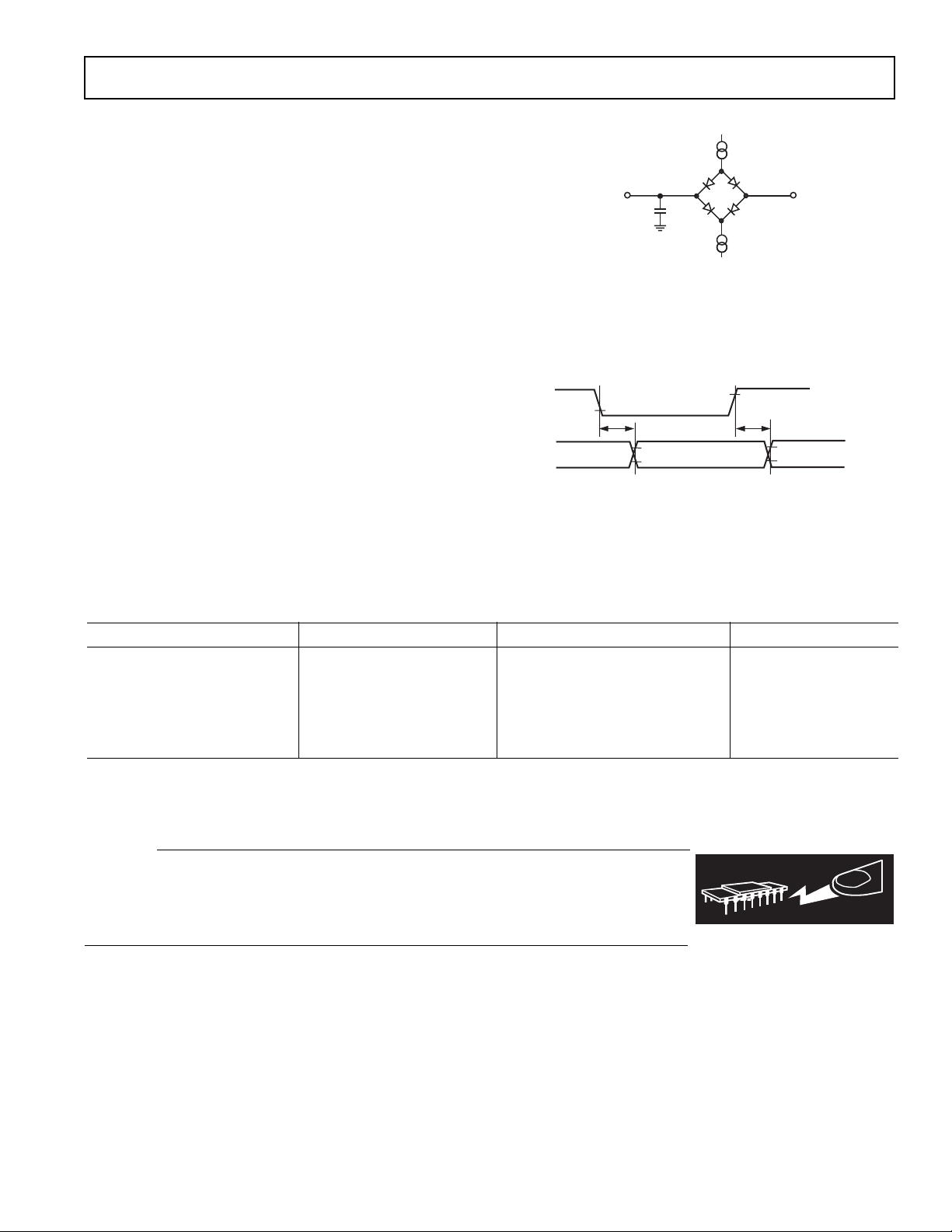
Figure 1. Load Circuit for Digital Interface Timing,
SDOUT, SYNC, SCLK Outputs, C
0.8V
t
DELAY
2V
0.8V
= 10 pF
L
2V
t
DELAY
2V
0.8V
Figure 2. Voltage Reference Levels for Timing
ORDERING GUIDE
Model Temperature Range Package Description Package Option
AD7678AST –40°C to +85°C Quad Flatpack (LQFP) ST-48
AD7678ASTRL –40°C to +85°C Quad Flatpack (LQFP) ST-48
AD7678ACP –40°C to +85°C Chip Scale (LFCSP) CP-48
AD7678ACPRL –40°C to +85°C Chip Scale (LFCSP) CP-48
EVAL-AD7678CB
EVAL-CONTROL BRD2
NOTES
1
This board can be used as a standalone evaluation board or in conjunction with the EVAL-CONTROL BRD2 for evaluation/demonstration
purposes.
2
This board allows a PC to control and communicate with all Analog Devices evaluation boards ending in the CB designators.
1
2
Evaluation Board
Controller Board
CAUTION
ESD (electrostatic discharge) sensitive device. Electrostatic charges as high as 4000 V readily
accumulate on the human body and test equipment and can discharge without detection. Although
the AD7678 features proprietary ESD protection circuitry, permanent damage may occur on devices
subjected to high-energy electrostatic discharges. Therefore, proper ESD precautions are
recommended to avoid performance degradation or loss of functionality.
REV. PrA
–5–
Page 6
AD7678
PRELIMINAR Y TECHNICAL DAT A
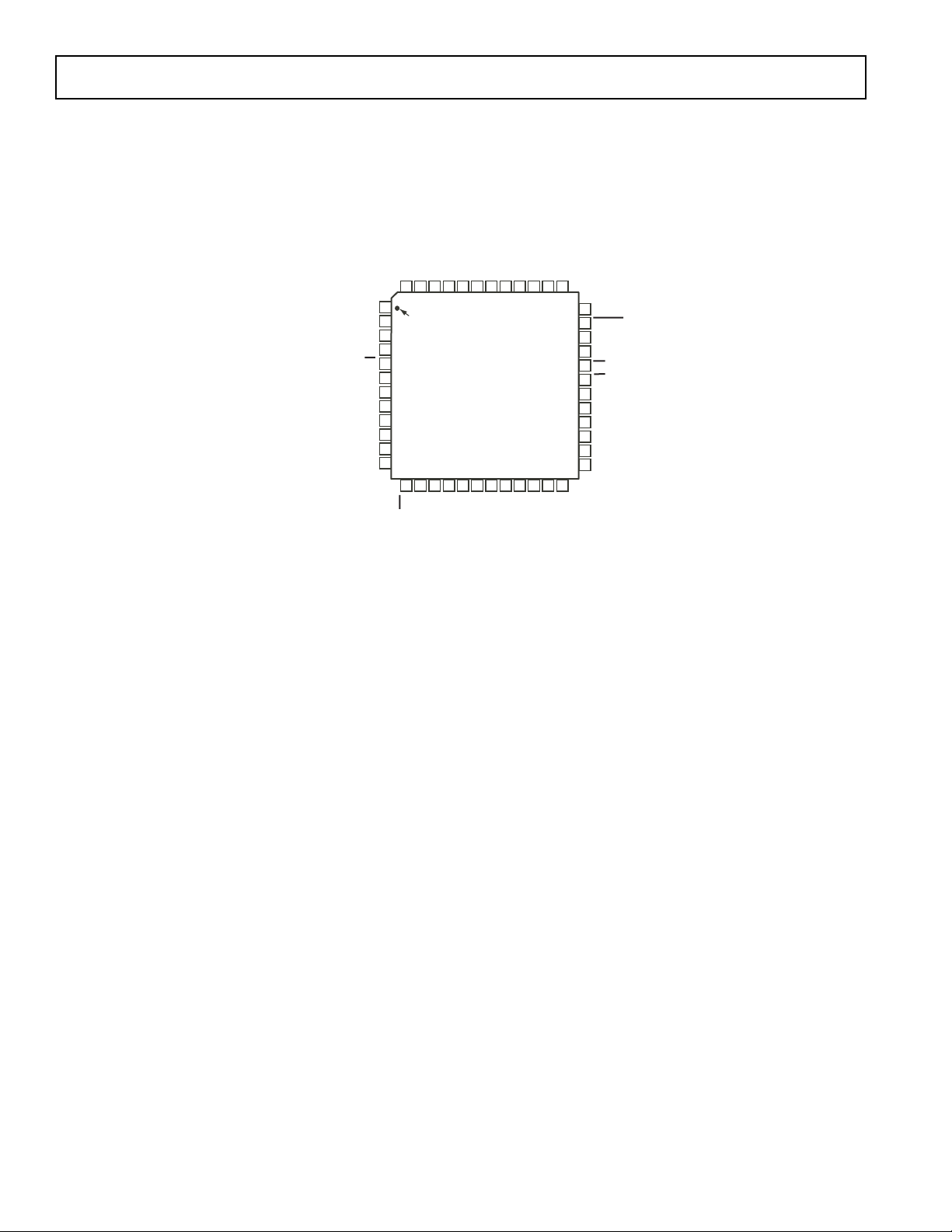
PIN CONFIGURATION
48-Lead LQFP
(ST-48)
PDBUF
AVDD
REFBUFINNCAGND
AGND
AVDD
MODE0
MODE1
D0/OB/2C
NC
NC
D1/A0
D2/A1
D3
D4/DIVSCLK[0]
D5/DIVSCLK[1]
NC = NO CONNECT
48
47 46
1
PIN 1
2
IDENTIFIER
3
4
5
6
7
8
9
10
11
12
13 14
15 16 17 18
IN+NCNCNCIN-
45 44 39 38 3743 42 41 40
AD7678
TOP VIEW
(Not to Scale)
19 20
21 22
REFGND
23 24
REF
36
35
34
33
32
31
30
29
28
27
26
25
AGND
CNVST
PD
RESET
CS
RD
DGND
BUSY
D17
D16
D15
D14
D6/EXT/INT
D8/INVSCLK
D7/INVSYNC
DVDD
OVDD
OGND
D9/RDC/SDIN
DGND
D10/SDOUT
D11/SCLK
D12/SYNC
D13/RDERROR
–6–
REV. PrA
Page 7

PRELIMINAR Y TECHNICAL DAT A
AD7678
PIN FUNCTION DESCRIPTIONS
Pin No. Mnemonic Type Description
1, 44 AGND P Analog Power Ground Pin.
2, 47 AVDD P Input Analog Power Pins. Nominally 5 V.
6-7, N C No Connect.
40–42,45
3 MODE0 DI Data Output Interface mode Selection.
4 MODE1 DI Data Output Interface mode Selection:
Interface MODE # MODE0 MODE1 Description
0 0 0 18-bit Interface
1 0 1 16-bit Interface
2 1 0 Byte Interface
3 1 1 Serial Interface
5 D0/OB/2C DI/O When MODE=0 (18 bit interface mode), this pin is Bit 0 of the parallel port data
output bus. In all other modes, this pin allows choice of Straight Binary/Binary Two’s
Complement.When OB/2C is HIGH, the digital output is straight binary; when
LOW, the MSB is inverted resulting in a two’s complement output from its internal
shift register.
8 D1/A0 D I /O When MODE=0 (18-bit interface mode), this pin is Bit 1 of the parallel port data
output bus. In all other modes, this input pin controls the form in which data is
output as shown in Table II.
9 D2/A 1 D I / O When MODE=0 or MODE=1 (18-bit or 16-bit interface mode), this pin is Bit 2 of
the parallel port data output bus. In all other modes, this input pin controls the form
in which data is output as shown in Table II.
10 D 3 D O In all MODES except MODE=3, this output is used as Bit 3 of the Parallel Port
Data Output Bus. This pin is always an output regard less of the interface mode.
11,12 DATA[4:5]or DI/O In all MODES except MODE=3, these pins are Bit 4 and Bit 5 of the Parallel
Port Data Output Bus.
DIVSCLK[0:1] In MODE=3 (serial mode), when EXT/INT is LOW, and RDC/SDIN is LOW,
which is serial master read after convert, these inputs, part of the serial port, are used
to slow down if desired the internal serial clock which clocks the data output. In other
serial modes, these pins are not used.
13 D 6 DI/O In all MODES except MODE=3, this output is used as Bit 6 of the Parallel Port
Data Output Bus.
or EXT/INT When MODE=3 (serial mode), this input, part of the serial port, is used as a digital
select input for choosing the internal or an external data clock. With EXT/INT tied
INT
LOW, the internal clock is selected on SCLK output. With EXT/
HIGH, output data is synchronized to an external clock signal connected to the
SCLK input.
14 D 7 DI/O In all MODES except MODE=3, this output is used as Bit 7 of the Parallel Port
Data Output Bus.
or INVSYNC When MODE=3 (serial mode), this input, part of the serial port, is used to select the
active state of the SYNC signal. When LOW, SYNC is active HIGH. When HIGH,
SYNC is active LOW.
15 D 8 DI/O In all MODES except MODE=3, this output is used as Bit 8 of the Parallel Port
Data Output Bus.
or INVSCLK When MODE=3 (serial mode), this input, part of the serial port, is used to invert the
SCLK signal. It is active in both master and slave mode.
16 D 9 DI/O In all MODES except MODE=3, this output is used as Bit 9 of the Parallel Port
Data Output Bus.
or RDC/SDIN When MODE=3 (serial mode), this input, part of the serial port, is used as either an
external data input or a read mode selection input depending on the state of
EXT/INT.
When EXT/INT is HIGH, RDC/SDIN could be used as a data input to daisy chain
the conversion results from two or more ADCs onto a single SDOUT line. The
digital data level on SDIN is output on DATA with a delay of 18 SCLK periods after
the initiation of the read sequence.
set to a logic
REV. PrA
–7–
Page 8

PRELIMINAR Y TECHNICAL DAT A
AD7678
Pin No. Mnemonic Type Description
When EXT/INT is LOW, RDC/SDIN is used to select the read mode. When
RDC/SDIN is HIGH, the data is output on SDOUT during conversion. When
RDC/SDIN is LOW, the data can be output on SDOUT only when the conversion is
complete.
17 OGND P Input/Output Interface Digital Power Ground.
18 OVDD P Input/Output Interface Digital Power. Nominally at the same supply than the supply
of the host interface (5 V or 3 V). Should not exceed DVDD by more than 0.3V.
19 DVDD P Digital Power. Nominally at 5 V.
20 DGND P Digital Power Ground.
21 D 1 0 D O In all MODES except MODE=3, this output is used as Bit 10 of the Parallel Port
Data Output Bus.
or SDOUT When MODE=3 (serial mode), this output, part of the serial port, is used as a serial
data output synchronized to SCLK. Conversion results are stored in an on-chip
register. The AD7678 provides the conversion result, MSB first, from its internal
shift register. The data format is determined by the logic level of OB/2C.
In serial mode, when EXT/INT is LOW, SDOUT is valid on both edges of SCLK.
In serial mode, when EXT/INT is HIGH:
If INVSCLK is LOW, SDOUT is updated on SCLK rising edge and valid on the
next falling edge.
If INVSCLK is HIGH, SDOUT is updated on SCLK falling edge and valid on the
next rising edge.
22 D 1 1 D I /O In all MODES except MODE=3, this output is used as the Bit 11 of the Parallel
Port Data Output Bus.
or SCLK When MODE=3 (serial mode), this pin, part of the serial port, is used as a serial
data clock input or output, dependent upon the logic state of the EXT/INT pin. The
active edge where the data SDOUT is updated depends upon the logic state of the
INVSCLK pin.
23 D 1 2 D O In all MODES except MODE=3, this output is used as the Bit 12 of the Parallel
Port Data Output Bus.
or SYNC When MODE=3 (serial mode), this output, part of the serial port, is used as a digital
output frame synchronization for use with the internal data clock (EXT/INT = Logic
LOW). When a read sequence is initiated and INVSYNC is LOW, SYNC is driven
HIGH and remains HIGH while SDOUT output is valid. When a read sequence is
initiated and INVSYNC is HIGH, SYNC is driven LOW and remains LOW while
SDOUT output is valid.
24 D 1 3 D O In all MODES except MODE=3, this output is used as the Bit 11 of the Parallel
Port Data Output Bus.
or RDERROR In MODE=3 (serial mode) and when EXT/INT is HIGH, this output, part of the
serial port, is used as a incomplete read error flag. In slave mode, when a data
read is started and not complete when the following conversion is complete, the
current data is lost and RDERROR is pulsed high.
25–28 DATA[14:17] D O Bit 14 to Bit 17 of the Parallel Port Data output bus. These pins are always outputs
regard less of the interface mode.
29 BUSY D O Busy Output. Transitions HIGH when a conversion is started, and remains HIGH
until the conversion is complete and the data is latched into the on-chip shift register.
The falling edge of BUSY could be used as a data ready clock signal.
30 DGND P Must be tied to digital ground.
31 RD DI
32 CS DI Chip Select. When CS and RD are both LOW, the interface parallel or serial output
33 RESET DI Reset Input. When set to a logic HIGH, reset the AD7678. Current conversion if any
34 P D D I Power-Down Input. When set to a logic HIGH, power consumption is reduced and
35 CNVST D I Start Conversion. If CNVST is held HIGH when the acquisition phase (t
Read Data. When CS and RD are both LOW, the interface parallel or serial output
bus is enabled.
bus is enabled. CS is also used to gate the external clock.
is aborted. If not used, this pin could be tied to DGND.
conversions are inhibited after the current one is completed.
) is com
plete, the next falling edge on CNVST puts the internal sample/hold into the hold
state and initiates a conversion. If CNVST is held LOW when the acquisition phase
) is complete, the internal sample/hold is put into the hold state and a conversion is
(t
8
immediately started.
8
–8–
REV. PrA
Page 9

PRELIMINAR Y TECHNICAL DAT A
AD7678
Pin No. Mnemonic Type Description
36 AGND P Must be tied to analog ground.
37 R EF AI Reference Input Voltage and Internal Reference Buffer Output. Apply an external
reference on this pin if the internal reference buffer is not used. Should be decoupled
effectively with or without the internal buffer.
38 REFGND AI Reference Input Analog Ground.
39 IN- AI Differential Negative Analog Input.
43 IN+ AI Differential Negative Analog Input.
46 REFBUFIN AI Reference Buffer Input Voltage. The internal reference buffer has a fixed gain. It
outputs 4.096V typically when 2.5V is applied on this pin.
48 PDBUF DI Allows choice of buffering reference. When LOW, the buffer is selected. When
HIGH, the buffer is switched off.
NOTES
AI = Analog Input
AI/O = Bidirectional Analog
AO = Analog Output
DI = Digital Input
DI/O = Bidirectional Digital
DO = Digital Output
P = Power
Table II. Data Bus Interface Definition
MODE MODE0 MODE1 D0/OB/
000R[0]R[1]R[2]R[3]R[4:9] R[10:11] R[12:15] R[16:17] 18-Bit Parallel
101OB/2C A0:0 R[2] R[3] R[4:9] R[10:11] R[12:15] R[16:17] 16-Bit High Word
101OB/2C A0:1 R [0] R[1 ] All Zeros 16-Bit Low Word
210OB/2C A0:0 A1:0 All Hi-Z R[10:11] R[12:15] R[16:17] 8-Bit HIGH Byte
210OB/2C A0:0 A1:1 All Hi-Z R[2:3] R[4:7] R[8:9] 8-Bit MID Byte
210OB/2C A0:1 A1:0 All Hi-Z R[0:1] All Zeros 8-Bit LOW Byte
210OB/2C A0:1 A1:1 All Hi-Z All Zeros R[0:1] 8-Bit LOW Byte
3 1 1 OB/2C All Hi-Z Serial Interface Serial Interface
R[0:17] is the 18-bit ADC value stored in its output register.
2C2C
2C D1/A0 D2/A1 D[3] D[4:9] D[10:11] D[12:15] D[16:17] DESCRIPTION
2C2C
REV. PrA
–9–
Page 10

AD7678
PRELIMINAR Y TECHNICAL DAT A
DEFINITION OF SPECIFICATIONS
INTEGRAL NONLINEARITY ERROR (INL)
Linearity error refers to the deviation of each individual
code from a line drawn from “negative full scale” through
“positive full scale”. The point used as “negative full
scale” occurs 1/2 LSB before the first code transition.
“Positive full scale” is defined as a level 1 1/2 LSB beyond
the last code transition. The deviation is measured from the
middle of each code to the true straight line.
DIFFERENTIAL NONLINEARITY ERROR (DNL)
In an ideal ADC, code transitions are 1 LSB apart. Differential nonlinearity is the maximum deviation from this
ideal value. It is often specified in terms of resolution for
which no missing codes are guaranteed.
Gain ERROR
The first transition (from 000 . . . 00 to 000 . . . 01)
should occur for an analog voltage 1/2 LSB above the
nominal –full scale (-4.095991 V for the ±4.096V range).
The last transition (from 111 . . . 10 to 111 . . . 11)
should occur for an analog voltage 1 1/2 LSB below the
nominal full scale (4.095977 V for the ±5V range). The
gain error is the deviation of the difference between the
actual level of the last transition and the actual level of the
first transition from the difference between the ideal levels.
ZERO ERROR
The zero error is the difference between the ideal midscale
input voltage (0 V) and the actual voltage producing the
midscale output code.
SPURIOUS FREE DYNAMIC RANGE (SFDR)
The difference, in decibels (dB), between the rms amplitude of the input signal and the peak spurious signal.
Effective number of bits (ENOB)
ENOB is a measurement of the resolution with a sine
wave input. It is related to S/(N+D) by the following formula:
ENOB = (S/[N+D]
and is expressed in bits.
TOTAL HARMONIC DISTORTION (THD)
THD is the ratio of the rms sum of the first five harmonic components to the rms value of a full-scale input
signal and is expressed in decibels.
SIGNAL-TO-NOISE RATIO (SNR)
SNR is the ratio of the rms value of the actual input signal
to the rms sum of all other spectral components below the
Nyquist frequency, excluding harmonics and dc. The
value for SNR is expressed in decibels.
SIGNAL TO (NOISE + DISTORTION) RATIO
(S/[N+D])
S/(N+D) is the ratio of the rms value of the actual input
signal to the rms sum of all other spectral components
below the Nyquist frequency, including harmonics but
excluding dc. The value for S/(N+D) is expressed in decibels.
APERTURE DELAY
Aperture delay is a measure of the acquisition performance
and is measured from the falling edge of the CNVST
input to when the input signal is held for a conversion.
TRANSIENT RESPONSE
The time required for the AD7678 to achieve its rated
accuracy after a full-scale step function is applied to its
input.
– 1.76)/6.02)
dB
–10–
REV. PrA
Page 11

PRELIMINAR Y TECHNICAL DAT A
CONVERSION CONTROL
Figure 11 shows the detailed timing diagrams of the conversion process. The AD7678 is controlled by the signal
CNVST which initiates conversion. Once initiated, it
cannot be restarted or aborted, even by the power-down
input PD, until the conversion is complete. The CNVST
signal operates independently of CS and RD signals.
t
2
t
1
CNVST
RESE
BUSY
DATA
AD7678
t
9
T
t
8
BUSY
t
3
t
5
MODE
ACQUIRE CONVERT ACQUIRE CONVERT
t
4
t
6
t
7
t
8
Figure 11. Basic Conversion Timing
For a true sampling application, the recommended operation of the CNVST signal is the following:
CNVST must be held high from the previous falling
edge of BUSY, and during a minimum delay corresponding to the acquisition time t8; then, when CNVST
is brought low, a conversion is initiated and BUSY signal
goes high until the completion of the conversion.
Although CNVST is a digital signal, it should be designed with this special care with fast, clean edges and
levels, with minimum overshoot and undershoot or ringing.
For applications where the SNR is critical, the CNVST
signal should have a very low jitter. Some solutions to
achieve that are to use a dedicated oscillator for CNVST
generation or, at least, to clock it with a high frequency
low jitter clock as shown in Figure 5.
For other applications, conversions can be automatically
initiated. If CNVST is held low when BUSY is low, the
AD7678 controls the acquisition phase and then automatically initiates a new conversion. By keeping CNVST low,
the AD7678 keeps the conversion process running by
itself. It should be noted that the analog input has to be
settled when BUSY goes low. Also, at power-up, CNVST
should be brought low once to initiate the conversion
process. In this mode, the AD7678 could sometimes run
slightly faster than the guaranteed limit of 100 kSPS.
CNVST
Figure 12. RESET Timing
DIGITAL INTERFACE
The AD7678 has a versatile digital interface; it can be
interfaced with the host system by using either a serial or
parallel interface. The serial interface is multiplexed on
the parallel data bus. The AD7678 digital interface also
accommodates both 3 V or 5 V logic by simply connecting the OVDD supply pin of the AD7678 to the host
system interface digital supply. Finally, except in 18 bit
interface mode, by using the OB/2C input pin, both
two’s complement or straight binary coding can be used.
The two signals CS and RD control the interface. When
at least one of these signals is high, the interface outputs
are in high impedance. Usually, CS allows the selection
of each AD7678 in multi-circuits applications and is
held low in a single AD7678 design. RD is generally
used to enable the conversion result on the data bus.
CS = RD = 0
t
1
CNVST
t
10
BUSY
DATA
BUS
t
3
PREVIOUS CONVERSION DATA NEW DATA
t
4
t
11
Figure 13. Master Parallel Data Timing for Reading
(Continuous Read)
REV. PrA
–11–
Page 12

AD7678
PRELIMINAR Y TECHNICAL DAT A
PARALLEL INTERFACE
The AD7678 is configured to use the parallel interface
with either a 18-bit, 16-bit or 8-bit bus width according to
the Table II. The data can be read either after each conversion, which is during the next acquisition phase, or
during the following conversion as shown, respectively, in
Figure 14 and Figure 15. When the data is read during
the conversion, however, it is recommended that it is read
only during the first half of the conversion phase. That
avoids any potential feedthrough between voltage transients
on the digital interface and the most critical analog conversion circuitry. Please refer to table II for a detailed
description of the different options available.
CS
RD
BUSY
DATA
BUS
t
12
CURRENT
CONVERSION
t
13
CS = 0
t
3
1
PREVIOUS
CONVERSION
t
t
4
13
CNVST, RD
BUSY
DATA
BUS
t
t
12
Figure 15. Slave Parallel Data Timing for Reading
(Read During Convert)
SERIAL INTERFACE
The AD7678 is configured to use the serial interface when
MODE0 and MODE1 are held high. The AD7678 outputs 18 bits of data, MSB first, on the SDOUT pin. This
data is synchronized with the 18 clock pulses provided on
SCLK pin. The output data is valid on both the rising and
falling edge of the data clock.
Figure 14. Slave Parallel Data Timing for Reading
(Read After Convert)
CS, RD
CNVST
BUSY
SYNC
SCLK
SDOUT
t
3
t
t
14
t
15
t
16
EXT/INT = 0 RDC/SDIN = 0 INVSCLK = INVSYNC = 0
29
t
20
123 161718
X
t
D17 D16 D2 D1 D0
22
t
28
t
30
t
25
t
18
t
19
t
21
t
23
t
24
t
26
t
27
Figure 16. Master Serial Data Timing for Reading (Read After Convert)
–12–
REV. PrA
Page 13

PRELIMINAR Y TECHNICAL DAT A
AD7678
MASTER SERIAL INTERFACE
Internal Clock
The AD7678 is configured to generate and provide the serial
data clock SCLK when the EXT/INT pin is held low.
The AD7678 also generates a SYNC signal to indicate to
the host when the serial data is valid. The serial clock
SCLK and the SYNC signal can be inverted if desired.
Depending on RDC/SDIN input, the data can be read
after each conversion or during the following conversion.
Figure 16 and Figure 17 show the detailed timing diagrams of these two modes.
Usually, because the AD7678 has a longer acquisition
phase than the conversion phase, the data is read immediately after conversion. That makes the mode master, read
after conversion, the most recommended serial mode when
it can be used.
In read-after-conversion mode, it should be noted that,
unlike in other modes, the signal BUSY returns low after
the 18 data bits are pulsed out and not at the end of the
conversion phase which results in a longer BUSY width.
To accomodate slow digital hosts, the serial clock can be
slowed down by using DIVSCLK.
In read-during-conversion mode, the serial clock and data
toggle at appropriate instants which minimize potential
feedthrough between digital activity and the critical conversion decisions.
SLAVE SERIAL INTERFACE
External Clock
The AD7678 is configured to accept an externally supplied serial data clock on the SCLK pin when the EXT/
INT pin is held high. In this mode, several methods can
be used to read the data. The external serial clock is
gated by CS. When CS and RD are both low, the data
can be read after each conversion or during the following
conversion. The external clock can be either a continuous
or discontinuous clock. A discontinuous clock can be
either normally high or normally low when inactive. Figure 18 and Figure 20 show the detailed timing diagrams of
these methods. Usually, because the AD7676 has a longer
acquisition phase than the conversion phase, the data are
read immediately after conversion.
While the AD7678 is performing a bit decision, it is important that voltage transients not occur on digital input/
output pins or degradation of the conversion result could
occur. This is particularly important during the second
half of the conversion phase because the AD7678 provides
error correction circuitry that can correct for an improper bit decision made during the first half of the
conversion phase. For this reason, it is recommended
that when an external clock is being provided, it is a
discontinuous clock that is toggling only when BUSY is
low or, more importantly, that it does not transition during the latter half of BUSY high.
EXT/INT = 0 RDC/SDIN = 1 INVSCLK = INVSYNC = 0
CS, RD
t
CNVST
BUSY
SYNC
SCLK
SDOUT
t
t
14
t
15
t
16
1
t
3
17
t
19
t20 t
21
12 3 161718
t
18
D17 D16 D2 D1 D0X
t
t
22
23
t
24
Figure 17. Master Serial Data Timing for Reading (Read Previous Conversion During Convert)
t
25
t
26
t
27
REV. PrA
–13–
Page 14

AD7678
PRELIMINAR Y TECHNICAL DAT A
External Discontinuous Clock Data Read After Conversion
This mode is the most recommended of the serial slave
modes. Figure 18 shows the detailed timing diagrams of
this method. After a conversion is complete, indicated by
BUSY returning low, the result of this conversion can be
read while both CS and RD are low. The data is shifted
out, MSB first, with 18 clock pulses and is valid on both
rising and falling edge of the clock.
Among the advantages of this method, the conversion
performance is not degraded because there are no voltage
transients on the digital interface during the conversion
process.
Another advantage is to be able to read the data at any
speed up to 40 MHz which accommodates both slow
digital host interface and the fastest serial reading.
EXT/INT = 1 INVSCLK = 0
CS
BUSY
t
35
t36 t
37
Finally, in this mode only, the AD7678 provides a
“daisy-chain” feature using the RDC/SDIN input pin for
cascading multiple converters together. This feature is
useful for reducing component count and wiring connections when desired as, for instance, in isolated
multiconverter applications.
An example of the concatenation of two devices is shown
in Figure 19. Simultaneous sampling is possible by using
a common CNVST signal. It should be noted that the
RDC/SDIN input is latched on the edge of SCLK opposite
to the one used to shift out the data on SDOUT. Hence, the
MSB of the “upstream” converter just follows the LSB of
the “downstream” converter on the next SCLK cycle.
= 0
RD
SCLK
SDOUT
CS
CNVST
BUSY
SCLK
SDOUT
1 2 3 14151617 18
t
SDIN
31
X
D17 D16 D1
t
16
X17 X16 X15 X1 X0 Y17 Y16
t
33
t
32
D15
t
34
Figure 18. Slave Serial Data Timing for Reading (Read After Convert)
EXT/INT = 1 INVSCLK = 0
t
3
t
16
t
35
t36 t
37
123 161718
t
31
X
D17 D16 D15
t
32
D1
RD =0
D0
D0
X17 X16
Figure 20. Slave Serial Data Timing for Reading (Read Previous Conversion During Convert)
–14–
REV. PrA
Page 15

PRELIMINAR Y TECHNICAL DAT A
BUSY
OUT
BUSYBUSY
AD7678
AD7678
(UPSTREAM)
RDC/SDIN SDOUT
SCLK IN
CS IN
CNVST IN
#2
CNVST
CS
SCLK
AD7678
#1
(DOWNSTREAM)
SDOUTRDC/SDIN
CNVST
SCLK
CS
DATA
OUT
Figure 19. Two AD7667s in a “Daisy-Chain” Configuration
External Clock Data Read During Conversion
Figure 20 shows the detailed timing diagrams of this
method. During a conversion, while both CS and RD are
both low, the result of the previous conversion can be
read. The data is shifted out, MSB first, with 18 clock
pulses and is valid on both rising and falling edge of the
clock. The 18 bits have to be read before the current conversion is complete. If that is not done, RDERROR is
pulsed high and can be used to interrupt the host interface to prevent incomplete data reading. There is no
“daisy chain” feature in this mode and RDC/SDIN
input should always be tied either high or low.
To reduce performance degradation due to digital activity,
a fast discontinuous clock of is recommended to ensure that
all the bits are read during the first half of the conversion
phase. It is also possible to begin to read the data after
conversion and continue to read the last bits even after a new
conversion has been initiated.
REV. PrA
–15–
Page 16

AD7678
PRELIMINAR Y TECHNICAL DAT A
APPLICATION HINTS
Layout
The AD7678 has very good immunity to noise on the
power supplies. However, care should still be taken with
regard to grounding layout.
The printed circuit board that houses the AD7678
should be designed so the analog and digital sections
are separated and confined to certain areas of the board.
This facilitates the use of ground planes that can be
easily separated. Digital and analog ground planes
should be joined in only one place, preferably underneath the AD7678, or, at least, as close as possible to the
AD7678. If the AD7678 is in a system where multiple
devices require analog to digital ground connections,
the connection should still be made at one point only, a
star ground point, which should be established as close
as possible to the AD7678.
It is recommended to avoid running digital lines under the
device as these will couple noise onto the die. The analog
ground plane should be allowed to run under the
AD7678 to avoid noise coupling. Fast switching signals
like CNVST or clocks should be shielded with digital
ground to avoid radiating noise to other sections of the
board, and should never run near analog signal paths.
Crossover of digital and analog signals should be
avoided. Traces on different but close layers of the board
should run at right angles to each other. This will reduce
the effect of feedthrough through the board. The power
supply lines to the AD7678 should use as large a trace as
possible to provide low impedance paths and reduce the
effect of glitches on the power supply lines. Good decoupling is also important to lower the supplies impedance
presented to the AD7678 and reduce the magnitude of
the supply spikes. Decoupling ceramic capacitors, typically 100 nF, should be placed on each power supplies
pins AVDD, DVDD and OVDD close to, and ideally
right up against these pins and their corresponding
ground pins. Additionally, low ESR 10 µF capacitors
should be located in the vicinity of the ADC to further
reduce low frequency ripple.
The DVDD supply of the AD7678 can be either a
separate supply or come from the analog supply,
AVDD, or from the digital interface supply, OVDD.
When the system digital supply is noisy, or fast switching
digital signals are present, it is recommended if no separate supply available, to connect the DVDD digital
supply to the analog supply AVDD through an RC filter
as shown in Figure 5, and connect the system supply to the
interface digital supply OVDD and the remaining digital
circuitry. When DVDD is powered from the system supply, it is useful to insert a bead to further reduce
high-frequency spikes.
The AD7678 has four different ground pins; REFGND,
AGND, DGND, and OGND. REFGND senses the reference voltage and should be a low impedance return to
the reference because it carries pulsed currents. AGND
is the ground to which most internal ADC analog signals are referenced. This ground must be connected with
the least resistance to the analog ground plane. DGND
must be tied to the analog or digital ground plane depend-
ing on the configuration. OGND is connected to the
digital system ground.
The layout of the decoupling of the reference voltage is
important. The decoupling capacitor should be close to
the ADC and connected with short and large traces to
minimize parasitic inductances.
Evaluating the AD7678 Performance
A recommended layout for the AD7678 is outlined in the
documentation of the evaluation board for the AD7678.
The evaluation board package includes a fully assembled and tested evaluation board, documentation,
and software for controlling the board from a PC via
the Eval-Control BRD2.
–16–
REV. PrA
Page 17

PRELIMINAR Y TECHNICAL DAT A
D
OUTLINE DIMENSIONS
Dimensions shown in inches and (mm).
48-Lead Quad Flatpack (LQFP)
(ST-48)
0.063 (1.60)
0.030 (0.75)
MAX
0.018 (0.45)
0.354 (9.00) BSC SQ
48
1
37
36
AD7678
0.276 (7.0)
BSC SQ
PIN 1
INDICATOR
VIEW
COPLANARITY
TOP
0.003 (0.08)
0.008 (0.2)
0.004 (0.09)
0
MIN
7
0
TOP VIEW
(PINS DOWN)
12
13
0.019 (0.5)
BSC
0.006 (0.15)
0.002 (0.05)
0.011 (0.27)
0.006 (0.17)
SEATING
PLANE
25
24
0.276
(7.00)
BSC
SQ
0.057 (1.45)
0.053 (1.35)
48-Lead Frame Chip Scale Package (LFCSP)
(CP-48)
0.024 (0.60)
0.017 (0.42)
0.009 (0.24)
37
36
BOTTOM
VIEW
48
1
0.266 (6.75)
BSC SQ
0.024 (0.60)
0.017 (0.42)
0.009 (0.24)
0.215 (5.45)
0.209 (5.30) SQ
0.203 (5.15)
REV. PrA
12 MAX
0.039 (1.00) MAX
0.033 (0.85) NOM
0.020 (0.50)
0.016 (0.40)
0.031 (0.80) MAX
0.026 (0.65) NOM
0.020 (0.50)
BSC
0.008 (0.20)
REF
CONTROLLING DIMENSIONS ARE IN MILLIMETERS
0.012 (0.30)
0.002 (0.05)
0.0004 (0.01)
0.0 (0.0)
–17–
25
24
0.012 (0.30)
0.009 (0.23)
0.007 (0.18)
12
13
Paddle connected to AGN
 Loading...