

Page 1
LC2MOS
a
FEATURES
2 ms ADC with Track/Hold
1 ms DAC with Output Amplifier
AD7569, Single DAC Output
AD7669, Dual DAC Output
On-Chip Bandgap Reference
Fast Bus Interface
Single or Dual 5 V Supplies
GENERAL DESCRIPTION
The AD7569/AD7669 is a complete, 8-bit, analog I/O system
on a single monolithic chip. The AD7569 contains a high speed
successive approximation ADC with 2 µs conversion time, a track/
hold with 200 kHz bandwidth, a DAC and an output buffer amplifier with 1 µs settling time. A temperature-compensated 1.25 V
bandgap reference provides a precision reference voltage for the
ADC and the DAC. The AD7669 is similar, but contains two
DACs with output buffer amplifiers.
A choice of analog input/output ranges is available. Using a supply voltage of +5 V, input and output ranges of zero to 1.25 V
and zero to 2.5 volts may be programmed using the RANGE input pin. Using a ±5 V supply, bipolar ranges of ±1.25 V or
±2.5 V may be programmed.
Digital interfacing is via an 8-bit I/O port and standard microprocessor control lines. Bus interface timing is extremely fast, allowing easy connection to all popular 8-bit microprocessors. A
separate start convert line controls the track/hold and ADC to
give precise control of the sampling period.
The AD7569/AD7669 is fabricated in Linear-Compatible
CMOS (LC
combining precision bipolar circuits with low power CMOS
logic. The AD7569 is packaged in a 24-pin, 0.3" wide “skinny”
DIP, a 24-terminal SOIC and 28-terminal PLCC and LCCC
packages. The AD7669 is available in a 28-pin, 0.6" plastic
DIP, 28-terminal SOIC and 28-terminal PLCC package.
2
MOS), an advanced, mixed technology process
Complete, 8-Bit Analog I/0 Systems
AD7569/AD7669
AD7569 FUNCTIONAL BLOCK DIAGRAM
AD7669 FUNCTIONAL BLOCK DIAGRAM
PRODUCT HIGHLIGHTS
1. Complete Analog I/O on a Single Chip.
The AD7569/AD7669 provides everything necessary to
interface a microprocessor to the analog world. No external
components or user trims are required and the overall accuracy of the system is tightly specified, eliminating the need
to calculate error budgets from individual component
specifications.
2. Dynamic Specifications for DSP Users.
In addition to the traditional ADC and DAC specifications,
the AD7569/AD7669 is specified for ac parameters, including signal-to-noise ratio, distortion and input bandwidth.
3. Fast Microprocessor Interface.
The AD7569/AD7669 has bus interface timing compatible
with all modern microprocessors, with bus access and relinquish times less than 75 ns and write pulse width less than
80 ns.
REV. B
Information furnished by Analog Devices is believed to be accurate and
reliable. However, no responsibility is assumed by Analog Devices for its
use, nor for any infringements of patents or other rights of third parties
which may result from its use. No license is granted by implication or
otherwise under any patent or patent rights of Analog Devices.
One Technology Way, P.O. Box 9106, Norwood, MA 02062-9106, U.S.A.
Tel: 617/329-4700 World Wide Web Site: http://www.analog.com
Fax: 617/326-8703 © Analog Devices, Inc., 1996
Page 2

AD7569/AD7669–SPECIFICATIONS
(VDD = +5 V 6 5%; V
DAC SPECIFICATIONS
Parameter J Version Versions S Version T Version Units Conditions/Comments
STATIC PERFORMANCE
Resolution
Total Unadjusted Error
Relative Accuracy
Differential Nonlinearity
Unipolar Offset Error DAC data is all 0s; V
Bipolar Zero Offset Error DAC data is all 0s; V
Full-Scale Error
4
5
5
5
@ +25°C ± 2 ±1.5 ±2 ±1.5 LSB max Typical tempco is 10 µV/°C for +1.25 V range
T
to T
MIN
MAX
@ +25°C ± 2 ±1 5 ±2 ±1.5 LSB max Typical tempco is 20 µV/°C for ±1.25 V range
T
to T
MIN
MAX
6
(AD7569 Only) VDD = 5 V
1
unless otherwise noted. All specifications T
AD7569
J, A Versions
AD7669 K, B AD7569 AD7569
8 8 8 8 Bits
± 2 ± 2 ± 3 ± 3 LSB typ
± 1 ± 1/2 ±1 ±1/2 LSB max
± 1 ± 3/4 ±1 ±3/4 LSB max Guaranteed Monotonic
±2.5 ±2 ±2.5 ±2 LSB max
±2.5 ±2 ±2.5 ±2 LSB max
3
AD7569
2
= RANGE = AGND
SS
= AGND
DAC
MIN
= DGND = 0 V; RL = 2 kV, CL = 100 pF to AGND
ADC
to T
unless otherwise noted.)
MAX
= 0 V
SS
= –5 V
SS
DAC
@ +25°C ± 2 ±1 ±2 ±1 LSB max
T
to T
MIN
Full-Scale Error
MAX
6
(AD7669 Only) VDD = 5 V
±3 ±2 ±4 ±3 LSB max
@ +25°C ± 3 LSB max
T
to T
MIN
DACA/DACB Full-Scale Error Match
MAX
±4.5 LSB max
6
(AD7669 Only) ± 2.5 LSB max VDD = 5 V
∆Full Scale/∆V
∆Full Scale/∆V
Load Regulation at Full Scale 0.2 0.2 0.2 0.2 LSB max RL = 2 kΩ to °/C
DYNAMIC PERFORMANCE
Signal-to-Noise Ratio
Total Harmonic Distortion
Intermodulation Distortion5 (IMD) 55 55 55 55 dB typ fa = 18.4 kHz, fb = 14.5 kHz with f
, TA = +25°C 0.5 0.5 0.5 0.5 LSB max V
DD
, TA = +25°C 0.5 0.5 0.5 0.5 LSB max V
SS
5
(SNR) 44 46 44 46 dB min V
5
(THD) 48 48 48 48 dB max V
= 2.5 V; ∆VDD = ±5%
OUT
= –2.5 V; ∆VSS = ±5%
OUT
= 20 kHz full-scale sine wave with f
OUT
= 20 kHz full-scale sine wave with f
OUT
SAMPLING
SAMPLING
SAMPLING
= 400 kHz
= 400 kHz
= 400 kHz
ANALOG OUTPUT
Output Voltage Ranges
Unipolar 0 to +1.25/2.5 Volts V
Bipolar ±1.25/±2.5 Volts VDD = +5 V, VSS = –5 V
LOGIC INPUTS
CS, X/B,WR, RANGE, RESET, DB0–DB7
Input Low Voltage, V
Input High Voltage, V
Input Leakage Current 10 10 10 10 µA max V
Input Capacitance
DB0–DB7
Input Coding (Single Supply) Binary
INL
INH
7
0.8 0.8 0.8 0.8 V max
2.4 2.4 2.4 2.4 V min
10 10 10 10 pF max
= +5 V, VSS = 0 V
DD
= 0 to V
IN
DD
Input Coding (Dual Supply) 2s Complement
AC CHARACTERlSTICS
Voltage Output Settling Time Settling time to within ±1/2 LSB of final value
7
Positive Full-Scale Change 2 2 2 2 µs max Typically 1 µs
Negative Full-Scale Change (Single Supply) 4 4 4 4 µs max Typically 2 µs
Negative Full-Scale Change (Dual Supply) 2 2 2 2 µs max Typically 1 µs
Digital-to-Analog Glitch Impulse
Digital Feedthrough
to V
V
IN
OUT
DAC to DAC Crosstalk
5
Isolation 60 60 60 60 dB typ VIN = ±2.5 V, 50 kHz Sine Wave
5
15 15 15 15 nV secs typ
1 1 1 1 nV secs typ
5
(AD7669 Only) 1 nV secs typ
DACA to DACB Isolation5 (AD7669 Only) –70 dB max
POWER REQUIREMENTS
V
Range 4.75/5.25 4.75/5.25 4.75/5.25 4.75/5.25 V min/V max For Specified Performance
DD
Range (Dual Supplies) –4.75/–5.25 –4.75/–5.25 –4.75/–5.25 –4.75/–5.25 V min/V max Specified Performance also applies to VSS = 0 V
V
SS
I
DD
(AD7569) 13 13 13 13 mA max Output unloaded
for unipolar ranges.
V
= VIN = 2.5 V; Logic Inputs = 2.4 V; CLK = 0.8 V
OUT
(AD7669) 18 mA max Outputs unloaded
I
(Dual Supplies) V
SS
(AD7569) 4 4 4 4 mA max Output unloaded
= VIN = –2.5 V; Logic Inputs = 2.4 V; CLK = 0.8 V
OUT
(AD7669) 6 mA max Outputs unloaded
DAC/ADC MATCHING
Gain Matching
@ +25°C 1 111% typ20 kHz sine wave
T
MIN
NOTES
1
Specifications apply to both DACs in the AD7669. V
2
Except where noted, specifications apply for all output ranges including bipolar ranges with dual supply operation.
3
Temperature ranges as follows: J, K versions; 0°C to +70°C
4
1 LSB = 4.88 mV for 0 V to +1.25 V output range, 9.76 mV for 0 V to +2.5 V and ±1.25 V ranges and 19.5 mV for ±2.5 V range.
5
See Terminology.
6
Includes internal voltage reference error and is calculated after offset error has been adjusted out. Ideal unipolar full-scale voltage is (FS – 1 LSB); ideal bipolar positive full-scale voltage is (FS/2 – 1 LSB)
and ideal bipolar negative full-scale voltage is –FS/2.
7
Sample tested at +25°C to ensure compliance.
Specifications subject to change without notice.
to T
MAX
6
VIN to V
match with VIN = ±2.5 V,
OUT
1 111% typ
applies to both V
OUT
A, B versions; –40°C to +85°C
S, T versions; –55°C to +125°C
OUT
A and V
B of the AD7669.
OUT
–2–
REV. B
Page 3
AD7569/AD7669
AD7569
1
= RANGE = AGND
SS
= AGND
DAC
= DGND = 0 V; f
DAC
VDD = 5 V
= ±2.5 V, dc to 200 kHz sine wave
IN
= +5 V; VSS = 0 V
DD
= +5 V; VSS = –5 V
DD
= 0 to V
IN
= 1.6 mA
SINK
SOURCE
= 5 MHz
CLK
DD
DD
= 200 µA
= 5 MHz external unless other-
CLK
SAMPLING
SAMPLING
= 400 kHz
SAMPLING
ADC SPECIFICATIONS
wise noted. All specifications T
Parameter J Version Versions S Version T Version Units Conditions/Comments
DC ACCURACY
DYNAMIC PERFORMANCE
ANALOG INPUT
LOGIC INPUTS
LOGIC OUTPUTS
CONVERSION TIME
3
Resolution
Total Unadjusted Error
Relative Accuracy
Differential Nonlinearity
Unipolar Offset Error Typical tempco is 10 µV/°C for +1.25 V range; V
@ +25°C ±2 ±1.5 ±2 ± 1.5 LSB max
T
to T
MIN
Bipolar Zero Offset Error Typical tempco is 20 µV/°C for + 1.25 V range; V
Full-Scale Error
∆Full Scale/∆V
∆Full Scale/∆VSS, TA = +25°C 0.5 0.5 0.5 0.5 LSB max VIN = –2.5 V; ∆VSS = ± 5%
Signal-to-Noise Ratio
Total Harmonic Distortion4 (THD) 48 48 48 48 dB max VIN = 100 kHz full-scale sine wave with f
Intermodulation Distortion4 (IMD) 60 60 60 60 dB typ fa = 99 kHz, fb = 96.7 kHz with f
Frequency Response 0.1 0.1 0.1 0.1 dB typ V
Track/Hold Acquisition Time
Input Voltage Ranges
Input Current ±300 ± 300 ±300 ±300 µA max See equivalent circuit Figure 5
Input Capacitance 10 10 10 10 pF typ
CS, RD, ST, CLK, RESET, RANGE
CS, RD, ST, RANGE, RESET
CLK
DB0–DB7,
DB0–DB7
Output Coding (Single Supply) Binary
Output Coding (Dual Supply) 2s Complement
With External Clock 2 2 2 2 µs max f
With Internal Clock, T
MAX
@ +25°C ±3 ±2.5 ±3 ± 2.5 LSB max
T
to T
MIN
@ +25°C –4, +0 –4, +0 –4, +0 –4, +0 LSB max
T
to T
MIN
MAX
Unipolar 0 to +1.25/ +2.5 Volts V
Bipolar ± 1.25/±2.5 Volts V
Input Low Voltage, V
Input High Voltage, V
Input Capacitance
Input Leakage Current 10 10 10 10 µA max V
Input Current
I
INL
I
INH
INT, BUSY
VOL, Output Low Voltage 0.4 0.4 0.4 0.4 V max I
V
, Output High Voltage 4.0 4.0 4.0 4.0 V min I
OH
Floating State Leakage Current 10 10 10 10 µA max
Floating State Output Capacitance
4
4
4
MAX
5
, TA = +25°C 0.5 0.5 0.5 0.5 LSB max VIN = +2.5 V; ∆VDD = ±5%
DD
4
(SNR) 44 46 44 45 dB min VIN = 100 kHz full-scale sine wave with f
7
INL
INH
8
8
= +25°C 1.6 1.6 1.6 1.6 µs min Using recommended clock components shown in Figure 21.
A
(VDD = +5 V 6 5%; V
to T
MIN
unless otherwise noted.) Specifications apply to Mode 1 interface.
MAX
AD7569
J, A Versions
AD7669 K, B AD7569 AD7569
8 8 8 8 Bits
± 3 ± 3 ±4 ±4 LSB typ
± 1 ± 1/2 ± 1 ± 1/2 LSB max
± 1 ± 3/4 ± 1 ± 3/4 LSB max No Missing Codes
3
± 3 ±2.5 ± 3 ±2.5 LSB max
±3.5 ±3 ±4 ± 3.5 LSB max
–5.5, +1.5 –5.5, +1.5 –7.5, +2 –7.5, +2 LSB max
200 200 300 300 ns typ
0.8 0.8 0.8 0.8 V max
2.4 2.4 2.4 2.4 V min
10 10 10 10 pF max
–1.6 –1.6 –1.6 –1.6 mA max VIN = 0 V
40 40 40 40 µA max VIN = V
10 10 10 10 pF max
2.6 2.6 2.6 2.6 µs max Clock frequency can be adjusted by varying R
= 0 V
SS
SS
= 400 kHz
= 400 kHz
.
CLK
= –5 V
6
6
POWER REQUIREMENTS As per DAC Specifications
NOTES
1
Except where noted, specifications apply for all ranges including bipolar ranges with dual supply operation.
2
Temperature ranges are as follows: J, K versions; 0°C to +70°C
3
1 LSB = 4.88 mV for 0 V to +1.25 V range, 9.76 mV for 0 V to +2.5 V and ±1.25 V ranges and 19.5 mV for +2.5 V range.
4
See Terminology.
5
Includes internal voltage reference error and is calculated after offset error has been adjusted out. Ideal unipolar last code transition occurs at (FS – 3/2 LSB). Ideal bipolar last code transition occurs at
(FS/2 – 3/2 LSB).
6
Exact frequencies are 101 kHz and 384 kHz to avoid harmonics coinciding with sampling frequency.
7
Rising edge of BUSY to falling edge of ST. The time given refers to the acquisition time, which gives a 3 dB degradation in SNR from the tested figure.
8
Sample tested at +25°C to ensure compliance.
Specifications subject to change without notice.
REV. B
A, B versions; –40°C to +85°C
S, T versions; –55°C to +125°C
–3–
Page 4
1
WARNING!
ESD SENSITIVE DEVICE
AD7569/AD7669–TIMING CHARACTERISTICS
(See Figures 8, 10, 12; VDD = 5 V 6 5%; VSS = 0 V or –5 V 6 5%)
Limit at Limit at
Limit at T
MIN
, T
MAX
T
, T
MIN
MAX
Parameter 258C (All Grades) (J, K, A, B Grades) (S, T Grades) Units Test Conditions/Comments
DAC Timing
t
1
t
2
t
3
t
4
t
5
80 80 90 ns min WR Pulse Width
0 0 0 ns min CS, A/B to WR Setup Time
0 0 0 ns min CS, A/B to WR Hold Time
60 70 80 ns min Data Valid to WR Setup Time
10 10 10 ns min Data Valid to WR Hold Time
ADC Timing
t
6
t
7
t
8
t
9
t
10
t
11
t
12
2
t
13
3
t
14
50 50 50 ns min ST Pulse Width
110 130 150 ns max ST to BUSY Delay
20 30 30 ns max BUSY to INT Delay
0 0 0 ns min BUSY to CS Delay
0 0 0 ns min CS to RD Setup Time
60 75 90 ns min RD Pulse Width Determined by t13.
0 0 0 ns min CS to RD Hold Time
60 75 90 ns max Data Access Time after RD; CL = 20 pF
95 120 135 ns max Data Access Time after
RD; CL = 100 pF
10 10 10 ns min Bus Relinquish Time after RD
60 75 85 ns max
t
15
t
16
2
t
17
65 75 85 ns max RD to INT Delay
120 140 160 ns max RD to BUSY Delay
60 75 90 ns max Data Valid Time after BUSY; CL = 20 pF
90 115 135 ns max Data Valid Time after BUSY; CL = 100 pF
NOTES
1
Sample tested at +25°C to ensure compliance. All input control signals are specified with tR = tF = 5 ns (10% to 90% of +5 V) and timed from a voltage level of 1.6 V.
2
t13 and t17 are measured with the load circuits of Figure 1 and defined as the time required for an output to cross either 0.8 V or 2.4 V.
3
tl4 is defined as the time required for the data line to change 0.5 V when loaded with the circuit of Figure 2.
Specifications subject to change without notice.
a. High-Z to V
OH
Figure 1. Load Circuits for Data Access Time Test
ABSOLUTE MAXIMUM RATINGS
VDD to AGND
V
to DGND . . . . . . . . . . . . . . . . . . . . . . . . . . .–0.3 V, +7 V
DD
V
to VSS . . . . . . . . . . . . . . . . . . . . . . . . . . . . . –0.3 V, +14 V
DD
AGND
AGND
or AGND
DAC
to AGND
DAC
or AGND
DAC
ADC
to DGND . . . . –0.3 V, VDD + 0.3 V
ADC
. . . . . . . . . . . . . . . . . . . . . . . . . ±5 V
ADC
Logic Voltage to DGND . . . . . . . . . . . . . –0.3 V, V
CLK Input Voltage to DGND . . . . . . . . . –0.3 V, V
V
(V
OUT
1
A, V
DAC
OUT
AGND
V
to AGND
IN
NOTE
1
Output may be shorted to any voltage in the range VSS to VDD provided that the
power dissipation of the package is not exceeded. Typical short circuit current for
a short to AGND or VSS is 50 mA.
B) to
OUT
. . . . . . . . . . . . . . . . . VSS – 0.3 V, VDD + 0.3 V
. . . . . . . . . . . . . . . VSS – 0.3 V, VDD + 0.3 V
ADC
b. High-Z to V
OL
. . . . . . . . . . . . . –0.3 V, +7 V
+ 0.3 V
DD
+ 0.3 V
DD
a. VOH to High-Z b. VOL to High-Z
Figure 2. Load Circuits for Bus Relinquish Time Test
Power Dissipation (Any Package) to +75°C . . . . . . . . 450 mW
Derates above 75°C by . . . . . . . . . . . . . . . . . . . . . 6 mW/°C
Operating Temperature Range
Commercial (J, K) . . . . . . . . . . . . . . . . . . . . . . 0°C to +70°C
Industrial (A, B) . . . . . . . . . . . . . . . . . . . . . –40°C to +85°C
Extended (S, T) . . . . . . . . . . . . . . . . . . . . –55°C to +125°C
Storage Temperature Range . . . . . . . . . . . . –65°C to +150°C
Lead Temperature (Soldering, 10 secs) . . . . . . . . . . . +300°C
*Stresses above those listed under “Absolute Maximum Ratings” may cause
permanent damage to the device. This is a stress rating only; functional operation
of the device at these or any other condition above those indicated in the
operational sections of this specification is not implied. Exposure to absolute
maximum rating conditions for extended periods may affect device reliability.
CAUTION
ESD (electrostatic discharge) sensitive device. Electrostatic charges as high as 4000 V readily
accumulate on the human body and test equipment and can discharge without detection.
Although the AD7569/AD7669 features proprietary ESD protection circuitry, permanent damage may occur on devices subjected to high energy electrostatic discharges. Therefore, proper
ESD precautions are recommended to avoid performance degradation or loss of functionality.
–4–
REV. B
Page 5

AD7569/AD7669
NOTE:
The term DAC (Digital-to-Analog Converter) throughout the
data sheet applies equally to the dual DACs in the AD7669 as
well as to the single DAC of the AD7569 unless otherwise
stated. It follows that the term V
V
B of the AD7669 also.
OUT
TERMINOLOGY
Total Unadjusted Error
applies to both V
OUT
OUT
A and
Total unadjusted error is a comprehensive specification that includes internal voltage reference error, relative accuracy, gain
and offset errors.
Relative Accuracy (DAC)
Relative Accuracy or endpoint nonlinearity is a measure of the
maximum deviation from a straight line passing through the
endpoints of the DAC transfer function. It is measured after allowing for offset and gain errors. For the bipolar output ranges,
the endpoints of the DAC transfer function are defined as those
voltages that correspond to negative full-scale and positive fullscale codes. For the unipolar output ranges, the endpoints are
code 1 and code 255. Code 1 is chosen because the amplifier is
now working in single supply and, in cases where the true offset
of the amplifier is negative, it cannot be seen at code 0. If the
relative accuracy were calculated between code 0 and code 255,
the “negative offset” would appear as a linearity error. If the offset is negative and less than 1 LSB, it will appear at code 1, and
hence the true linearity of the converter is seen between code 1
and code 255.
Relative Accuracy (ADC)
Relative Accuracy is the deviation of the ADC’s actual code
transition points from a straight line drawn between the endpoints of the ADC transfer function. For the bipolar input
ranges, these points are the measured, negative, full-scale transition point and the measured, positive, full-scale transition point.
For the unipolar ranges, the straight line is drawn between the
measured first LSB transition point and the measured full-scale
transition point.
Differential Nonlinearity
Differential Nonlinearity is the difference between the measured
change and an ideal 1 LSB change between any two adjacent
codes. A specified differential nonlinearity of ± 1 LSB max ensures monotonicity (DAC) or no missed codes (ADC). A differential nonlinearity of ±3/4 LSB max ensures that the minimum
step size (DAC) or code width (ADC) is 1/4 LSB, and the maximum step size or code width is 3/4 LSB.
Digital-to-Analog Glitch Impulse
Digital-to-Analog Glitch Impulse is the impulse injected into the
analog output when the digital inputs change state with the
DAC selected. It is normally specified as the area of the glitch in
nV secs and is measured when the digital input code is changed
by 1 LSB at the major carry transition.
Digital Feedthrough
Digital Feedthrough is also a measure of the impulse injected to
the analog output from the digital inputs, but is measured when
the DAC is not selected. It is essentially feedthrough across the
die and package. It is also a measure of the glitch impulse transferred to the analog output when data is read from the internal
ADC. It is specified in nV secs and is measured with
WR high
and a digital code change from all 0s to all 1s.
DAC-to-DAC Crosstalk (AD7669 Only)
The glitch energy transferred to the output of one DAC due to
an update at the output of the second DAC. The figure given is
the worst case and is expressed in nV secs. It is measured with
an update voltage of full scale.
DAC-to-DAC Isolation (AD7669 Only)
DAC-to-DAC Isolation is the proportion of a digitized sine
wave from the output of one DAC, which appears at the output
of the second DAC (loaded with all 1s). The figure given is the
worst case for the second DAC output and is expressed as a ratio in dBs. It is measured with a digitized sine wave (f
SAMPLING
=
100 kHz) of 20 kHz at 2.5 V pk-pk.
Signal-to-Noise Ratio
Signal-to-Noise Ratio (SNR) is the measured signal to noise at
the output of the converter. The signal is the rms magnitude of
the fundamental. Noise is the rms sum of all the nonfundamental signals (excluding dc) up to half the sampling frequency.
SNR is dependent on the number of quantization levels used in
the digitization process; the more levels, the smaller the quantization noise. The theoretical SNR for a sine wave is given by
SNR = (6.02N + 1.76) dB
where N is the number of bits. Thus for an ideal 8-bit converter,
SNR = 50 dB.
Harmonic Distortion
Harmonic Distortion is the ratio of the rms sum of harmonics to
the fundamental. For the AD7569/AD7669, Total Harmonic
Distortion (THD) is defined as
2
2
2
2
2
+V
5
6
20 log
+V
+V
V
2
3
+V
4
V
1
where V1 is the rms amplitude of the fundamental and V2, V3,
V
, V5 and V6 are the rms amplitudes of the individual
4
harmonics.
Intermodulation Distortion
With inputs consisting of sine waves at two frequencies, fa and
fb, any active device with nonlinearities will create distortion
products, of order (m + n), at sum and difference frequencies of
mfa ± nfb where m, n = 0, l, 2, 3,… . Intermodulation terms
are those for which m or n is not equal to zero. For example,
the second order terms include (fa + fb) and (fa – fb) and the
third order terms include (2fa + fb), (2fa – fb), (fa + 2fb) and
(fa – 2fb).
REV. B
–5–
Page 6
AD7569/AD7669
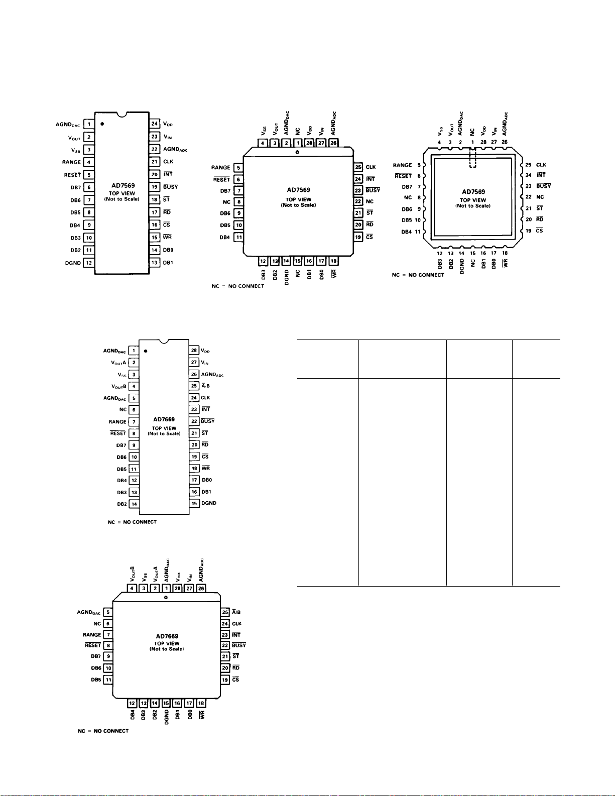
AD7569 PIN CONFIGURATIONS
DIP, SOIC
AD7669 PIN CONFIGURATIONS
DIP, SOIC
PLCC
PLCC
LCCC
ORDERING GUIDE
Relative
Temperature Accuracy Package
Model Range T
MIN –TMAX
Option
AD7569JN 0°C to +70°C ±1 LSB N-24
AD7569JR 0°C to +70°C ±1 LSB R-24
AD7569AQ –40°C to +85°C ±1 LSB Q-24
AD7569SQ
2
–55°C to +125°C ±1 LSB Q-24
AD7569BN –40°C to +85°C ±0.5 LSB N-24
AD7569KN 0°C to +70°C ±0.5 LSB N-24
AD7569BR –40°C to +85°C ±0.5 LSB R-24
AD7569BQ –40°C to +85°C ±0.5 LSB Q-24
AD7569TQ
AD7569JP 0°C to +70°C ±1 LSB P-28A
AD7569SE
AD7569KP 0°C to +70°C ±1/2 LSB P-28A
AD7569TE
2
–55°C to +125°C ±1/2 LSB Q-24
2
–55°C to +125°C ±1 LSB E-28A
2
–55°C to +125°C ±1/2 LSB E-28A
AD7669AN –40°C to +85°C ±1 LSB N-28
AD7669JN 0°C to +70°C ±1 LSB N-28
AD7669JP 0°C to +70°C ±1 LSB P-28A
AD7669AR –40°C to +85°C ±1 LSB R-28
AD7669JR 0°C to +70°C ±1 LSB R-28
NOTES
1
E = Leadless Ceramic Chip Carrier; N = Plastic DIP; P = Plastic Leaded Chip
Carrier; Q = Cerdip; R = Small Outline SOIC.
2
To order MIL-STD-883, Class B processed parts, add /883B to part number.
Contact your local sales office for military data sheet.
1
–6–
REV. B
Page 7

PIN FUNCTION DESCRIPTION
(Applies to the AD7569 and AD7669 unless otherwise stated.)
AD7569/AD7669
Pin
Mnemonic Description
AGND
DAC
Analog Ground for the DAC(s). Separate
ground return paths are provided for the
DAC(s) and ADC to minimize crosstalk.
V
(V
OUT
OUT
A, V
OUT
Output Voltage. V
B) voltage from the AD7569 DAC. V
V
B are the buffered DAC output voltages
OUT
is the buffered output
OUT
OUT
A and
from the AD7669. Four different output voltage ranges can be achieved (see Table I).
V
SS
Negative Supply Voltage (–5 V for dual supply or 0 V for single supply). This pin is also
used with the RANGE pin to select the different input/output ranges and changes the data
format from binary (V
ment (V
= –5 V) (see Table I).
SS
= 0 V) to 2s comple-
SS
RANGE Range Selection Input. This is used with the
V
input to select the different ranges as per
SS
Table I. The range selected applies to both
the analog input voltage of the ADC and the
output voltage from the DAC(s).
RESET Reset Input (Active Low). This is an asyn-
chronous system reset that clears the DAC
register(s) to all 0s and clears the
INT line of
the ADC (i.e., makes the ADC ready for new
conversion). In unipolar operation, this input
sets the output voltage to 0 V; in bipolar
operation, it sets the output to negative full
scale.
DB7 Data Bit 7. Most Significant Bit (MSB).
DB6–DB2 Data Bit 6 to Data Bit 2.
DGND Digital Ground.
DB1 Data Bit 1.
DB0 Data Bit 0. Least Significant Bit (LSB).
WR Write Input (Edge triggered). This is used in
conjunction with
CS to write data into the
AD7569 DAC register. It is used in conjunction with
CS and A/B to write data into the
selected DAC register of the AD7669. Data is
transferred on the rising edge of WR.
Pin
Mnemonic Description
CS Chip Select Input (Active Low). The device is
selected when this input is active.
RD READ Input (Active Low). This input must
be active to access data from the part. In the
Mode 2 interface,
version. It is used in conjunction with the
RD going low starts con-
CS
input (see Digital Interface Section).
ST Start Conversion (Edge triggered). This is
used when precise sampling is required. The
falling edge of
ST starts conversion and drives
BUSY low. The ST signal is not gated with
CS.
BUSY BUSY Status Output (Active Low). When
this pin is active, the ADC is performing a
conversion. The input signal is held prior to
the falling edge of
BUSY (see Digital Inter-
face Section).
INT INTERRUPT Output (Active Low). INT go-
ing low indicates that the conversion is complete.
INT goes high on the rising edge of CS
or
RD and is also set high by a low pulse on
RESET (see Digital Interface Section).
A/B (AD7669 DAC Select Input. This input selects which
Only) DAC register data is written to under control
of
CS and WR. With this input low, data is
written to the DACA register; with this input
high, data is written to the DACB register.
CLK A TTL compatible clock signal may be used
to determine the ADC conversion time. Internal clock operation is achieved by connecting
a resistor and capacitor to ground.
AGND
V
IN
ADC
Analog Ground for the ADC.
Analog Input. Various input ranges can be se-
lected (see Table I).
V
DD
Positive Supply Voltage (+5 V).
REV. B
Table I. Input/Output Ranges
Input/Output DB0–DB7
Range V
SS
Voltage Range Data Format
0 0 V 0 V to +1.25 V Binary
1 0 V 0 V to +2.5 V Binary
0 –5 V ±1.25 V 2s Complement
1 –5 V ±2.5 V 2s Complement
–7–
Page 8

AD7569/AD7669—Typical Performance Graphs
Noise Spectral Density vs. Frequency
Positive-Going Settling Time (±2.5 V Range)
Power Supply Rejection Ratio vs. Frequency
Negative-Going Settling Time (±2.5 V Range)
DAC/ADC Full-Scale Temperature Coefficient
–8–
IMD Plot for ADC
REV. B
Page 9

AD7569/AD7669
CIRCUIT DESCRIPTION
D/A SECTION
The AD7569 contains an 8-bit, voltage-mode, D/A converter
that uses eight equally weighted current sources switched into
an R-2R ladder network to give a direct but unbuffered 0 V to
+1.25 V output range. The AD7669 is similar, but contains two
D/A converters. The current sources are fabricated using PNP
transistors. These transistors allow current sources that are
driven from positive voltage logic and give a zero-based output
range. The output voltage from the voltage switching R-2R ladder network has the same positive polarity as the reference;
therefore, the D/A converter can be operated from a single
power supply rail.
The PNP current sources are generated using the on-chip
bandgap reference and a control amplifier. The current sources
are switched to either the ladder or AGND
by high speed
DAC
p-channel switches. These high-speed switches ensure a fast settling time for the output voltage of the DAC. The R-2R ladder
network of the DAC consists of highly stable, thin-film resistors.
A simplified circuit diagram for the D/A converter section is
shown in Figure 3. An identical D/A converter is used as part of
the A/D converter, which is discussed later.
Figure 3. DAC Simplified Circuit Diagram
OP AMP SECTION
The output from the D/A converter is buffered by a high speed,
noninverting op amp. This op amp is capable of developing
±2.5 V across a 2 kΩ and 100 pF load to AGND
. The am-
DAC
plifier can be operated from a single +5 V supply to give two
unipolar output ranges, or from dual supplies (± 5 V) to allow
two bipolar output ranges.
The feedback path of the amplifier contains a gain/offset network that provides four voltage ranges at the output of the op
amp. The output voltage range is determined by the RANGE
and V
inputs. (See Table I in the Pin Function Description
SS
section.) The four possible output ranges are: 0 V to +1.25 V,
0 V to +2.5 V, ±1.25 V and ±2.5 V. It should be noted that
whichever range is selected for the output amplifier also applies
to the input voltage range of the A/D converter.
The output amplifier settles to within 1/2 LSB of its final value
in typically less than 500 ns. Operating the part from single or
dual supplies has no effect on the positive-going settling time.
However, the negative-going output settling time to voltages
near 0 V in single supply will be slightly longer than the settling
time to negative full scale for dual supply operation. Additionally, to ensure that the output voltage can go to 0 V in single
supply, a transistor on the output acts as a passive pull-down
with output voltages near 0 V with V
= 0 V. This means that
SS
the sink capability of the amplifier is reduced as the output voltage nears 0 V in single supply. In dual supply operation the full
sink capability of 1.25 mA is maintained over the entire output
voltage range.
For all other parameters, the single and dual supply performances of the amplifier are essentially identical. The output
noise from the amplifier, with full scale on the DAC, is 200 µV
peak-to-peak. The spot noise at 1 kHz is 35 nV/√
Hz with all 0s
on the DAC. A noise spectral density versus frequency plot for
the amplifier is shown in the typical performance graphs.
VOLTAGE REFERENCE
The AD7569/AD7669 contains an on-chip bandgap reference
that provides a low noise, temperature compensated reference
voltage for both the DAC and the ADC. The reference is
trimmed for absolute accuracy and temperature coefficient. The
bandgap reference is generated with respect to V
. It is buff-
DD
ered by a separate control amplifier for both the DAC and the
ADC reference. This can be seen in the DAC ladder network
configuration in Figure 3.
DIGITAL SECTION
The data pins on the AD7569/AD7669 provide a connection
between the external bus and DAC data inputs and ADC data
outputs. The threshold levels of all digital inputs and outputs
are compatible with either TTL or 5 V CMOS levels. Internal
input protection of all digital pins is achieved by on-chip distributed diodes.
The data format is straight binary when the part is used in single
supply (V
= 0 V). However, when a VSS of –5 V is applied, the
SS
data format becomes twos complement. This data format applies to the digital inputs of the DAC and the digital outputs of
the ADC.
ADC SECTION
The analog-to-digital converter on the AD7569/AD7669 uses
the successive approximation technique to achieve a fast conversion time of 2 µs and provides an 8-bit parallel digital output.
The reference for the ADC is provided by the on-chip bandgap
reference.
Conversion start is controlled by
ST or by CS and RD. Once a
conversion has been started, another conversion start should not
be attempted until the conversion in progress is completed.
Exercising the
RESET input does not affect conversion; the
RESET input resets the INT line high, which is useful in inter-
rupt driven systems where a READ has not been performed at
the end of the previous conversion. The
INT line does not have
to be cleared at the end of conversion. The ADC will continue
to convert correctly, but the function of the
INT line will be
affected.
Figure 4 shows the operating waveforms for a conversion cycle.
The analog input voltage, V
ing edge of
ST or (CS & RD). The MSB decision is made ap-
, is held 50 ns typical after the fall-
IN
proximately 50 ns after the second falling edge of the input
CLK following a conversion start. If t
in Figure 4 is greater
1
than 50 ns, then the falling edge of the input CLK will be seen
as the first falling clock edge. If t
is less than 50 ns, the first fall-
1
ing clock edge of the conversion will not occur until one clock
cycle later. The succeeding bit decisions are made approximately 50 ns after a CLK edge until conversion is complete.
REV. B
–9–
Page 10

AD7569/AD7669
At the end of conversion, the SAR contents are transferred to
the output latch, and the SAR is reset in readiness for a new
conversion. A single conversion lasts for 8 input clock cycles.
Figure 4. Operating Waveforms Using External Clock
ANALOG INPUT
The analog input of the AD7569/AD7669 feeds into an on-chip
track-and-hold amplifier. To accommodate different full-scale
ranges, the analog input signal is conditioned by a gain/offset
network that conditions all input ranges so the internal ADC always works with a 0 V to +1.25 V signal. As a result, the input
current on the V
input varies with the input range selected as
IN
shown in Figure 5.
INTERNAL CLOCK
Clock pulses are generated by the action of an internal current
source charging the external capacitor (C
capacitor discharging through the external resistor (R
) and this external
CLK
CLK
).
When a conversion is complete, this internal clock stops operating and the CLK pin goes to the DGND potential. Connections
for R
CLK
and C
are shown in the operating diagram of Fig-
CLK
ure 21. The nominal conversion time versus temperature for the
recommended R
CLK
and C
combination is shown in Figure
CLK
6. The internal clock provides a convenient clock source for the
AD7569/AD7669. Due to process variations, the actual operating frequency for this R
CLK/CCLK
combination can vary from
device to device by up to ±25%.
Figure 5. Equivalent VIN Circuit
TRACK-AND-HOLD
The track-and-hold (T/H) amplifier on the analog input of the
AD7569/AD7669 allows the ADC to accurately convert an input sine wave of 2.5 V peak-to-peak amplitude up to a frequency of 200 kHz, the Nyquist frequency of the ADC when
operated at its maximum throughput rate of 400 kHz. This
maximum rate of conversion includes conversion time and time
between conversions. Because the input bandwidth of the T/H
amplifier is much larger than 200 kHz, the input signal should
be band-limited to avoid converting high-frequency noise
components.
The operation of this T/H amplifier is essentially transparent to
the user. The T/H amplifier goes from its tracking mode to its
hold mode at the start of conversion. This occurs when the
ADC receives a conversion start command from either
ST or
CS & RD. At the end of conversion (BUSY going high), the
T/H reverts back to tracking the input signal.
EXTERNAL CLOCK
The AD7569/AD7669 ADC can be used with its on-chip clock
or with an externally applied clock. When using an external
clock, the CLK input of the AD7569/AD7669 may be driven
directly from 74HC, 4000B series buffers (such as 4049) or
from TTL buffers. When conversion is complete, the internal
clock is disabled. The external clock can continue to run between conversions without being disabled. The mark/space ratio
of the external clock can vary from 70/30 to 30/70.
Figure 6. Conversion Time vs. Temperature for Internal
Clock Operation
DIGITAL INTERFACE
DAC Timing and Control—AD7569
Table II shows the truth table for DAC operation for the
AD7569. The part contains an 8-bit DAC register, which is
loaded from the data bus under control of
CS and WR. The
data contained in the DAC register determines the analog output from the DAC. The
WR input is an edge-triggered input,
and data is transferred into the DAC register on the rising edge
of
WR. Holding CS and WR low does not make the DAC regis-
ter transparent.
Table II. AD7569 DAC Truth Table
CS WR RESET DAC Function
H H H DAC Register Unaffected
L L H DAC Register Unaffected
L g H DAC Register Updated
g L H DAC Register Updated
X X L DAC Register Loaded with All Zeros
L = Low State, H = High State, X = Don’t Care
The contents of the DAC register are reset to all 0s by an active
low pulse on the
the output remains at 0 V after
polar output ranges, a low pulse on
go to negative full scale.
RESET line, and for the unipolar output ranges,
RESET returns high. For the bi-
RESET causes the output to
In unipolar applications, the RESET line
can be used to ensure power-up to 0 V on the AD7569 DAC output and is also useful when used as a zero override in system calibration cycles. If the
RESET input is connected to the system
–10–
REV. B
Page 11

AD7569/AD7669
RESET line, the DAC output resets to 0 V when the entire
system is reset. Figure 7 shows the input control logic for the
AD7569 DAC; the write cycle timing diagram is shown in
Figure 8.
Figure 7. AD7569 DAC Input Control Logic
The contents of the DAC registers are reset to all 0s by an active
low pulse on the
ranges, the outputs remain at 0 V after
For the bipolar output ranges, a low pulse on
outputs to go to negative full scale. In unipolar applications, the
RESET line can be used to ensure power-up to 0 V on the
AD7669 DAC outputs and is also useful when used as a zero
override in system calibration cycles. If the
nected to the system
to 0 V when the entire system is reset. Figure 9 shows the DAC
input control logic for the AD7669, and the write cycle timing
diagram is shown in Figure 8.
RESET line, and for the unipolar output
RESET returns high.
RESET causes the
RESET input is con-
RESET line, then the DAC outputs reset
Figure 8. AD7569/AD7669 Write Cycle Timing Diagram
DAC Timing and Control—AD7669
Table III shows the truth table for the dual DAC operation of
the AD7669. The part contains two 8-bit DAC registers that are
loaded from the data bus under the control of
Address line
loaded to. The data contained in the DAC registers determines
the analog output from the respective DACs. The
an edge-triggered input, and data is transferred into the selected
DAC register on the rising edge of
low does not make the selected DAC register transparent. The
A/B input should not be changed while CS and WR are low.
CS WR A/B RESET DAC Function
H H X H DAC Registers Unaffected
L g L H DACA Register Updated
g L L H DACA Register Updated
L g H H DACB Register Updated
g L H H DACB Register Updated
X X X L DAC Registers Loaded with
L = Low State, H = High State, X = Don’t Care
A/B selects which DAC register the data is
WR. Holding CS and WR
Table III. AD7669 DAC Truth Table
All Zeros
CS, A/B and WR.
WR input is
Figure 9. AD7669 DAC Control Logic
ADC Timing and Control
The ADC on the AD7569/AD7669 is capable of two basic operating modes. In the first mode, the
version and drive the track-and-hold into hold mode. At the end
of conversion, the track-and-hold returns to its tracking mode.
The second mode is achieved by hard-wiring the
In this case,
sor is driven into a WAIT state for the duration of conversion by
BUSY.
CS and RD start conversion, and the microproces-
Figure 10. ADC Mode 1 Interface Timing
ST line is used to start con-
ST line high.
REV. B
–11–
Page 12

AD7569/AD7669
MODE 1 INTERFACE
The timing diagram for the first mode is shown in Figure 10. It
can be used in digital signal processing and other applications
where precise sampling in time is required. In these applications, it is important that the signal sampling occurs at exactly
equal intervals to minimize errors due to sampling uncertainty
or jitter. In these cases, the
ST line is driven by a timer or some
precise clock source.
The falling edge of the
ST pulse starts conversion and drives the
AD7569/AD7669 track-and-hold amplifier into its hold mode.
BUSY stays low for the duration of conversion and returns high
at the end of conversion and the track-and hold amplifier reverts
to its tracking mode on this rising edge of
BUSY. The INT line
can be used to interrupt the microprocessor. A READ to the
AD7569/AD7669 address accesses the data, and the
reset on the rising edge of
be used to trigger a pulse that drives the
CS or RD. Alternatively, the INT can
CS and RD and places
INT line is
the data into a FIFO or buffer memory. The microprocessor can
then read a batch of data from the FIFO or buffer memory at
some convenient time. The
ST input should not be high when
RD is brought low; otherwise, the part will not operate correctly
in this mode.
It is important, especially in systems where the conversion start
(
ST pulse) is asynchronous to the microprocessor, that a READ
does not occur during a conversion. Trying to read data from
the device during a conversion can cause errors to the conversion in progress. Also, pulsing the
ST line a second time before
conversion ends should be avoided since it too can cause errors
in the conversion result. In applications where precise sampling
is not critical, the
cessor
WR or RD line gated with a decoded address (different
from AD7569/AD7669
ST pulse can be generated from a micropro-
CS address).
Figure 11. Multichannel Inputs
This interface mode is also useful in applications where a number of input channels are required to be converted by the ADC.
Figure 11 shows the circuit configuration for such an application. The signal that drives the
ST input of the AD7569/
AD7669 is also used to drive the ENABLE input of the multiplexer. The multiplexer is enabled on the rising edge of the
ST
pulse while the input signal is held on the falling edge; therefore,
the signal must have settled to within 8 bits over the duration of
this
ST pulse. The settling time, including t
(ENABLE) of
ON
the multiplexer plus the T/H acquisition time (typically 200 ns),
thus determines the width of the
ST pulse. This is suited to applications where a number of input channels needs to be successively sampled or scanned.
MODE 2 INTERFACE
The second interface mode is intended for use with microprocessors, which can be forced into a WAIT state for at least 2 µs.
The
ST line of the AD7569/AD7669 must be hardwired high to
achieve this mode. The microprocessor starts a conversion and
is halted until the result of the conversion is read from the converter. Conversion is initiated by executing a memory READ to
the AD7569/AD7669 address, bringing
CS and RD low. BUSY
subsequently goes low (forcing the microprocessor READY or
WAIT input low), placing the microprocessor into a WAIT
state. The input signal is held on the falling edge of
ing
CS is already low or is coincident with RD). When the con-
version is complete (
BUSY goes high), the processor completes
RD (assum-
the memory READ and acquires the newly converted data.
While conversion is in progress, the ADC places old data (from
the previous conversion) on the data bus. The timing diagram
for this interface is shown in Figure 12.
Figure 12. ADC Mode 2 Interface Timing
The major advantage of this interface is that it allows the microprocessor to start conversion, WAIT, and then READ data with
a single READ instruction. The user does not have to worry
about servicing interrupts or ensuring that software delays are
long enough to avoid reading during conversion. The fast conversion time of the ADC ensures that for many microprocessors,
the processor is not placed in a WAIT state for an excessive
amount of time.
DIGITAL SIGNAL PROCESSING APPLICATIONS
In Digital Signal Processing (DSP) application areas such as
voice recognition, echo cancellation and adaptive filtering, the
dynamic characteristics (SNR, Harmonic Distortion, Intermodulation Distortion) of both the ADC and DAC are critical. The
AD7569/AD7669 is specified dynamically as well as with standard dc specifications. Because the track/hold amplifier has a
wide bandwidth, an antialiasing filter should be placed on the
V
input to avoid aliasing of high-frequency noise back into the
IN
band of interest.
The dynamic performance of the ADC is evaluated by applying a
sine-wave signal of very low distortion to the V
input, which is
IN
sampled at a 409.6 kHz sampling rate. A Fast Fourier Transform
(FFT) plot or Histogram plot is then generated from which SNR,
harmonic distortion and dynamic differential nonlinearity data
can be obtained. For the DAC, the codes for an ideal sine wave
are stored in PROM and loaded down to the DAC. The output
spectrum is analyzed, using a spectrum analyzer to evaluate SNR
–12–
REV. B
Page 13

and harmonic distortion performance. Similarly, for intermodulation distortion, an input (either to V
or DAC code)
IN
consisting of pure sine waves at two frequencies is applied to the
AD7569/AD7669.
Figure 13. ADC FFT Plot
Figure 13 shows a 2048 point FFT plot of the ADC with an input signal of 130 kHz. The SNR is 48.4 dB. It can be seen that
most of the harmonics are buried in the noise floor. It should be
noted that the harmonics are taken into account when calculating the SNR. The relationship between SNR and resolution (N)
is expressed by the following equation:
SNR = (6.02N + 1.76) dB
This is for an ideal part with no differential or integral linearity
errors. These errors will cause a degradation in SNR. By working backward from the above equation, it is possible to get a
measure of ADC performance expressed in effective number of
bits (N). This effective number of bits is plotted versus frequency in Figure 14. The effective number of bits typically falls
between 7.7 and 7.8, corresponding to SNR figures of 48.1 dB
and 48.7 dB.
Figure 15 shows a spectrum analyzer plot of the output spectrum from the DAC with an ideal sine-wave table loaded to the
data inputs of the DAC. In this case, the SNR is 46 dB.
AD7569/AD7669
Figure 15. DAC Output Spectrum
HISTOGRAM PLOT
When a sine wave of specified frequency is applied to the VIN input of the AD7569/AD7669 and several thousand samples are
taken, it is possible to plot a histogram showing the frequency of
occurrence of each of the 256 ADC codes. If a particular step is
wider than the ideal 1 LSB width, the code associated with that
step will accumulate more counts than for the code for an ideal
step. Likewise, a step narrower than ideal width will have fewer
counts. Missing codes are easily seen because a missing code
means zero counts for a particular code. The absence of large
spikes in the plot indicates small differential nonlinearity.
Figure 16 shows a histogram plot for the ADC indicating very
small differential nonlinearity and no missing codes for an input
frequency of 204 kHz. For a sine-wave input, a perfect ADC
would produce a cusp probability density function described by
the equation
π(A
1
2−V2)1/ 2
p(V ) =
where A is the peak amplitude of the sine wave and p(V) the
probability of occurrence at a voltage V.
The histogram plot of Figure 16 corresponds very well with this
cusp shape.
Further typical plots of the performance of the AD7569/AD7669
are shown in the Typical Performance Graphs section of the data
sheet.
Figure 14. Effective Number of Bits vs. Frequency
REV. B
Figure 16. ADC Histogram Plot
–13–
Page 14

AD7569/AD7669
INTERFACING THE AD7569/AD7669
AD7569/AD7669—Z80 INTERFACE
Figure 17 shows a typical interface to the Z80 microprocessor.
The ADC is configured for operation in the Mode 1 interface
mode. A precise timer or clock source starts conversion in applications requiring equidistant sampling intervals. The scheme
used, whereby
rupt on the Z80, is limited in that it does not allow the ADC to
be sampled at the maximum rate. This is because the time between samples has to be long enough to allow the Z80 to service
its interrupt and read data from the ADC. To overcome this,
some buffer memory or FIFO could be placed between the
AD7569/AD7669 and the Z80. Writing data to the relevant
AD7569/AD7669 DAC simply consists of a <LD (nn), A> instruction where nn is the decoded address for that DAC. Reading data from the ADC, after an
consists of a < LDA, (nn)> instruction.
AD7569/AD7669—68008 INTERFACE
A typical interface to the 68008 is shown in Figure 18. In this
case, the ADC is configured in the Mode 2 interface mode. This
means that the one read instruction starts conversion and reads
the data. The read cycle is stretched out over the entire conversion period by taking the
of the 68008. The additional gates are required so the 68008
receives a
AD7569/AD7669. In this case, there are no wait states introduced into the write cycle. Writing data to the relevant AD7569/
AD7669 DAC consists of a <MOVE.B Dn, addr> where Dn is
the data register, which contains the data to be loaded to that
DAC, and addr is the decoded address for the DAC. Data is
read from the ADC using a <MOVE.B addr,Dn> with the conversion result placed in register Dn.
INT of the AD7569/AD7669 generates an inter-
INT has been received,
Figure 17. AD7569/AD7669 to Z80 Interface
INT line back into the DTACK input
DTACK when the processor is writing data to the
AD7569/AD7669—ADSP-2100 INTERFACE
Figure 19 shows a typical interface to the DSP processor, the
ADSP-2100. The ADC is in the Mode 2 interface mode, which
means that the ADSP-2100 is halted during conversion. This is
achieved using the decoded address output. This is gated with
DMWR to ensure that it halts the processor for READ instructions only.
processor and allows it to finish off the READ instruction.
Because the instruction cycle of the ADSP-2100 is so fast
(125 ns cycle), the
for write cycles. This is achieved using the 74121, which generates a pulse that is fed back to DMACK. The duration of this
pulse determines how long the ADSP-2100 write cycle is
stretched. The buffers driving the DMACK line must have
open-collector outputs. Writing data to the relevant AD7569/
AD7669 DAC is achieved using a single instruction, <DM
(addr) = MRO>, where addr is the decoded address of that
DAC, and MRO contains the data to be loaded to the DAC register. Data is read from the ADC also, using a single instruction
<MRO = DM (addr)>, where the conversion result is placed in
the MRO data register.
AD7569/AD7669—IBM PC* INTERFACE
The AD7569/AD7669 is ideal for implementing an analog input/output port for the IBM PC. Figure 20 shows an interface
that realizes this function. The ADC is configured in the Mode
1 interface mode, and conversions are initiated using a precise
clock source for equidistant sampling intervals. At the end of
conversion, the
INT going low at the end of conversion releases the
Figure 19. AD7569/AD7669 to ADSP-2100 Interface
DMWR pulse also has to be stretched also
INT line goes low, and the 74121 generates
Figure 18. AD7569/AD7669 to 68008 Interface
Figure 20. AD7569/AD7669 to IBM PC Interface
*IBM PC is a trademark of International Business Machines Corp.
–14–
REV. B
Page 15

AD7569/AD7669
an RD pulse for the AD7569/AD7669. This RD pulse accesses
data from the ADC and places the conversion result into a register on the 74646. The rising edge of this pulse generates an interrupt request to the processor. The conversion result is read
from the 74646 register by performing an I/O read to the
decoded address of the 74646. Writing data to the relevant
AD7569/AD7669 DAC involves an I/O write to the 74646,
which transfers the data to the data inputs of the AD7569/
AD7669. Data is latched into the selected DAC register on the
rising edge of
IOW.
APPLYING THE AD7569/AD7669 DAC
An internal gain/offset network on the AD7569/AD7669 allows
several output voltage ranges. The part can produce unipolar
output ranges of 0 V to +1.25 V or 0 V to +2.5 V and bipolar
output ranges of –1.25 V to +1.25 V or –2.5 V to +2.5 V. Connections for these various output ranges are outlined below.
UNIPOLAR (0 V to +1.25 V) CONFIGURATION
The first of the configurations provides an output voltage range
of 0 V to +1.25 V. This is achieved by tying the V
RANGE inputs to AGND
(= 0 V). Figure 21 shows the con-
DAC
SS
and
figuration of the AD7569 to achieve this output range. A similar
configuration of the AD7669 gives the same output range. The
table for output voltage versus the digital code in the DAC register is shown in Table IV.
UNIPOLAR (0 V to +2.5 V) CONFIGURATION
The 0 V to +2.5 V output voltage range is achieved by tying V
to AGND
(= 0 V) and the RANGE input to VDD. The table
DAC
SS
for output voltage versus digital code is as in Table IV with
2.V
replacing V
REF
. Note that for this range
REF
1 LSB = 2.V
(2−8) =V
REF
REF
1
128
BIPOLAR (–1.25 V to +1.25 V) CONFIGURATION
The first of the bipolar configurations is achieved by tying the
RANGE input to AGND
(= 0 V) and VSS to –5 V. The V
DAC
SS
voltage level at which the AD7569/AD7669 changes to bipolar
operation is approximately –1 V. When the part is configured
for bipolar outputs, the input coding becomes twos complement. The table for output voltage versus the digital code in the
DAC register is shown in Table V. Note as with the unipolar
configuration, a digital input code of all 0s produces an output
of 0 V. It should be noted, however, that a low pulse on the
RESET line for the bipolar ranges sets the output voltage to
negative full scale.
Table V. Bipolar (–1.25 V to +1.25 V) Code Table
DAC Register Contents
MSB LSB Analog Output, V
0111 1111 +V
0000 0001 +V
REF
REF
127
128
1
128
OUT
Figure 21. AD7569 Unipolar (0 V to +1.25 V) Operation
Table IV. Unipolar (0 V to +1.25 V) Code Table
DAC Register Contents
MSB LSB Analog Output, V
1111 1111 +V
1000 0001 +V
1000 0000 +V
0111 1111 +V
0000 0001 +V
REF
REF
REF
REF
REF
255
256
129
256
128
256
127
256
1
256
= +V
OUT
REF
/2
0000 0000 0 V
1111 1111 –V
1000 0001 –V
1000 0000 –V
NOTE: 1 LSB = (V
)(2–7) = V
REF
REF
(1/128)
REF
REF
REF
1
128
127
128
128
128
= –V
REF
BIPOLAR (–2.5 V to +2.5 V) CONFIGURATION
The –2.5 V to +2.5 V bipolar output range is achieved by tying
the RANGE input to V
and the VSS input to –5 V. Once
DD
again, the input coding is 2s complement. The table for output
voltage versus digital code is as in Table V with 2.V
V
. Note that for this range
REF
1 LSB = 4.V
(2−8) =V
REF
REF
1
64
replacing
REF
0000 0000 0 V
NOTE: 1 LSB = (V
) (2–8) = V
REF
(1/256); V
REF
REV. B
= +1.25 V Nominal
REF
–15–
Page 16

AD7569/AD7669
APPLYING THE AD7569/AD7669 ADC
The analog input on the AD7569/AD7669 accepts the same
four input ranges as the output ranges on the DAC. Whatever
output range is selected for the DAC also applies to the input
range of the ADC.
Although separate AGNDs exist for both the DAC and ADC to
minimize crosstalk, writing data to the DAC while the ADC is
performing a conversion may result in an incorrect conversion
from the ADC due to an interaction of currents between the
DAC and ADC. Therefore, to ensure correct operation of the
ADC, the DAC register should not be updated while the ADC
is converting.
UNIPOLAR OPERATION
The circuit of Figure 21 shows the AD7569 configured for both
an input and output range of 0 V to +1.25 V (the AD7669 configuration is similar). The nominal transfer characteristic for this
range is shown in Figure 22. The output code is Natural Binary
with 1 LSB = (1.25/256)V = 4.88 mV.
As before, to achieve the unipolar 0 V to +2.5 V input range,
V
is connected to 0 V, and the RANGE input is tied to a logic
SS
high. The nominal transfer characteristic is as in Figure 22 but,
in this case, 1 LSB = (2.5/256)V = 9.76 mV.
Figure 22. Nominal Transfer Characteristic for Unipolar
(0 V to +1.25 V) Operation
BIPOLAR OPERATION
The analog input of the AD7569/AD7669 ADC is configured
for bipolar inputs when V
by the part is twos complement. Figure 23 shows the transfer
function for bipolar (–1.25 V to +1.25 V) operation. The LSB
size for this range is (2.5/256)V = 9.76 mV.
The transfer function for the –2.5 V to +2.5 V range is identical
to that of Figure 23, but now FS = 5 V and the LSB size is
(5/256)V = 19.5 mV.
= –5 V. The output code provided
SS
Figure 23. Nominal Transfer Characteristic for Bipolar
(–1.25 V to +1.25 V) Operation
typical example is a digital filter where an ac analog signal is
quantized by the ADC, digitally processed and recreated using
the DAC. In these types of applications, the offset error can be
eliminated by ac coupling the recreated signal. Full-scale error
effect is linear and does not cause problems as long as the input
signal is within the full dynamic range of the ADC. An important parameter in DSP applications is Differential Nonlinearity,
and this is not affected by either offset or full-scale error.
In applications where absolute accuracy is important ADC offset and full-scale error can be adjusted to zero. Figure 24 shows
the additional components required for offset and full-scale error adjustment. Offset error must be adjusted before full-scale
error. Zero offset is achieved by adjusting the offset of the op
amp driving V
(i.e., A1 in Figure 23). In unipolar applica-
IN
tions, for zero offset error, apply 1/2 LSB at the analog input
and adjust the op amp offset voltage until the ADC output code
flickers between 0000 0000 and 0000 0001. For zero full-scale
error, apply an analog input of FS – 3/2 LSBs and adjust R1 until the ADC output code flickers between 1111 1110 and 1111
1111.
In bipolar applications, to adjust for bipolar zero offset, apply
–1/2 LSB at the analog input and adjust the op amp offset voltage until the output code flickers between 1111 1111 and 0000
0000. For zero full-scale error, apply +FS/2 – 3/2 LSB at the
analog input and adjust R1 until the ADC output code flickers
between 0111 1110 and 0111 1111.
ADC OFFSET AND FULL-SCALE ERROR ADJUSTMENT
In most Digital Signal Processing (DSP) applications, offset and
full-scale error have little or no effect on system performance. A
–16–
Figure 24. ADC Error Adjust Circuit
REV. B
Page 17

Figure 25. Peak-Reading A/D Converter
AD7569/AD7669
PEAK DETECTION—AD7569
The circuit of Figure 25 shows a peak-reading A/D converter,
which is useful in such applications as monitoring flow rates,
temperature, pressure, etc. The circuit ensures that a peak will
not be missed while at the same time does not require the microprocessor to frequently monitor the data. The peak value is
stored in the A/D converter and can be read at any time.
The gain on the AD524 is adjusted to yield a 0 V to +2.5 V output. When the input signal exceeds the current stored value, the
output of the TL311 goes low, triggering the
Q output of the
74121. This low-going pulse starts a conversion on the AD7569
ADC, and at the end of conversion latches the result into the
DAC. This pulse must be at least 120 ns greater than the conversion time of the ADC. The Q output is used to drive the
strobe input of the TL311, resetting the TL311 output high in
readiness for another conversion.
The additional gates on the
RD and WR inputs are to allow the
data to be read by the microprocessor while at the same time
ensuring that the DAC is not updated when the microprocessor
reads the data. It may be necessary to monitor the AD7569
BUSY line to ensure that a processor READ is not attempted
while the AD7569 is in the middle of a conversion. The READ
pulse width from the processor must be less than 1 µs to ensure
correct data is read from the ADC. A low-going pulse on the
RESET line resets the DAC output to 0 V and starts a new “peakdetection” period. This
DISK DRIVE APPLICATION—AD7669
Closed-Loop Microstepping
RESET pulse must also be less than 1 µs.
Microstepping is a popular technique in low density disk drives
(both floppy and hard disk) that allows higher positional resolution of the disk drive head over that obtainable from a full- step
driven stepper motor. Typically, a two-phase stepper motor has
its phase currents driven with a sine-cosine relationship. These
cosinusoidal signals are generated by two DACs driven with the
appropriate data. The resolution of the DACs determines the
number of microsteps into which each full step can be divided.
For example, with a 1.8° full-step motor and a 4-bit DAC, a
microstep size of 0.11° (1.8°/(2
n
)) is obtainable.
The microstepping technique improves the positioning resolution possible in any control application; however, the positional
accuracy can be significantly worse than that offered by the
original full-step accuracy specification due to load torque effects.
To ensure that the increased resolution is usable, it is necessary
to use a closed-loop system where the position of the disk drive
head (or motor) is monitored. The closed-loop system allows an
error between the desired position and the actual position to be
monitored and corrected. The correction is achieved by adjusting the ratio of the phase currents in the motor windings until
the required head position is reached.
The AD7669 is ideally suited for the closed-loop microstepping
technique with its on-chip dual DACs for positioning the disk
drive head, and onboard ADC for monitoring the position of the
head. A generalized circuit for a closed-loop microstepping system is shown in Figure 26. The DAC waveforms are shown in
Figure 27, along with the direction information for clockwise rotation supplied by the controller.
Figure 26. Typical Closed-Loop Microstepping Circuit with
the AD7669
The AD7669 is used in the unipolar 0 V to +2.5 V configuration. This allows the circuit of Figure 26 to be completely unipolar (+5 V, +12 V supplies); no negative power supplies are
required. The power output stage is a dual H-Bridge device
such as the UDN-2998W from Sprague Electric. The phase
currents in both windings are detected by means of the small
value sense resistors, R
A and RSB, in series with the windings.
S
The voltage developed across these resistors is amplified and
compared with the respective DAC output voltage. The comparators in turn chop the phase winding current. The ADC
completes the feedback path by converting information from a
suitable transducer for analysis by the controller.
REV. B
–17–
Page 18

AD7569/AD7669
Figure 27. Typical DAC Output Voltages for Microstepping
and Direction Signals for Clockwise Rotation with the
UDN-2998W
ANALOG DELAY LINE—AD7569
In many applications, especially in audio systems, it is necessary
to provide a delay on the input signal. The circuit of Figure 28
shows how a simple analog delay line can be implemented,
based on the AD7569. The input signal is sampled using the
AD7569 ADC, and converted data is loaded into the 6116 (2K
3 8 static ram). The inverted input clock drives a counter that
selects the address for the 6116. The delay is selected by choosing one of the output lines of the HCT4040 counter to reset the
coun-ter. This can be done using a simple switch in a manual
system or by a multiplexer in a programmable delay application.
Data is written to the DAC using the inverted input clock signal.
On initial start-up, the output voltage, VO, will be invalid until
the length of the delay is reached (i.e., until the counter is reset). From this point forward, the delayed data is read from the
6116 and loaded to the DAC before the newly converted data is
written into the same memory location. The input clock to the
system can be a square wave of maximum input frequency 200
kHz
(assuming 2 µs conversion time for the ADC). The mark/space
ratio of the input clock can be varied to maximize the sampling
frequency if required. The clock low time has to be equal to the
conversion time and access time of the ADC plus the setup time
required for the 6116. The clock high time has only to be equal
to the setup time for the DAC plus the delay time through the
counter and the access time of the 6116.
The amount of memory used, as well as the sampling frequency,
determines the maximum possible delay. Using the HCT4040,
and the 6116 with an input clock frequency of 200 kHz, the
maximum delay is 5 ms on a maximum input frequency of
100 kHz. Using 64K memory, with an 8 kHz input clock frequency, the maximum delay is 8 seconds on a maximum input
frequency of 4 kHz.
TRANSIENT RECORDER—AD7569
The scheme just outlined can also form the basis for a transient
recorder. In this case, transients on the input signal are converted and stored in memory. The transient can then be recalled
from memory at a later time, and the transient waveform can be
recreated using the AD7569 DAC.
INFINITE SAMPLE-AND-HOLD—AD7569
The AD7569 is ideal for implementing a single-chip infinite
sample-and-hold function. Basically, the ADC samples and converts the input signal into an 8-bit digital word. The 8 bits of
data are then loaded to the DAC and the sampled value is restored to analog form. The sampled value is held until the DAC
register is updated. The full-scale matching between the ADC
and the DAC on the AD7569 ensures a typical error of less than
1% between the analog input voltage and the “held” output
voltage. Figure 29 shows the connections required on the
AD7569 to achieve this infinite sample-and-hold function.
Figure 28. Analog Delay Line
–18–
Figure 29. Infinite Sample-and-Hold
REV. B
Page 19

AD7569/AD7669
TARE FUNCTION FOR WEIGH SCALE—AD7569
The infinite sample-and-hold just outlined can also form the basis of a circuit to provide a tare function for a weigh scale system. Figure 30 shows a circuit for a weigh scale system. It
incorporates a tare function using a simple circuit based on the
AD7569.
The AD587, along with the 2N6285, provides a buffered +10 V
reference to supply the low impedance load cell transducer. The
load cell output is amplified by the AD624 precision instrumentation amplifier with gain adjustment provided by R1. The output of the AD624 is applied to the noninverting input of a unity
gain differential summing amplifier that uses the AD707, a high
precision op amp with low drift. The AD707 feeds a 3 1/2 digit
panel meter module that converts the signal for digital readout.
The input signal to the panel meter is also applied to the analog
input of the AD7569 for the tare function. When the tare switch
(S1) is closed, a tare cycle commences and V
held infinitely at V
until the next tare cycle. V
OUT
is sampled and
IN
drives the
OUT
inverting input of the differential amplifier and forces its output
to zero. Thus, the tare function is used to give a readout of zero
for any undesired weight, such as a box, when only the item
placed in it is to be weighed. The tare function can also be used
in calibrating the system, to cancel out offset errors due to the
load cell, AD624 and differential amplifier.
The AD7569 offers many advantages in the system outlined,
such as: simple, low cost circuit—no need for microprocessor,
software, etc.—and low power consumption.
REV. B
Figure 30. Weigh Scale System with Tare Function
–19–
Page 20

AD7569/AD7669
OUTLINE DIMENSIONS
Dimensions shown in inches and (mm).
24-Pin Plastic (N-24)
28-Terminal Leadless Ceramic Chip Carrier
(E-28A)
24-Pin Cerdip (Q-24)
C1214–10–8/88
28-Terminal Plastic Leaded Chip Carrier
(P-28A)
28-Pin Plastic DIP (N-28) 28-Lead Small Outline (SO)
(R-28)
–20–
PRINTED IN U.S.A.
REV. B
 Loading...