

Page 1
18-Bit, 670 kSPS, Differential
VCCV
www.BDTIC.com/ADI
FEATURES
Multiple pins/software-programmable input ranges
5 V (10 V p-p), +10 V (20 V p-p), ±5 V (20 V p-p),
±10
V (40 V p-p)
Pins or serial SPI®-compatible input ranges/mode selection
Throughput
670 kSPS (warp mode)
570 kSPS (normal mode)
450 kSPS (impulse mode)
INL: ±1.5 LSB typical, ±2.5 LSB maximum (±9.5 ppm of FSR)
18-bit resolution with no missing codes
Dynamic range: 102.5 dB
SNR: 101 dB @ 2 kHz
THD: −112 dB @ 2kHz
iCMOS® pr
5 V internal reference: typical drift 3 ppm/°C; TEMP output
No pipeline delay (SAR architecture)
Parallel (18-/16-/8-bit bus) and serial 5 V/3.3 V interface
SPI-/QSPI™-/MICROWIRE™-/DSP-compatible
Power dissipation
180 mW @ 670 kSPS, warp mode
28 mW @ 100 kSPS, impulse mode
10 mW @ 1 kSPS, impulse mode
Pb-free, 48-lead LQFP and 48-Lead LFCSP (7 mm × 7 mm)
APPLICATIONS
CT scanners
High dynamic data acquisition
Σ-Δ replacement
Spectrum analysis
Medical instruments
Instrumentation
Process controls
GENERAL DESCRIPTION
The AD7634 is an 18-bit charge redistribution successive
approximation register (SAR), architecture analog-todigital converter (ADC) fabricated on Analog Devices, Inc.’s
iCMOS high voltage process. The device is configured through
hardware or via a dedicated write-only serial configuration port
for input range and operating mode. The AD7634 contains a
high speed 18-bit sampling ADC, an internal conversion clock,
an internal reference (and buffer), error correction circuits, and
both serial and parallel system interface ports. A falling edge on
CNVST
IN−. The AD7634 features four different analog input ranges and
three different sampling modes. Operation is specified from
−40°C to +85°C.
Rev. 0
Information furnished by Analog Devices is believed to be accurate and reliable. However, no
responsibility is assumed by Anal og Devices for its use, nor for any infringements of patents or ot her
rights of third parties that may result from its use. Specifications subject to change without notice. No
license is granted by implication or otherwise under any patent or patent rights of Analog Devices.
Trademarks and registered trademarks are the property of their respective owners.
ocess technology
samples the fully differential analog inputs on IN+ and
Programmable Input PulSAR® ADC
AD7634
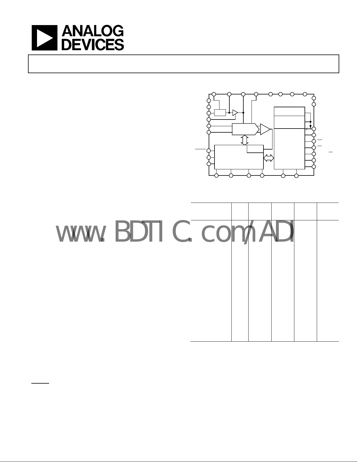
FUNCTIONAL BLOCK DIAGRAM
TEMP
REFBUFIN
AGND
AVDD
PDREF
PDBUF
CNVST
RESET
REF
IN+
IN–
PD
CONTROL L OGIC AND
CALIBRAT ION CI RCUITRY
WARP IMPULSE BIPOLAR TEN
REF REFGND
REF
AMP
SWITCHED
CAP DAC
CLOCK
Figure 1.
EE
AD7634
SERIAL DATA
CONFIGURATI ON
PARALLEL
INTERF ACE
MODE0 MODE1
Table 1. 48-Lead PulSAR Selection
)
500 to
570
(kSPS
AD7650
AD7652
AD7664
AD7666
AD7665
AD7654
AD7655
100 to
250
Res
ts)
(kSPS
Input Type
Bipolar 14 AD7951
Differential
Bipolar
Unipolar
Bipolar 16
Differential
Unipolar
Simultaneous/
Multichannel
Unipolar
Differential
Unipolar
Differential
Bipolar
(Bi
14 AD7952
16
AD7651
AD7660
AD7661
AD7610
AD7663
16 AD7675 AD7676 AD7677
16
18 AD7678 AD7679 AD7674 AD7641
18 AD7631 AD7634
One Technology Way, P.O. Box 9106, Norwood, MA 02062-9106, U.S.A.
Tel: 781.329.4700 www.analog.com
Fax: 781.461.3113 ©2007 Analog Devices, Inc. All rights reserved.
DGNDDVDD
PORT
SERIAL
PORT
)
18
570 to
1000
(kSPS)
AD7653
AD7667
AD7612
AD7671
OVDD
OGND
D[17:0]
BUSY
RD
CS
D0/OB/2C
D1/A0
D2/A1
>1000
(kSPS
AD7621
AD7622
AD7623
AD7643
)
06406-001
Page 2

AD7634
www.BDTIC.com/ADI
TABLE OF CONTENTS
Features.............................................................................................. 1
Applications....................................................................................... 1
General Description......................................................................... 1
Functional Block Diagram ..............................................................1
Revision History ...............................................................................2
Specifications..................................................................................... 3
Timing Specifications ..................................................................5
Absolute Maximum Ratings............................................................ 7
ESD Caution.................................................................................. 7
Pin Configuration and Function Descriptions............................. 8
Typical Performance Characteristics........................................... 12
Terminology .................................................................................... 16
Theory of Operation ......................................................................17
Overview...................................................................................... 17
Converter Operation.................................................................. 17
Modes of Operation................................................................... 17
Transfer Functions......................................................................18
Typical Connection Diagram ...................................................19
Analog Inputs..............................................................................20
Driver Amplifier Choice ........................................................... 21
Voltage Reference Input/Output.............................................. 22
Power Supplies............................................................................ 22
Conversion Control................................................................... 23
Interfaces.......................................................................................... 24
Digital Interface.......................................................................... 24
Parallel Interface......................................................................... 24
Serial Interface............................................................................ 25
Master Serial Interface............................................................... 25
Slave Serial Interface.................................................................. 27
Hardware Configuration........................................................... 29
Software Configuration............................................................. 29
Microprocessor Interfacing....................................................... 30
Application Information................................................................ 31
Layout Guidelines....................................................................... 31
Evaluating Performance ............................................................ 31
Outline Dimensions....................................................................... 32
Ordering Guide .......................................................................... 32
REVISION HISTORY
1/07—Revision 0: Initial Version
Rev. 0 | Page 2 of 32
Page 3

AD7634
www.BDTIC.com/ADI
SPECIFICATIONS
AVDD = DVDD = 5 V; OVDD = 2.7 V to 5.5 V; VCC = 15 V; VEE = −15 V; V
Table 2.
Parameter Conditions/Comments Min Typ Max Unit
RESOLUTION 16 Bits
ANALOG INPUTS
Differential Voltage Range, VIN (V
0 V to 5 V VIN = 10 V p-p −V
0 V to 10 V VIN = 20 V p-p −2 V
±5 V VIN = 20 V p-p −2 V
±10 V VIN = 40 V p-p −4 V
Operating Voltage Range V
0 V to 5 V −0.1 +5.1 V
0 V to 10 V −0.1 +10.1 V
±5 V −5.1 +5.1 V
±10 V −10.1 +10.1 V
Common-Mode Voltage Range V
5 V V
10 V V
Bipolar Ranges −0.1 0
Analog Input CMRR fIN = 100 kHz 75 dB
Input Current VIN = ±5 V, ±10 V @ 670 kSPS 220
Input Impedance
THROUGHPUT SPEED
Complete Cycle In warp mode 1.49 s
Throughput Rate In warp mode 1 670 kSPS
Time Between Conversions In warp mode 1 ms
Complete Cycle In normal mode 1.75 s
Throughput Rate In normal mode 0 570 kSPS
Complete Cycle In impulse mode 2.22 s
Throughput Rate In impulse mode 0 450 kSPS
DC ACCURACY
Integral Linearity Error
2
Integral Linearity Error 670 kSPS throughput ±1.5 LSB
No Missing Codes 18 Bits
Differential Linearity Error
2
Transition Noise 0.75 LSB
Unipolar Zero Error −0.06 + 0.06 %FS
Bipolar Zero Error −0.03 + 0.03 %FS
Zero Error Temperature Drift ±0.5 ppm/°C
Bipolar Full-Scale Error −0.09 +0.09 %FS
Unipolar Full-Scale Error −0.07 +0.07 %FS
Full-Scale Error Temperature Drift ±0.5 ppm/°C
Power Supply Sensitivity AVDD = 5 V ± 5% 3 LSB
AC ACCURACY
Dynamic Range VIN = 0 to 5 V, fIN = 2 kHz, −60 dB 100 101.8 dB
V
Signal-to-Noise Ratio (SNR) VIN = 0 to 5 V, fIN = 2 kHz 98.5 100.5 dB
V
Signal-to-(Noise + Distortion), SINAD fIN = 2 kHz 100 dB
Total Harmonic Distortion fIN = 2 kHz 112 dB
Spurious-Free Dynamic Range fIN = 2 kHz 113 dB
−3 dB Input Bandwidth VIN = 0 V to 5 V 45 MHz
SAMPLING DYNAMICS
Aperture Delay 2 ns
Aperture Jitter 5 ps rms
Transient Response Full-scale step 500 ns
) − (V
IN+
IN+
IN+
See
)
IN−
, V
to AGND
IN−
, V
IN−
Analog Inputs section
600 kSPS throughput −2.5 ±1.5 +2.5 LSB
−1 + 2.5 LSB
= all other input ranges, fIN = 2 kHz, −60 dB 100 102.5 dB
IN
= all other input ranges, fIN = 2 kHz 98.5 101 dB
IN
= 5 V; all specifications T
REF
+V
REF
+2 V
REF
+2 V
REF
+4 V
REF
/2 − 0.1 V
REF
− 0.2 V
REF
to T
MIN
, unless otherwise noted.
MAX
V
REF
REF
REF
REF
/2 V
REF
V
REF
/2 + 0.1 V
REF
+ 0.2 V
REF
+0.1
1
µA
V
V
V
V
3
4
Rev. 0 | Page 3 of 32
Page 4
AD7634
www.BDTIC.com/ADI
Parameter Conditions/Comments Min Typ Max Unit
INTERNAL REFERENCE PDREF = PDBUF = low
Output Voltage REF @ 25°C 4.965 5.000 5.035 V
Temperature Drift −40°C to +85°C ±3 ppm/°C
Line Regulation AVDD = 5 V ± 5% ±15 ppm/V
Long-Term Drift 1000 hours 50 ppm
Turn-On Settling Time C
REFERENCE BUFFER PDREF = high
REFBUFIN Input Voltage Range 2.4 2.5 2.6 V
EXTERNAL REFERENCE PDREF = PDBUF = high
Voltage Range REF 4.75 5 AVDD + 0.1 V
Current Drain 670 kSPS throughput 250 µA
TEMPERATURE PIN
Voltage Output @ 25°C 311 mV
Temperature Sensitivity 1 mV/°C
Output Resistance 4.33 kΩ
DIGITAL INPUTS
Logic Levels
VIL −0.3 +0.6 V
VIH 2.1 OVDD + 0.3 V
IIL −1 +1 µA
IIH −1 +1 µA
DIGITAL OUTPUTS
Data Format Parallel or serial 18-bit
Pipeline Delay
5
VOL I
VOH I
POWER SUPPLIES
Specified Performance
AVDD 4.75
DVDD 4.75 5 5.25 V
OVDD 2.7 5.25 V
VCC 7 15 15.75 V
VEE −15.75 −15 0 V
Operating Current
7, 8
AVDD
With Internal Reference 18.2 mA
With Internal Reference Disabled 16.5 mA
DVDD 7.1 mA
OVDD 0.3 mA
VCC VCC = 15 V, with internal reference buffer 2.9 mA
VCC = 15 V 2 mA
VEE VEE = −15 V 2 mA
Power Dissipation @ 670 kSPS throughput
With Internal Reference PDREF = PDBUF = low 195 225 mW
With Internal Reference Disabled PDREF = PDBUF = high 175 205 mW
In Power-Down Mode9 PD = high 10 µW
TEMPERATURE RANGE
10
Specified Performance T
1
With VIN = unipolar 5 V or unipolar 10 V ranges, the input current is typically 70 A. In all input ranges, the input current scales with throughput. See the Anal og Inpu ts section.
2
Linearity is tested using endpoints, not best fit. All linearity is tested with an external 5 V reference.
3
LSB means least significant bit. All specifications in LSB do not include the error contributed by the reference.
4
All specifications in decibels are referred to a full-scale range input, FSR. Tested with an input signal at 0.5 dB below full-scale, unless otherwise specified.
5
Conversion results are available immediately after completed conversion.
6
4.75 V or V
7
Tested in parallel reading mode.
8
With internal reference, PDREF = PDBUF = low; with internal reference disabled, PDREF = PDBUF = high. With internal reference buffer, PDBUF = low.
9
With all digital inputs forced to OVDD.
10
Consult sales for extended temperature range.
– 0.1 V, whichever is larger.
REF
= 22 µF 10 ms
REF
= 500 µA 0.4 V
SINK
= –500 µA OVDD − 0.6 V
SOURCE
6
5 5.25 V
@ 670 kSPS throughput
to T
MIN
−40 +85 °C
MAX
Rev. 0 | Page 4 of 32
Page 5
AD7634
www.BDTIC.com/ADI
TIMING SPECIFICATIONS
AVDD = DVDD = 5 V; OVDD = 2.7 V to 5.5 V; VCC = 15 V; VEE = −15 V; V
Table 3.
Parameter Symbol Min Typ Max Unit
CONVERSION AND RESET (See Figure 35 and Figure 36)
Convert Pulse Width t1 10 ns
Time Between Conversions t2
Warp Mode/Normal Mode/Impulse Mode1 1.49/1.75/2.22 μs
CNVST Low to BUSY High Delay
BUSY High All Modes (Except Master Serial Read After Convert) t4
Warp Mode/Normal Mode/Impulse Mode
Aperture Delay t5 2 ns
End of Conversion to BUSY Low Delay t6 10 ns
Conversion Time t7
Warp Mode/Normal Mode/Impulse Mode
Acquisition Time, All modes t8 310 ns
RESET Pulse Width t9 10 ns
PARALLEL INTERFACE MODES (See Figure 37 and Figure 39)
CNVST Low to Data Valid Delay
Warp Mode/Normal Mode/Impulse Mode
Data Valid to BUSY Low Delay t11 20 ns
Bus Access Request to Data Valid t12 40 ns
Bus Relinquish Time t13 2 15 ns
MASTER SERIAL INTERFACE MODES2 (See Figure 41 and Figure 42)
CS Low to SYNC Valid Delay
CS Low to Internal SDCLK Valid Delay2
CS Low to SDOUT Delay
CNVST Low to SYNC Delay, Read During Convert
Warp Mode/Normal Mode/Impulse Mode
SYNC Asserted to SDCLK First Edge Delay t18 3 ns
Internal SDCLK Period3 t
Internal SDCLK High3 t
Internal SDCLK Low3 t
SDOUT Valid Setup Time3 t
SDOUT Valid Hold Time3 t
SDCLK Last Edge to SYNC Delay3 t
CS High to SYNC High-Z
CS High to Internal SDCLK High-Z
CS High to SDOUT High-Z
BUSY High in Master Serial Read After Convert3 t
CNVST Low to SYNC Delay Read After Convert
Warp Mode/Normal Mode/Impulse Mode t29
SYNC Deasserted to BUSY Low Delay t30 25 ns
= 5 V; all specifications T
REF
t
35 ns
3
t
10
t
10 ns
14
t
10 ns
15
t
10 ns
16
t
17
30 45 ns
19
15 ns
20
10 ns
21
4 ns
22
5 ns
23
5 ns
24
t
10 ns
25
t
10 ns
26
t
10 ns
27
See Table 4
28
to T
MIN
MAX
50/290/530
, unless otherwise noted.
1.18/1.43/1.68
1.18/1.43/1.68
1.15/1.40/1.65
μs
μs
μs
ns
1.1/1.3/1.5
μs
Rev. 0 | Page 5 of 32
Page 6
AD7634
www.BDTIC.com/ADI
Parameter Symbol Min Typ Max Unit
SLAVE SERIAL/SERIAL CONFIGURATION INTERFACE MODES2
(See Figure 44, Figure 45, and Figure 47)
External SDCLK, SCCLK Setup Time t31 5 ns
External SDCLK Active Edge to SDOUT Delay t32 2 18 ns
SDIN/SCIN Setup Time t33 5 ns
SDIN/SCIN Hold Time t34 5 ns
External SDCLK/SCCLK Period t35 25 ns
External SDCLK/SCCLK High t36 10 ns
External SDCLK/SCCLK Low t37 10 ns
1
In warp mode only, the time between conversions is 1 ms; otherwise, there is no required maximum time.
2
In serial interface modes, the SDSYNC, SDSCLK, and SDOUT timings are defined with a maximum load CL of 10 pF; otherwise, the load is 60 pF maximum.
3
In serial master read during convert mode. See Table 4 for serial master read after convert mode.
Table 4. Serial Clock Timings in Master Read After Convert Mode
DIVSCLK[1] 0 0 1 1
DIVSCLK[0] Symbol 0 1 0 1 Unit
SYNC to SDCLK First Edge Delay Minimum t18 3 20 20 20 ns
Internal SDCLK Period Minimum t19 30 60 120 240 ns
Internal SDCLK Period Maximum t19 45 90 180 360 ns
Internal SDCLK High Minimum t20 15 30 60 120 ns
Internal SDCLK Low Minimum t21 10 25 55 115 ns
SDOUT Valid Setup Time Minimum t22 4 20 20 20 ns
SDOUT Valid Hold Time Minimum t23 5 8 35 90 ns
SDCLK Last Edge to SYNC Delay Minimum t24 5 7 35 90 ns
BUSY High Width Maximum t28
Warp Mode 1.98 2.78
Normal Mode 2.23 3.03
Impulse Mode 2.48 3.28
4.34 7.46
4.59 7.71
4.84 7.96
µs
µs
µs
1.6mA I
TO OUTPUT
PIN
C
L
60pF
500µA I
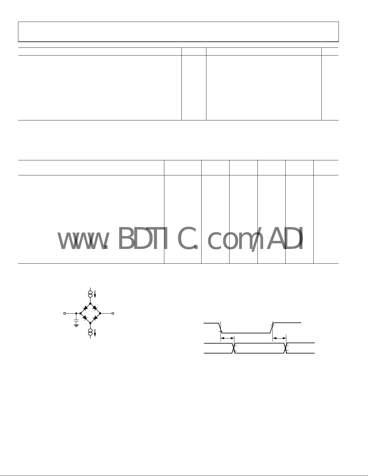
NOTES
1. IN SERIAL INTERFACE MODES, THE SYNC, SDCLK,
AND SDOUT ARE DEFI NED WITH A M AXIMUM LO AD
C
OF 10pF; OTHERWISE, THE LOAD IS 60pF MAXIMUM.
L
Figure 2. Load Circuit for Di
SDOUT, SYNC, and SDCLK Outputs, C
OL
1.4V
OH
gital Interface Timing,
= 10 pF
L
2V
0.8V
t
DELAY
2V
6406-002
Figure 3. Voltage Reference Levels for Timing
t
DELAY
2V
0.8V0.8V
06406-003
Rev. 0 | Page 6 of 32
Page 7
AD7634
www.BDTIC.com/ADI
ABSOLUTE MAXIMUM RATINGS
Table 5.
Parameter Rating
Analog Inputs/Outputs
IN+1, IN−1 to AGND VEE − 0.3 V to VCC + 0.3 V
REF, REFBUFIN, TEMP,
REFGND to AGND
Ground Voltage Differences
AGND, DGND, OGND ±0.3 V
Supply Voltages
AVDD, DVDD, OVDD −0.3 V to +7 V
AVDD to DVDD, AVDD to OVDD ±7 V
DVDD to OVDD ±7 V
VCC to AGND, DGND –0.3 V to +16.5 V
VEE to GND +0.3 V to −16.5 V
Digital Inputs −0.3 V to OVDD + 0 .3 V
PDREF, PDBUF
Internal Power Dissipation2 700 mW
Internal Power Dissipation3 2.5 W
Junction Temperature 125°C
Storage Temperature Range −65°C to +125°C
1
See the Analog Inputs section.
2
Specification is for the device in free air: 48-lead LFQP; θJA = 91°C/W,
θJC = 30°C/W.
3
Specification is for the device in free air: 48-lead LFCSP; θJA = 26°C/W.
AVDD + 0.3 V to
AGND − 0.3 V
±20 mA
Stresses above those listed under Absolute Maximum Ratings
may cause permanent damage to the device. This is a stress
rating only; functional operation of the device at these or any
other conditions above those indicated in the operational
section of this specification is not implied. Exposure to absolute
maximum rating conditions for extended periods may affect
device reliability.
ESD CAUTION
Rev. 0 | Page 7 of 32
Page 8
AD7634
www.BDTIC.com/ADI
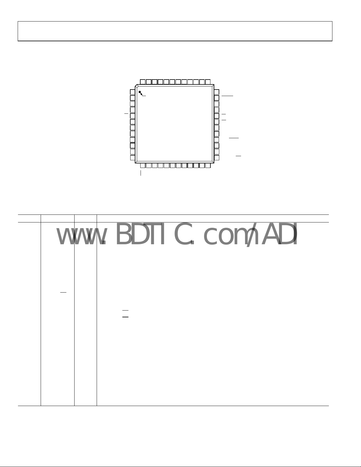
PIN CONFIGURATION AND FUNCTION DESCRIPTIONS
VEE
DGND
IN–
VCC
REFGND
REF
36
BIPOLAR
35
CNVST
34
PD
33
RESET
32
CS
31
RD
30
TEN
29
BUSY
28
D17/SCCS
27
D16/SCCLK
26
D15/SCIN
25
D14/HW/SW
D12/SYNC
D10/SDOUT
D11/SDCLK
D13/RDERROR
06406-004
AGND
AVDD
MODE0
MODE1
D0/OB/2C
WARP
IMPULSE
D1/A0
D2/A1
D3
D4/DIVSCLK[0]
D5/DIVSCLK[1]
PDBUF
PDREF
REFBUFIN
48 47 46 45 44 43 42 41 40 39 38 37
1
PIN 1
2
3
4
5
6
7
8
9
10
11
12
13
14 15 16 17 18 19 20 21 22 23 24
D6/EXT/INT
D8/INVSCLK
D7/INVSYNC
IN+
TEMP
AVDD
AD7634
TOP VIEW
(Not to S cale)
OVDD
OGND
D9/RDC/SDIN
AGND
DVDD
Figure 4. Pin Configuration
Table 6. Pin Function Descriptions
Pin No. Mnemonic Type1 Description
1, 42 AGND P
Analog Power Ground Pins. Ground reference point for all analog I/O. All analog I/O should be referenced to AGND and should be connected to the analog ground plane of the system. In addition, the
AGND, DGND, and OGND voltages should be at the same potential.
2, 44 AVDD P Analog Power Pins. Nominally 4.75 V to 5.25 V and decoupled with 10 μF and 100 nF capacitors.
3, 4 MODE[0:1] DI Data Input/Output Interface Mode Selection.
Interface Mode MODE1 MODE0 Description
0 Low Low 18-bit interface
1 Low High 16-bit interface
2 High Low 8-bit (byte) interface
3 High High Serial interface
2
5
D0/OB/2C
DI/O
In 18-bit parallel mode, this output is used as Bit 0 of the parallel port data output bus and the data
coding is straight binary. In all other modes, this pin allows the choice of straight binary or twos
complement.
When OB/2C = high, the digital output is straight binary
When OB/2C
= low, the MSB is inverted resulting in a twos complement output from its internal shift
register.
6 WARP DI2
Conversion Mode Selection. See the Modes of Operation section for a more detailed description. Used
in conjunction with the IMPULSE input per the following:
Conversion Mode WARP IMPULSE
Normal Low Low
Impulse Low High
Warp High Low
Normal High High
7 IMPULSE DI2
Conversion Mode Selection. See the WARP pin description in this table. See the Modes of Operation
section for a more detailed description.
8 D1/A0 DI/O
When MODE[1:0] = 0, this pin is Bit 1 of the parallel port data output bus. In all other modes, this
input pin controls the form in which data is output as shown in Table 7.
Rev. 0 | Page 8 of 32
Page 9

AD7634
www.BDTIC.com/ADI
Pin No. Mnemonic Type1 Description
9 D2/A1 DI/O
10 D3 DO
11, 12 D[4:5] or DI/O When MODE[1:0] = 0, 1, or 2, these pins are Bit 4 and Bit 5 of the parallel port data output bus.
DIVSCLK[0:1]
13 D6 or DO/I When MODE[1:0] = 0, 1, or 2, this output is used as Bit 6 of the parallel port data output bus.
14 D7 or
INVSYNC
15 D8 or DI/O When MODE[1:0] = 0, 1, or 2, this output is used as Bit 8 of the parallel port data output bus.
INVSCLK
16 D9 or DI/O When MODE[1:0] = 0, 1, or 2, this output is used as Bit 9 of the parallel port data output bus.
RDC or
SDIN
17 OGND P
18 OVDD P
19 DVDD P
20 DGND P
21 D10 or DI/O When MODE[1:0] = 0, 1, or 2, this output is used as Bit 10 of the parallel port data output bus.
SDOUT
22 D11 or DI/O When MODE[1:0] = 0, 1, or 2, this output is used as Bit 11 of the parallel port data output bus.
SDCLK
EXT/INT
DI/O
When MODE[1:0] = 0, this pin is Bit 2 of the parallel port data output bus.
When MODE[1:0] = 1 or 2, this input pin controls the form in which data is output as shown in Table 7.
When MODE[1:0] = 0, 1, or 2, this output is used as Bit 3 of the parallel port data output bus.
This pin is always an output, regardless of the interface mode.
When MODE[1:0] = 3, serial data clock division selection. When using serial master read after convert
mode (EXT/INT = low, RDC/SDIN = low), these inputs can be used to slow down the internally
generated serial clock that clocks the data output. In other serial modes, these pins are high
impedance outputs.
When MODE[1:0] = 3, Serial Data Clock Source Select. In serial mode, this input is used to select
the internally generated (master) or external (slave) serial data clock for the AD7634 output data.
When EXT/INT
When EXT/INT = high (slave mode), the output data is synchronized to an external clock signal (gated by CS)
connected to the SDCLK input.
When MODE[1:0] = 0, 1, or 2, this output is used as Bit 7 of the parallel port data output bus.
When MODE[1:0] = 3, Serial Data Invert Sync Select. In serial master mode (MODE[1:0] = 3,
EXT/INT
When INVSYNC = low, SYNC is active high.
When INVSYNC = high, SYNC is active low.
When MODE[1:0] = 3, Invert SDCLK/SCCLK Select. This input is used to invert both SDCLK and SCCLK.
When INVSCLK = low, the rising edge of SDCLK/SCCLK are used.
When INVSCLK = high, the falling edge of SDCLK/SCCLK are used.
When MODE[1:0] = 3, Serial Data Read During Convert. In serial master mode (MODE[1:0] = 3,
EXT/INT
When RDC = low, the current result is read after conversion. Note the maximum throughput is not
attainable in this mode.
When RDC = high, the previous conversion result is read during the current conversion.
When MODE[1:0] = 3, Serial Data In. In serial slave mode (MODE[1:0] = 3, EXT/INT
used as a data input to daisy-chain the conversion results from two or more ADCs onto a single SDOUT
line. The digital data level on SDIN is output on SDOUT with a delay of 16 SDCLK periods after the initiation
of the read sequence.
Input/Output Interface Digital Power Ground. Ground reference point for digital outputs. Should be
connected to the system digital ground ideally at the same potential as AGND and DGND.
Input/Output Interface Digital Power. Nominally at the same supply as the supply of the host interface
2.5 V, 3 V, or 5 V and decoupled with 10 μF and 100 nF capacitors.
Digital Power. Nominally at 4.75 V to 5.25 V and decoupled with 10 μF and 100 nF capacitors. Can be
supplied from AVDD.
Digital Power Ground. Ground reference point for digital outputs. Should be connected to system
digital ground ideally at the same potential as AGND and OGND.
When MODE[1:0] = 3, Serial Data Output. In all serial modes, this pin is used as the serial data output
synchronized to SDCLK. Conversion results are stored in an on-chip register. The AD7634 provides the
conversion result, MSB first, from its internal shift register. The data format is determined by the logic
level of OB/2C
When EXT/INT
When EXT/INT = high (slave mode):
When INVSCLK = low, SDOUT is updated on SDCLK rising edge.
When INVSCLK = high, SDOUT is updated on SDCLK falling edge.
When MODE[1:0] = 3, Serial Data Clock. In all serial modes, this pin is used as the serial data clock input
or output, dependent on the logic state of the EXT/INT pin. The active edge where the data SDOUT is
updated depends on the logic state of the INVSCLK pin.
= low (master mode), the internal serial data clock is selected on SDCLK output.
= low), this input is used to select the active state of the SYNC signal.
= low), RDC is used to select the read mode. See the Master Serial Interface section.
= high), SDIN can be
.
= low (master mode), SDOUT is valid on both edges of SDCLK.
Rev. 0 | Page 9 of 32
Page 10

AD7634
www.BDTIC.com/ADI
Pin No. Mnemonic Type1 Description
23 D12 or DO When MODE[1:0] = 0, 1, or 2, this output is used as Bit 12 of the parallel port data output bus.
SYNC
24 D13 or DO When MODE[1:0] = 0, 1, or 2, this output is used as Bit 13 of the parallel port data output bus.
RDERROR
25 D14 or DI/O When MODE[1:0] = 0, 1, or 2, this output is used as Bit 14 of the parallel port data output bus.
26 D15 or DI/O When MODE[1:0] = 0, 1, or 2, this output is used as Bit 15 of the parallel port data output bus.
SCIN
27 D16 or DI/O When MODE[1:0] = 0, 1, or 2, this output is used as Bit 16 of the parallel port data output bus.
SCCLK
28 D17 or DI/O When MODE[1:0] = 0, 1, or 2, this output is used as Bit 17 of the parallel port data output bus.
29 BUSY DO
30 TEN DI2 Input Range Select. Used in conjunction with BIPOLAR per the following:
0 V to 5 V Low Low
0 V to 10 V Low High
±5 V High Low
±10 V High High
31
32
33 RESET DI
34 PD DI2
35
36 BIPOLAR DI2 Input Range Select. See description for Pin 30.
HW/SW
SCCS
RD
CS
CNVST
DI
DI
DI
When MODE[1:0] = 3, Serial Data Frame Synchronization. In serial master mode (MODE[1:0] = 3,
EXT/INT
data clock.
When a read sequence is initiated and INVSYNC = low, SYNC is driven high and remains high while the
SDOUT output is valid.
When a read sequence is initiated and INVSYNC = high, SYNC is driven low and remains low while the
SDOUT output is valid.
When MODE[1:0] = 3, Serial Data Read Error. In serial slave mode (MODE[1:0] = 3, EXT/INT
output is used as an incomplete data read error flag. If a data read is started and not completed when
the current conversion is completed, the current data is lost and RDERROR is pulsed high.
When MODE[1:0] = 3, Serial Configuration Hardware/Software Select. In serial mode, this input is used
to configure the AD7634 by hardware or software. See the Hardware Configuration section and
Software Configuration section.
When HW/SW = low, the AD7634 is configured through software using the serial configuration register.
When HW/SW
When MODE[1:0] = 3, Serial Configuration Data Input. In serial software configuration mode (HW/SW
low), this input is used to serially write in, MSB first, the configuration data into the serial configuration
register. The data on this input is latched with SCCLK. See the Software Configuration section.
When MODE[1:0] = 3, Serial Configuration Clock. In serial software configuration mode (HW/SW
this input is used to clock in the data on SCIN. The active edge where the data SCIN is updated
depends on the logic state of the INVSCLK pin. See the Software Configuration section.
When MODE[1:0] = 3, Serial Configuration Chip Select. In serial software configuration mode
(HW/SW
Busy Output. Transitions high when a conversion is started and remains high until the conversion
is completed and the data is latched into the on-chip shift register. The falling edge of BUSY can be
used as a data-ready clock signal. Note that in master read after convert mode (MODE[1:0] = 3,
EXT/INT = low, RDC = low), the busy time changes according to Table 4.
Input Range BIPOLAR TEN
Read Data. When CS and RD are both low, the interface parallel or serial output bus is enabled.
Chip Select. When CS and RD are both low, the interface parallel or serial output bus is enabled. CS is
also used to gate the external clock in slave serial mode (not used for serial configurable port).
Reset Input. When high, reset the AD7634. Current conversion, if any, is aborted. The falling edge of
RESET resets the data outputs to all zeros (with OB/2C
the Digital Interface section. If not used, this pin can be tied to OGND.
Power-Down Input. When PD = high, power down the ADC. Power consumption is reduced and
conversions are inhibited after the current one is completed. The digital interface remains active
during power down.
Conversion Start. A falling edge on CNVST puts the internal sample-and-hold into the hold state and
initiates a conversion.
= low), this output is used as a digital output frame synchronization for use with the internal
= high), this
= high, the AD7634 is configured through dedicated hardware input pins.
= low),
= low), this input enables the serial configuration port. See the Software Configuration section.
= high) and clears the configuration register. See
=
Rev. 0 | Page 10 of 32
Page 11

AD7634
www.BDTIC.com/ADI
Pin No. Mnemonic Type1 Description
37 REF AO/I
38 REFGND AI Reference Input Analog Ground. Connected to analog ground plane.
39 IN− AI
40 VCC P High Voltage Positive Supply. Normally 7 V to 15 V.
41 VEE P High Voltage Negative Supply. Normally 0 V to −15 V (0 V in unipolar ranges).
43 IN+ AI
45 TEMP AO
46 REFBUFIN AI
47 PDREF DI Internal Reference Power-Down Input.
48 PDBUF DI Internal Reference Buffer Power-Down Input.
1
AI = analog input; AI/O = bidirectional analog; AO = analog output; DI = digital input; DI/O = bidirectional digital; DO = digital output; P = power.
2
In serial configuration mode (MODE[1:0] = 3, HW/
Hardware Configuration section and the Software Configuration section.
Reference Input/Output. When PDREF/PDBUF = low, the internal reference and buffer are enabled, producing 5 V on this pin. When PDREF/PDBUF = high, the internal reference and buffer are disabled, allowing
an externally supplied voltage reference up to AVDD volts. Decoupling with at least a 22 μF capacitor is
required with or without the internal reference and buffer. See the Voltage Reference Input/Output
section.
Analog Input. Referenced to IN+.
In the 0 V to 5 V input range, IN− is between 0 V and V
range, IN− is between 0 V and 2 V
V centered about V
REF
In the ±5 V and ±10 V ranges, IN− is true bipolar up to ±2 V
V centered about V
REF
.
REF
V (±5 V range) or ±4 V
REF
/2. In the 0 V to 10 V
REF
V (±10 V range)
REF
and centered about 0 V.
In all ranges, IN− must be driven 180° out of phase with IN+.
Analog Input. Referenced to IN−.
In the 0 V to 5 V input range, IN+ is between 0 V and V
range, IN+ is between 0 V and 2 V
V centered about V
REF
V centered about V
REF
REF
In the ±5 V and ±10 V ranges, IN+ is true bipolar up to ±2 V
.
V (±5 V range) or ±4 V
REF
/2. In the 0 V to 10 V
REF
V (±10 V range)
REF
and centered about 0 V.
In all ranges, IN+ must be driven 180° out of phase with IN−
Temperature Sensor Analog Output. When the internal reference is enabled (PDREF = PDBUF = low),
this pin outputs a voltage proportional to the temperature of the AD7634. See the Voltage Reference
Input/Output section.
Reference Buffer Input. When using an external reference with the internal reference buffer (PDBUF = low,
PDREF = high), applying 2.5 V on this pin produces 5 V on the REF pin. See the Voltage Reference
Input/Output section.
When low, the internal reference is enabled.
When high, the internal reference is powered down, and an external reference must be used.
When low, the buffer is enabled (must be low when using internal reference).
When high, the buffer is powered-down.
SW
= low), this input is programmed with the serial configuration register and this pin is a don’t care. See the
Table 7. Data Bus Interface Definition
MODE MODE1 MODE0 D0/OB/2C D1/A0 D2/A1 D[3] D[4:9] D[10:11] D[12:15] D[16:17] Description
0 0 0 R[0] R[1] R[2] R[3] R[4:9] R[10:11] R[12:15] R[16:17] 18-bit parallel
1 0 1
1 0 1
2 1 0
2 1 0
2 1 0
2 1 0
3 1 1
OB/2C
OB/2C
OB/2C
OB/2C
OB/2C
OB/2C
OB/2C
A0 = 0 R[2] R[3] R[4:9] R[10:11] R[12:15] R[16:17] 16-bit high word
A0 = 1 R[0] R[1] All zeros 16-bit low word
A0 = 0 A1 = 0 All High-Z R[10:11] R[12:15] R[16:17] 8-bit high byte
A0 = 0 A1 = 1 All High-Z R[2:3] R[4:7] R[8:9] 8-bit midbyte
A0 = 1 A1 = 0 All High-Z R[0:1] All zeros 8-bit low byte
A0 = 1 A1 = 1 All High-Z All zeros R[0:1] 8-bit low byte
All High-Z Serial interface Serial interface
Rev. 0 | Page 11 of 32
Page 12

AD7634
www.BDTIC.com/ADI
TYPICAL PERFORMANCE CHARACTERISTICS
AVDD = DVDD = 5 V; OVDD = 5 V; VCC = 15 V; VEE = −15 V; V
2.5
2.0
1.5
1.0
0.5
0
INL (LSB)
–0.5
–1.0
–1.5
–2.0
–2.5
0 262144
65536 131072 196608
Figure 5. Integral Nonlinearity vs. Code, Bipolar 10 V Range
120
100
80
60
40
NUMBER OF UNITS
20
0
–2.0 2.0
–1.2 –0.8 –0.4 0 0.4 0.8 1.2 1. 6–1.6
INL DISTRI BUTION (L SB)
Figure 6. Integral Nonlinearity Distribution, Unipolar 10 V Range
(288 D
70000
60000
POSITIVE INL = 1.40LSB
NEGATIV E INL = –1. 10LSB
CODE
evices)
59925
NEGATIVE INL
POSITIVE INL
σ = 0.80
= 5 V; TA = 25°C.
REF
06406-005
06406-006
2.5
2.0
1.5
1.0
0.5
DNL (LS B)
0
–0.5
–1.0
0 262144
65536 131072 196608
POSITIVE DNL = 1.28LSB
NEGATIVE DNL = –0.63LSB
CODE
Figure 8. Differential Nonlinearity vs. Code, Bipolar 10 V Range
180
160
140
120
100
80
60
NUMBER OF UNITS
40
20
0
–2.0 2.0
Figure 9. Differential Nonlinearity Dist
–1.2 –0.8 –0.4 0 0.4 0.8 1.2 1. 6–1.6
DNL DISTRIBUT ION (LSB)
ribution, Bipolar 5 V Range
NEGATIVE DNL
POSITIVE DNL
(288 Devices)
60000
50000
54874
56811
σ = 0.75
6406-008
06406-009
50000
40000
30000
COUNTS
20000
10000
00
0
1FFFE 20008
20000 20002 20004 20006
32769
1997
25
34164
2172
CODE IN HEX
Figure 7. Histogram of 261,120 Conversions of a DC Input
at the C
ode Center, Bipolar 5 V Range
20
00
06406-007
40000
30000
COUNTS
20000
10000
005
0
Figure 10. Histogram of 261,120 Conversions of a DC Input
the Code Transition, Bipolar 5 V Range
at
Rev. 0 | Page 12 of 32
11838
CODE IN HEX
6901
294349
00
200061FFF C 1FFFE 20000 20002 20004
06406-010
Page 13

AD7634
–
www.BDTIC.com/ADI
0
–20
–40
–60
–80
–100
–120
–140
AMPLITUDE (dB OF FULL SCALE)
–160
–180
0
FREQUENCY (kHz)
200 250 30050 100 150
f
= 670kSPS
S
f
= 20.1kHz
IN
SNR = 98.3dB
THD = –116.8dB
SFDR = 121dB
SINAD = 97.8dB
Figure 11. FFT 20 kHz, Bipolar 5 V Range, Internal Reference
06406-011
103.0
102.5
102.0
101.5
101.0
100.5
SNR, SINAD REFERRED TO FULL SCALE (dB)
100.0
–60 –50 –40 –30 –20 –10 0
INPUT LEVEL (dB)
±5V
0V TO 10V
0V TO 5V
±10V
SNR
SINAD
Figure 14. SNR and SINAD vs. Input Level (Referred to Full Scale)
06406-014
100
98
96
94
ENOB
92
90
88
SNR, SINAD (dB)
86
84
82
80
1 10 100 10 00
SINAD
FREQUENCY (kHz)
SNR
18.0
17.5
17.0
16.5
16.0
15.5
15.0
14.5
14.0
13.5
13.0
Figure 12. SNR, SINAD, and ENOB vs. Frequency, Unipolar 5 V Range
103
102
101
100
SNR (dB)
99
0V TO 10V
0V TO 5V
±10V
±5V
70
SFDR
–80
–90
–100
ENOB (Bits)
06406-012
–110
–120
THD, HARMONICS (dB)
–130
HARMONIC
–140
1 10 100 1000
THD
THIRD
FREQUENCY (kHz)
SECOND
HARMONIC
140
120
100
80
60
40
20
0
SFDR (dB)
06406-015
Figure 15. THD, Harmonics, and SFDR vs. Frequency, Unipolar 5 V Range
103
102
101
100
SINAD (dB)
99
0V TO 10V
0V TO 5V
±10V
±5V
98
97
–55 –35 –15 5 25 45 65 85 105 125
TEMPERATURE ( °C)
Figure 13. SNR vs. Temperature
06406-013
98
97
–55 –35 –15 5 25 45 65 85 105 125
Figure 16. SINAD vs. Temperature
Rev. 0 | Page 13 of 32
TEMPERATURE ( °C)
06406-016
Page 14

AD7634
–
www.BDTIC.com/ADI
100
128
–104
–108
–112
–116
THD (dB)
–120
–124
–128
–55 –35 –15 5 25 45 65 85 105 125
±10V
±5V
0V TO 5V
0V TO 10V
TEMPERATURE ( °C)
Figure 17. THD vs. Temperature
20
16
12
8
4
0
–4
–8
–12
–16
–20
ZERO/OF FSET ERROR, FULL- SCALE ERROR (LS B)
–55 –35 –15 5 25 45 65 85 105 125
ZERO/OFFSET ERROR
NEGATIVE
FULL-SCAL E ERROR
TEMPERATURE (° C)
POSITIVE
FULL-SCAL E ERROR
±5V
0V TO 5V
06406-020
124
120
116
112
SFDR (dB)
108
104
100
–35 –15 5 25 45 65 85 105
–55 125
06406-017
0V TO 10V
±10V
TEMPERATURE ( °C)
Figure 20. SFDR vs. Temperature (Excludes Harmonics)
5.0080
5.0060
5.0040
5.0020
(V)
5.0000
REF
V
4.9980
4.9960
4.9940
4.9920
–55 125
–35–155 25456585105
06406-018
TEMPERATURE (°C)
06406-021
Figure 18. Zero/Offset Error, Positive and Negative Full-Scale Error vs.
Temp
erature, All Normalized to 25°C
60
50
40
30
20
NUMBER OF UNITS
10
0
012345678
REFERENCE DRIFT (ppm/°C)
Figure 19. Reference Voltage Temperature Coef
ficient Distribution (247 Devices)
Figure 21. Typical Reference Voltage Output vs. Temperature (3 Devices)
6406-049
Rev. 0 | Page 14 of 32
100000
10000
1000
100
0.1
OPERATING CURRENTS (µA)
0.01
0.001
10
1
AVDD, WARP/NO RMAL
DVDD, ALL MO DES
AVDD, IMPUL SE
VCC +15V
VEE –15V
ALL MODES
OVDD, ALL MODES
PDREF = PDBUF = HIGH
10 100 1000 10000 100000 1000000
SAMPLING RATE (SPS)
Figure 22. Operating Currents vs. Sample Rate
06406-022
Page 15

AD7634
www.BDTIC.com/ADI
700
PD = PDBUF = PDREF = HIGH
600
500
400
300
200
100
POWER-DOW N OPERATING CURRENTS (nA)
0
–55 105
–35 –15 5 25 45 65 85
TEMPERATURE (° C)
VEE, –15V
VCC, +15V
DVDD
OVDD
AVDD
Figure 23. Power-Down Operating Currents vs. Temperature
06406-023
50
45
40
35
30
25
DELAY (ns)
20
12
t
15
10
5
0
0 50 100 150 200
OVDD = 2.7V @ 25°C
OVDD = 5V @ 25°C
C
L
OVDD = 2.7V @ 85°C
OVDD = 5V @ 85°C
(pF)
Figure 24. Typical Delay vs. Load Capacitance C
6406-024
L
Rev. 0 | Page 15 of 32
Page 16

AD7634
V
www.BDTIC.com/ADI
TERMINOLOGY
Least Significant Bit (LSB)
The least significant bit, or LSB, is the smallest increment that
n be represented by a converter. For a fully differential input
ca
ADC with N bits of resolution, the LSB expressed in volts is
INp-p
VLSB2)( =
N
Integral Nonlinearity Error (INL)
Linearity error refers to the deviation of each individual code
f
rom a line drawn from negative full scale through positive fullscale. The point used as negative full scale occurs a ½ LSB before
the first code transition. Positive full scale is defined as a level
1½ LSBs beyond the last code transition. The deviation is measured from the middle of each code to the true straight line.
Differential Nonlinearity Error (DNL)
In an ideal ADC, code transitions are 1 LSB apart. Differential
onlinearity is the maximum deviation from this ideal value. It
n
is often specified in terms of resolution for which no missing
codes are guaranteed.
Bipolar Zero Error
The difference between the ideal midscale input voltage (0 V)
nd the actual voltage producing the midscale output code.
a
Unipolar Offset Error
The first transition should occur at a level ½ LSB above analog
round. The unipolar offset error is the deviation of the actual
g
transition from that point.
Full-Scale Error
The last transition (from 111…10 to 111…11 in straight binary
for
mat) should occur for an analog voltage 1½ LSB below the
nominal full-scale. The full-scale error is the deviation in LSB
(or % of full-scale range) of the actual level of the last transition
from the ideal level and includes the effect of the offset error.
Closely related is the gain error (also in LSB or % of full-scale
range), which does not include the effects of the offset error.
Dynamic Range
Dynamic range is the ratio of the rms value of the full scale to
t
he rms noise measured for an input typically at −60 dB. The
value for dynamic range is expressed in decibels.
Signal-to-Noise Ratio (SNR)
SNR is the ratio of the rms value of the actual input signal to
t
he rms sum of all other spectral components below the Nyquist
frequency, excluding harmonics and dc. The value for SNR is
expressed in decibels.
Total Harmonic Distortion (THD)
THD is the ratio of the rms sum of the first five harmonic
mponents to the rms value of a full-scale input signal and
co
is expressed in decibels.
Signal-to-(Noise + Distortion) Ratio (SINAD)
SINAD is the ratio of the rms value of the actual input signal to
t
he rms sum of all other spectral components below the Nyquist
frequency, including harmonics but excluding dc. The value for
SINAD is expressed in decibels.
Spurious-Free Dynamic Range (SFDR)
The difference, in decibels (dB), between the rms amplitude of
e input signal and the peak spurious signal.
th
Effective Number of Bits (ENOB)
ENOB is a measurement of the resolution with a sine wave
put. It is related to SINAD and is expressed in bits by
in
ENOB = [(SINA
− 1.76)/6.02]
D
dB
Aperture Delay
Aperture delay is a measure of the acquisition performance
m
easured from the falling edge of the
CNVST
input to when
the input signal is held for a conversion.
Transi ent Res p ons e
The time required for the AD7634 to achieve its rated accuracy
a
fter a full-scale step function is applied to its input.
Reference Voltage Temperature Coefficient
Reference voltage temperature coefficient is derived from the
ypical shift of output voltage at 25°C on a sample of parts at
t
the maximum and minimum reference output voltage (V
measured at T
MIN
REF
, T(25°C), and T
)(TCV
Cppm/ ×
=°
REF
. It is expressed in ppm/°C as
MAX
((
REFREF
×°
C25
MAX
MIN
)MinV–)MaxV
)T–T()(V
10
)
REF
6
where:
V
(Max) = maximum V
REF
V
(Min) = minimum V
REF
(25°C) = V
V
REF
T
MAX
T
MIN
= +85°C.
= –40°C.
REF
at 25°C.
REF
REF
at T
at T
MIN
MIN
, T(25°C), or T
, T(25°C), or T
MAX
MAX
.
.
Rev. 0 | Page 16 of 32
Page 17

AD7634
www.BDTIC.com/ADI
THEORY OF OPERATION
IN+
MSB
131,072C
REF
REFGND
131,072C
IN–
OVERVIEW
The AD7634 is a very fast, low power, precise, 18-bit ADC using
successive approximation capacitive digital-to-analog (CDAC)
architecture.
The AD7634 can be configured at any time for one of four input
anges and conversion mode with inputs in parallel and serial
r
hardware modes or by a dedicated write-only, SPI-compatible
interface via a configuration register in serial software mode.
The AD7634 uses Analog Devices’ patented iCMOS high voltage process to accommodate 0 V to +5 V (10 V p-p), 0 V to
+10 V (20 V p-p), ±5 V (20 V p-p), and ±10 V (40 V p-p) input
ranges on the fully differential IN+ and IN− inputs without the
use of conventional thin films. Only one acquisition cycle, t
required for the inputs to latch to the correct configuration. Resetting or power cycling is not required for reconfiguring the ADC.
The AD7634 features different modes to optimize performance
rding to the applications. It is capable of converting 670,000
acco
samples per second (670 kSPS) in warp mode, 570 kSPS in normal
mode, and 450 kSPS in impulse mode.
The AD7634 provides the user with an on-chip, track-and-hold,
s
uccessive approximation ADC that does not exhibit any pipeline or latency, making it ideal for multiple, multiplexed channel
applications.
For unipolar input ranges, the AD7634 typically requires three
pplies: VCC, AVDD (which can supply DVDD), and OVDD
su
(which can be interfaced to either 5 V, 3.3 V, or 2.5 V digital logic).
For bipolar input ranges, the AD7634 requires the use of the
additional VEE supply.
The device is housed in a Pb-fr
tiny LFCSP (7 mm × 7 mm) that combine space savings with
flexibility. In addition, the AD7634 can be configured as either
a parallel or serial SPI-compatible interface.
ee, 48-lead LQFP or a 48-lead
65,536C 4C 2C C C
65,536C
MSB
4C 2C C C
Figure 25. ADC Simplified Schematic
, is
8
AGND
SWITCHES
COMP
CONTROL
CONTROL
LOGIC
CNVST
BUSY
OUTPUT
CODE
06406-025
LSB
LSB
SW+
SW–
AGND
CONVERTER OPERATION
The AD7634 is a successive approximation ADC based on a
charge redistribution DAC. Figure 25 shows the simplified
chematic of the ADC. The CDAC consists of two identical
s
arrays of 18 binary weighted capacitors, which are connected
to the two comparator inputs.
During the acquisition phase, terminals of the array tied to the
co
mparator’s input are connected to AGND via SW+ and SW−.
All independent switches are connected to the analog inputs. Thus,
the capacitor arrays are used as sampling capacitors and acquire
the analog signal on IN+ and IN− inputs. A conversion phase is
initiated once the acquisition phase is completed and the
CNVST
input goes low. When the conversion phase begins, SW+ and SW−
are opened first. The two capacitor arrays are then disconnected
from the inputs and connected to the REFGND input. Therefore,
the differential voltage between the inputs (IN+ and IN−) captured
at the end of the acquisition phase is applied to the comparator
inputs, causing the comparator to become unbalanced. By switching each element of the capacitor array between REFGND and
REF, the comparator input varies by binary weighted voltage
steps (V
REF
/2, V
/4 through V
REF
/ 262,144). The control logic
REF
toggles these switches, starting with the MSB first, to bring the
comparator back into a balanced condition.
After the completion of this process, the control logic generates
t
he ADC output code and brings the BUSY output low.
MODES OF OPERATION
The AD7634 features three modes of operation: warp, normal,
and impulse. Each of these modes is more suitable to specific
applications. The mode is configured with the input pins, WARP
and IMPULSE, or via the configuration register. See
e pin details; see the Hardware Configuration section and the
th
Software Configuration section for programming the mode
s
election with either pins or configuration register. Note that
when using the configuration register, the WARP and IMPULSE
inputs are don’t cares and should be tied to either high or low.
Table 6 for
Rev. 0 | Page 17 of 32
Page 18

AD7634
www.BDTIC.com/ADI
Warp Mode
Setting WARP = high and IMPULSE = low allows the fastest
nversion rate of up to 670 kSPS. However, in this mode, the
co
full-specified accuracy is guaranteed only when the time between
conversions does not exceed 1 ms. If the time between two
consecutive conversions is longer than 1 ms (after power-up),
the first conversion result should be ignored because in warp mode,
the ADC performs a background calibration during the SAR
conversion process. This calibration can drift if the time between
conversions exceeds 1 ms thus causing the first conversion to
appear offset. This mode makes the AD7634 ideal for applications
where both high accuracy and fast sample rate are required.
Normal Mode
Setting WARP = IMPULSE = low or WARP = IMPULSE = high
allows the fastest mode (570 kSPS) without any limitation on
time between conversions. This mode makes the AD7634 ideal
for asynchronous applications such as data acquisition systems,
where both high accuracy and fast sample rate are required.
Impulse Mode
Setting WARP = low and IMPULSE = high uses the lowest power
dissipation mode and allows power savings between conversions. The maximum throughput in this mode is 450 kSPS, and
in this mode, the ADC powers down circuits after conversion,
making the AD7634 ideal for battery-powered applications.
TRANSFER FUNCTIONS
Except in 18-bit parallel interface mode, using the D0/OB/2C
digital input or via the configuration register, the AD7634 offers
two output codings: straight binary and twos complement. See
Figure 26 and Tabl e 8 for the ideal transfer characteristic and
dig
ital output codes for the different analog input ranges, V
Note that when using the configuration register, the D0/OB/
input is a don’t care and should be tied to either high or low.
111... 111
111... 110
111... 101
ADC CODE (Straight Binary)
000... 010
000... 001
000... 000
–FSR
–FSR + 0.5 LSB
ANALOG INPUT
Figure 26. ADC Ideal Transfer Function
+FSR – 1.5 LSB
+FSR –1LSB–FSR + 1 LSB
.
IN
2C
06406-026
Table 8. Output Codes and Ideal Input Voltages
Description
VIN = 0 V to +5 V
(10 V p-p)
VIN = 0 V to +10 V
(20 V p-p)
FSR − 1 LSB +4.999962 V +9.999924 V +9.999924 V +19.999847 V 0x3FFFF
V
= 5 V Digital Output Code
REF
VIN = ±5 V
(20 V p-p)
VIN = ±10 V
(40 V p-p)
Straight Binary Twos Complement
1
0x1FFFF
FSR − 2 LSB +4.999924 V +9.999847 V +9.999847 V +19.999695 V 0x3FFFE 0x1FFFE
Midscale + 1 LSB +38.15 µV −76.29 µV −76.29 µV +152.59 µV 0x20001 0x00001
Midscale 0 V 0 V 0 V 0 V 0x20000 0x00000
Midscale − 1 LSB −38.15 µV −76.29 µV −76.29 µV −152.59 µV 0x1FFFF 0x3FFFF
−FSR + 1 LSB −4.999962 V −9.999924 V −9.999924 V −19.999847 V 0x00001 0x20001
−FSR −5 V −10 V −10 V −20 V 0x00000
1
This is also the code for overrange analog input.
2
This is also the code for underrange analog input.
2
0x20000
1
2
Rev. 0 | Page 18 of 32
Page 19

AD7634
www.BDTIC.com/ADI
TYPICAL CONNECTION DIAGRAM
Figure 27 shows a typical connection diagram for the AD7634 using the internal reference, serial data interface, and serial configuration
port. Different circuitry from that shown in Figure 27 is optional and is discussed in the following sections.
DIGIT AL
SUPPLY (5V)
100nF 100nF
AD7634
D0/OB/2C
MODE[1:0]
BIPOLAR
NOTE 3
PDBUF
IMPULSE
RD CS
BUSY
SDCLK
SDOUT
SCCLK
SCIN
SCCS
CNVST
HW/SW
TEN
WARP
RESETPD
10µF
DIGIT AL
INTERF ACE
SUPPLY
(2.5V, 3.3V, OR 5V)
NOTE 7
33Ω
OVDD
D
CLOCK
MicroConverter®/
MICROP ROCESSO R/
DSP
SERIAL
PORT 1
SERIAL
PORT 2
SUPPLY (5V)
+7V TO +15.75V
SUPPLY
–7V TO –15.75V
SUPPLY
NOTE 6
ANALOG
INPUT+
ANALOG
INPUT–
ANALOG
10µF
10µF
NOTE 4
NOTE 2
U1
C
C
NOTE 2
U1
10µF 100nF
100nF
100nF
C
REF
22µF
100nF
15Ω
2.7nF
15Ω
NOTE 5
10Ω
10µF
AVDD
AGND DGND DVDD OVDD OGND
VCC
VEE
NOTE 3
REF
REFBUFIN
REFGND
IN+
IN–
PDREF
C
2.7nF
C
NOTE 1
NOTES
1. ANALOG INPUT S ARE DIF FERENT IAL (ANT IPHASE) . SEE ANAL OG I NPUTS SE CTION.
2. THE AD8021 IS RECOM MENDED. SEE DRIVE R AMPLI FIER CHO ICE SECTION.
3. THE CONFIGURATI ON SHOWN IS USING THE INTERNAL REFERENCE. SEE VOLTAGE REFERENCE I NPUT/OUTPUT SECT ION.
4. A 22µF CE RAMIC CAPACI TOR ( X5R, 1206 SI ZE) IS RECOMME NDED (FO R EXAMPL E, PANAS ONIC ECJ4Y B1A226M).
SEE VOL TAGE RE FERENCE I NPUT/ OUTPUT SECTIO N.
5. OPTIONAL, SEE POWER SUPPLIES SECTION.
6. THE VCC AND VEE SUPP LIES SHOULD BE V CC = [VIN( MAX) + 2V] AND VEE = [ VIN(MI N) – 2V] FO R BIPO LAR INPUT RANGES.
FOR UNIPOLAR INPUT RANGES, VEE CAN BE 0V. SEE POWER SUPPLIES SECTION.
7. OPTIONAL LOW JI TTER CNVST, SEE CONVERSION CONTROL SECTION.
8. A SEPARATE ANALOG AND DIGITAL GRO UND PLANE I S RECOM MENDED, CO NNECTED TOGETHER DIRECT LY UNDER THE ADC.
SEE LAYOUT GUIDELINES SECTION.
AGND
DGND
NOTE 8
Figure 27. Typical Connection Diagram Shown with Serial Interface and Serial Programmable Port
06406-027
Rev. 0 | Page 19 of 32
Page 20

AD7634
–
www.BDTIC.com/ADI
ANALOG INPUTS
Input Range Selection
In parallel mode and serial hardware mode, the input range is
selected by using the BIPOLAR (bipolar) and TEN (10 V range)
inputs. See Table 6 for pin details; see the Hardware Configuration
section and the Software Configuration section for programming the mode selection with either pins or configuration
register. Note that when using the configuration register, the
BIPOLAR and TEN inputs are don’t cares and should be tied
to either high or low.
Input Structure
Figure 28 shows an equivalent circuit for the input structure of
the AD7634.
VCC
IN+ OR IN–
C
PIN
VEE
Figure 28. AD7634 Simplified Analog Input
The four diodes, D1 to D4, provide ESD protection for the analog
inputs, IN+ and IN−. Care must be taken to ensure that the analog
input signal never exceeds the supply rails by more than 0.3 V,
because this causes the diodes to become forward-biased and
to start conducting current. These diodes can handle a forwardbiased current of 120 mA maximum. For instance, these conditions
could eventually occur when the input buffer’s U1 supplies are
different from AVDD, VCC, and VEE. In such a case, an input
buffer with a short-circuit current limitation can be used to protect
the part although most op amps’ short-circuit current is <100 mA.
Note that D3 and D4 are only used in the 0 V to 5 V range to
allow for additional protection in applications that are switching
from the higher voltage ranges.
This analog input structure of the AD7634 is a true differential
structure allowing the sampling of the differential signal between
IN+ and IN−. By using this differential input, small signals
common to both inputs are rejected as shown in Figure 29,
which represents the typical CMRR over frequency.
D1
D2
0VTO 5V
RANGE ONLY
AVD D
D3
D4
R
IN
AGND
C
IN
6406-028
120
100
0V TO 5V
80
60
CMRR (dB)
40
20
0
1 10000
Figure 29. Analog Input CMRR vs. Frequency
0V TO 10V
±10V
10 100 1000
FREQUENCY (kHz)
±5V
06406-029
During the acquisition phase for ac signals, the impedance of
the analog inputs, IN+ and IN−, can be modeled as a parallel
combination of Capacitor C
the series connection of R
capacitance. R
is typically 70 Ω and is a lumped component
IN
and the network formed by
PIN
and CIN. C
IN
is primarily the pin
PIN
comprised of serial resistors and the on resistance of the switches.
C
is primarily the ADC sampling capacitor and depending on
IN
the input range selected is typically 48 pF in the 0 V to 5 V range,
typically 24 pF in the 0 V to 10 V and ±5 V ranges, and typically
12 pF in the ±10 V range. During the conversion phase, when the
switches are opened, the input impedance is limited to C
PIN
.
Because the input impedance of the AD7634 is very high, it
can be directly driven by a low impedance source without gain
error. To further improve the noise filtering achieved by the
AD7634 analog input circuit, an external, one-pole RC filter
between the amplifier’s outputs and the ADC analog inputs can
be used, as shown in Figure 27. However, large source impedances significantly affect the ac performance, especially the
THD. The maximum source impedance depends on the amount
of THD that can be tolerated. The THD degrades as a function of
the source impedance and the maximum input frequency, as
shown in Figure 30.
70
–90
200Ω
100Ω
THD (dB)
–110
–130
0
Figure 30. THD vs. Analog Input Frequency and Source Resistance
Rev. 0 | Page 20 of 32
33Ω
15Ω
25 50 75 100
FREQUENCY (kHz)
06406-050
Page 21

AD7634
V
www.BDTIC.com/ADI
DRIVER AMPLIFIER CHOICE
Although the AD7634 is easy to drive, the driver amplifier must
meet the following requirements:
• For multichannel, multiplexed applications, the driver ampli-
fier and the AD7634 analog input circuit must be able to
settle for a full-scale step of the capacitor array at a 18-bit
level (0.0004%). For the amplifier, settling at 0.1% to 0.01%
is more commonly specified. This differs significantly from
the settling time at a 18-bit level and should be verified
prior to driver selection. The AD8021 op amp combines ultralow noise and high gain bandwidth and meets this settling
time requirement even when used with gains of up to 13.
• The noise generated by the driver amplifier needs to be
kept as low as possible to preserve the SNR and transition
noise performance of the AD7634. The noise coming from
the driver is filtered by the external 1-pole low-pass filter,
as shown in Figure 27. The SNR degradation due to the
amplifier is
⎛
⎜
LOSS
=
log20
⎜
⎜
⎜
⎝
NADC
2
+
SNR
⎜
where:
is the noise of the ADC, which is:
V
NADC
2
INp-p
10
SNR
22
20
V =
NADC
f
is the cutoff frequency of the input filter (3.9 MHz).
–3dB
N is the noise factor of the amplifier (+1 in buffer
configuration).
e
and eN− are the equivalent input voltage noise densities
N+
of the op amps connected to IN+ and IN−, in nV/√Hz.
This approximation can be utilized when the resistances
used around the amplifiers are small. If larger resistances are
used, their noise contributions should also be root-sum
squared.
• The driver needs to have a THD performance suitable to
that of the AD7634. Figure 15 shows the THD vs. frequency
that the driver should exceed.
The AD8021 meets these requirements and is appropriate for
almost all applications. The AD8021 needs a 10 pF external
compensation capacitor that should have good linearity as an
NPO ceramic or mica type. Moreover, the use of a noninverting
+1 gain arrangement is recommended and helps to obtain the
best signal-to-noise ratio.
The AD8022 can also be used when a dual version is needed
and a gain of 1 is present. The AD829 is an alternative in applications where high frequency (above 100 kHz) performance is not
required. In applications with a gain of 1, an 82 pF compensation
V
NADC
π
−
3
dB
2
π
2
+
)(
+
N
NefNefV
−
3
dB
2
2
)(
−
N
capacitor is required. The AD8610 is an option when low bias
current is needed in low frequency applications.
Because the AD7634 uses a large geometry, high voltage input
switch, the best linearity performance is obtained when using
the amplifier at its maximum full power bandwidth. Gaining
the amplifier to make use of the more dynamic range of the
ADC results in increased linearity errors. For applications
requiring more resolution, the use of an additional amplifier
with gain should precede a unity follower driving the AD7634.
See Table 9 for a list of recommended op amps.
Table 9. Recommended Driver Amplifiers
Amplifier Typical Application
AD829 ±15 V supplies, very low noise, low frequency
AD8021 ±12 V supplies, very low noise, high frequency
AD8022
±12 V supplies, very low noise, high
frequency, dual
ADA4922-1
±12 V supplies, low noise, high frequency,
single-ended-to-differential driver
AD8610/
⎞
AD8620
⎟
⎟
Single-to-Differential Driver
⎟
⎟
For single-ended sources, a single-to-differential driver, such
⎟
⎠
as the ADA4922-1, can be used because the AD7634 needs to
±13 V supplies, low bias current, low
frequency, single/dual
be driven differentially. The 1-pole filter using R = 15 Ω and
C = 2.7 nF provides a corner frequency of 3.9 MHz.
15Ω
OUT+
OUT–
2.7nF
15Ω
2.7nF
R
R
F
ADA4922-1
REF
G
U2
R1
R2
100nF
ANALOG
IN
INPUT
Figure 31. Single-to-Differential Driver Using the ADA4922-1
VCC
VEE
For unipolar 5 V and 10 V input ranges, the internal (or
external) reference source can be used to level shift U2 for
the correct input span. If using an external reference, the
values for R1/R2 can be lowered to reduce resistive Johnson
noise (1.29E − 10 × √R). For the bipolar ±5 V and ±10 V input
ranges, the reference connection is not required because the
common-mode voltage is 0 V. See Table 10 for R1/R2 for the
different input ranges.
Table 10. R1/R2 Configuration
Input Range R1 R2 Common-Mode Voltage
5 V 2.5 kΩ 2.5 kΩ 2.5 V
10 V 2.5 kΩ Open 5 V
±5 V, ±10 V 100 Ω 0 V
IN+
AD7634
IN–
10µF
REF
06406-052
Rev. 0 | Page 21 of 32
Page 22

AD7634
www.BDTIC.com/ADI
This circuit can also be made discretely, and thus more flexible,
using any of the recommended low noise amplifiers in Tabl e 9.
gain, to preserve the SNR of the converter, the resistors, R
A
and R
, should be kept low.
G
F
VOLTAGE REFERENCE INPUT/OUTPUT
The AD7634 allows the choice of either a very low temperature
drift internal voltage reference, an external reference, or an
external buffered reference.
The internal reference of the AD7634 provides excellent performa
nce and can be used in almost all applications. However, the
linearity performance is guaranteed only with an external reference.
Internal Reference (REF = 5 V) (PDREF = Low, PDBUF = Low)
To use the internal reference, the PDREF and PDBUF inputs
must be low. This enables the on-chip, band gap reference, buffer,
and TEMP sensor, resulting in a 5.00 V reference on the REF pin.
The internal reference is temperature-compensated to 5.000 V
± 35 mV
3 ppm/°C. This typical drift characteristic is shown in
External 2.5 V Reference and Internal Buffer (REF = 5 V) (PDREF = High, PDBUF = Low)
To use an external reference with the internal buffer, PDREF
should be high and PDBUF should be low. This powers down
the internal reference and allows the 2.5 V reference to be applied
to REFBUFIN producing 5 V on the REF pin. The internal reference buffer is useful in multiconverter applications because
a buffer is typically required in these applications to avoid
reference coupling amongst the different converters.
External 5 V Reference (PDREF = High, PDBUF = High)
To use an external reference directly on the REF pin, PDREF
and PDBUF should both be high. PDREF and PDBUF power
down the internal reference and the internal reference buffer,
respectively. For improved drift performance, an external reference, such as the
Reference Decoupling
Whether using an internal or external reference, the AD7634
voltage reference input (REF) has a dynamic input impedance;
therefore, it should be driven by a low impedance source with
efficient decoupling between the REF and REFGND inputs. This
decoupling depends on the choice of the voltage reference but
usually consists of a low ESR capacitor connected to REF and
REFGND with minimum parasitic inductance. A 22 µF (X5R,
1206 size) ceramic chip capacitor (or 47 µF low ESR tantalum
capacitor) is appropriate when using either the internal reference or the
The placement of the reference decoupling is also important to
t
be mounted on the same side as the ADC right at the REF pin
with a thick PCB trace. The REFGND should also connect to
. The reference is trimmed to provide a typical drift of
Figure 19.
ADR445 or ADR435, is recommended.
ADR445/ADR435 external reference.
he performance of the AD7634. The decoupling capacitor should
the reference decoupling capacitor with the shortest distance
and to the analog ground plane with several vias.
For applications that use multiple AD7634 or other PulSAR
vices, it is more effective to use the internal reference buffer
de
to buffer the external 2.5 V reference voltage.
The voltage reference temperature coefficient (TC) directly
pacts full scale; therefore, in applications where full-scale
im
accuracy matters, care must be taken with the TC. For instance,
a ±4 ppm/°C TC of the reference changes full scale by ±1 LSB/°C.
Temperature Sensor
The TEMP pin measures the temperature of the AD7634. To
improve the calibration accuracy over the temperature range, the
output of the TEMP pin is applied to one of the inputs of the
analog switch (such as ADG779), and the ADC itself is used to
m
easure its own temperature. This configuration is shown
in
Figure 32.
ANALOG INPUT
ADG779
C
C
Figure 32. Use of the Temperature Sensor
IN+
TEMP
AD7634
TEMPERATURE
SENSOR
06406-030
POWER SUPPLIES
The AD7634 uses five sets of power supply pins:
VDD: analog 5 V core supply
• A
• V
CC: analog high voltage positive supply
• V
EE: high voltage negative supply
• D
VDD: digital 5 V core supply
• O
VDD: digital input/output interface supply
Core Supplies
The AVDD and DVDD supply the AD7634 analog and digital
cores, respectively. Sufficient decoupling of these supplies is
required consisting of at least a 10 F capacitor and a 100 nF
capacitor on each supply. The 100 nF capacitors should be
placed as close as possible to the AD7634. To reduce the number
of supplies needed, the DVDD can be supplied through a simple
RC filter from the analog supply, as shown in
High Voltage Supplies
The high voltage bipolar supplies, VCC and VEE, are required
and must be at least 2 V larger than the maximum input voltage.
For example, if using the ±10 V range, the supplies should be
±12 V minimum. This allows for 40 V p-p fully differential
input (±10 V on each input IN+ and IN−). Sufficient decoupling of these supplies is also required consisting of at least a
10 F capacitor and a 100 nF capacitor on each supply. For
unipolar operation, the VEE supply can be grounded with
some slight THD performance degradation.
Figure 27.
Rev. 0 | Page 22 of 32
Page 23

AD7634
www.BDTIC.com/ADI
Digital Output Supply
The OVDD supplies the digital outputs and allows direct interface
with any logic working between 2.3 V and 5.25 V. OVDD should
be set to the same level as the system interface. Sufficient decoupling is required consisting of at least a 10 F capacitor and a 100 nF
capacitor with the 100 nF capacitor placed as close as possible
to the AD7634.
Power Sequencing
The AD7634 is independent of power supply sequencing and is
very insensitive to power supply variations on AVDD over a wide
frequency range, as shown in Figure 33.
75
70
65
60
55
50
PSRR (dB)
45
40
35
30
1 10 100 1000 10000
FREQUENCY (kHz)
Figure 33. AVDD PSRR vs. Frequency
6406-051
Power Dissipation vs. Throughput
In impulse mode, the AD7634 automatically reduces its power
consumption at the end of each conversion phase. During the
acquisition phase, the operating currents are very low, which allows
a significant power savings when the conversion rate is reduced
(see
Figure 34). This feature makes the AD7634 ideal for very
ow power, battery-operated applications.
l
It should be noted that the digital interface remains active even
d
uring the acquisition phase. To reduce the operating digital supply
currents even further, drive the digital inputs close to the power
rails, that is, OVDD and OGND.
1000
PDREF = PDBUF = HI GH
WARP MODE POW ER
100
Power Down
Setting PD = high powers down the AD7634, thus reducing
supply currents to their minimums, as shown in Figure 23.
W
hen the ADC is in power down, the current conversion
(if any) is completed and the digital bus remains active. To
further reduce the digital supply currents, drive the inputs to
OVDD or OGND.
Power down can also be programmed with the configuration
egister. See the Software Configuration section for details. Note
r
t
hat when using the configuration register, the PD input is a don’t
care and should be tied to either high or low.
CONVERSION CONTROL
The AD7634 is controlled by the
on
CNVST
is all that is necessary to initiate a conversion. A
detailed timing diagram of the conversion process is shown in
Figure 35. Once initiated, it cannot be restarted or aborted, even
y the power-down input, PD, until the conversion is complete.
b
CNVST
The
signal operates independently of CS and RD
signals.
t
1
CNVST
BUSY
MODE
Although
t
3
t
5
CNVST
t
4
CONVERT ACQUIREACQUI RE CONVERT
t
7
Figure 35. Basic Conversion Timing
is a digital signal, it should be designed with
special care with fast, clean edges and levels with minimum
overshoot, undershoot, or ringing.
CNVST
The
trace should be shielded with ground and a low value
(such as 50 Ω) serial resistor termination should be added close
to the output of the component that drives this line.
For applications where SNR is critical, the
have very low jitter. This can be achieved by using a dedicated
oscillator for
CNVST
generation, or by clocking
high frequency, low jitter clock, as shown in Figure 27.
CNVST
t
2
t
6
input. A falling edge
t
8
CNVST
signal should
CNVST
with a
6406-033
IMPULSE MODE POWER
10
POWER DISSIPATION (mW)
1
1 1000000100000
Figure 34. Power Dissipati
10010 100001000
SAMPLING RATE (kSPS)
on vs. Sample Rate
06406-048
Rev. 0 | Page 23 of 32
Page 24

AD7634
www.BDTIC.com/ADI
INTERFACES
DIGITAL INTERFACE
The AD7634 has a versatile digital interface that can be set up as
either a serial or a parallel interface with the host system. The
serial interface is multiplexed on the parallel data bus. The AD7634
digital interface also accommodates 2.5 V, 3.3 V, or 5 V logic. In
most applications, the OVDD supply pin is connected to the host
system interface 2.5 V to 5.25 V digital supply. Finally, by using the
D0/OB/
coding can be used, except for in a 18-bit parallel interface.
Two signals,
one of these signals is high, the interface outputs are in high
impedance. Usually,
in multicircuit applications and is held low in a single AD7634
design.
the data bus.
RESET
The RESET input is used to reset the AD7634. A rising edge on
RESET aborts the current conversion (if any) and tristates the
data bus. The falling edge of RESET resets the AD7634 and clears
the data bus and configuration register. See
RES
2C
input pin, both twos complement or straight binary
CS
and RD, control the interface. When at least
CS
allows the selection of each AD7634
RD
is generally used to enable the conversion result on
Figure 36 for the
ET timing details.
CS = RD = 0
CNVST
BUSY
t
DATA
BUS
Figure 37. Master Parallel Data Timing for Reading (Continuous Read)
t
1
t
10
t
3
PREVIOUS CONVERSION DATA NEW DATA
4
t
11
Slave Parallel Interface
In slave parallel reading mode, the data can be read either after
each conversion, which is during the next acquisition phase, or
during the following conversion, as shown in Figure 38 and
Figure 39, respectively. When the data is read during the convers
ion, it is recommended that it is read-only during the first half
of the conversion phase. This avoids any potential feedthrough
between voltage transients on the digital interface and the most
critical analog conversion circuitry.
CS
06406-035
t
9
RESET
BUSY
DATA
BUS
t
8
CNVST
Figure 36. RESET Timing
PARALLEL INTERFACE
The AD7634 is configured to use the parallel interface when
the MODE[1:0] pins = 0, 1 or 2 for 18-/16-/8-bit interfaces,
respectively, as detailed in Ta ble 7.
Master Parallel Interface
Data can be continuously read by tying CS and RD low, thus
requiring minimal microprocessor connections. However, in
this mode, the data bus is always driven and cannot be used in
shared bus applications (unless the device is held in RESET).
Figure 37 details the timing for this mode.
RD
BUSY
DATA
BUS
t
6406-034
Figure 38. Slave Parallel Data Timing for Reading (Read After Convert)
CS = 0
CNVST,
RD
BUSY
DATA
BUS
Figure 39. Slave Parallel Data Timing for Reading (Read During Convert)
12
t
3
t
12
CURRENT
CONVERS ION
t
1
PREVIOUS
CONVERSION
t
13
t
4
t
13
06406-036
06406-037
Rev. 0 | Page 24 of 32
Page 25

AD7634
www.BDTIC.com/ADI
18-Bit Interface (Master or Slave)
The 18-bit interface is selected by setting MODE[1:0] = 0. In
this mode, the data output is straight binary.
16-Bit and 8-Bit Interface (Master or Slave)
In the 16-bit (MODE[1:0] = 1) and 8-bit (MODE[1:0] = 2)
interfaces, Pin A0 and Pin A1 allow a glueless interface to a
16- or 8-bit bus, as shown in Figure 40 (refer to Table 7 for
m
ore details). By connecting Pin A0 and Pin A1 to an address
line(s), the data can be read in two words for a 16-bit interface,
or three bytes for an 8-bit interface. This interface can be used
in both master and slave parallel reading modes.
CS, RD
A1
A0
D[17:2]
D[17:10]
HI-Z
HI-Z
t
Figure 40. 8-Bit and16-Bit Parallel Interface
HIGH
BYTE
12
HIGH
WORD
BYTE
t
12
MID
LOW
WORD
LOW
BYTE
t
12
HI-Z
HI-Z
t
13
SERIAL INTERFACE
The AD7634 is configured to use the serial interface
when MODE[1:0]= 3. The AD7634 has a serial interface
(SPI-compatible) multiplexed on the data pins D[17:4].
Data Interface
The AD7634 outputs 18 bits of data, MSB first, on the SDOUT pin.
This data is synchronized with the 18 clock pulses provided on
the SDCLK pin. The output data is valid on both the rising and
falling edge of the data clock.
Serial Configuration Interface
The AD7634
register only in serial mode as the serial configuration pins are
also multiplexed on the data pins D[17:14]. See the
onfiguration section and the Software Configuration section
C
r more information.
fo
can be configured through the serial configuration
Hardware
6406-040
MASTER SERIAL INTERFACE
The pins multiplexed on D[12:4] and used for master serial
INT
interface are: DIVSCLK[1:0], EXT/
RDC, SDOUT, SDCLK, and SYNC.
Internal Clock (MODE[1:0] = 3, EXT/
The AD7634 is configured to generate and provide the serial
data clock, SDCLK, when the EXT/
AD7634 also generates a SYNC signal to indicate to the host
when the serial data is valid. The SDCLK and the SYNC signals
can be inverted, if desired, using the INVSCLK and INVSYNC
inputs, respectively. Depending on the input, RDC, the data
can be read during the following conversion or after each conversion.
o
Figure 41 and Figure 42 show detailed timing diagrams
f the following two modes.
Read During Convert (RDC = High)
Setting RDC = high allows the master read (previous conversion result) during conversion mode. Usually, because the
AD7634 is used with a fast throughput, this mode is the most
recommended serial mode. In this mode, the serial clock and data
switch on and off at appropriate instances, minimizing potential
feedthrough between digital activity and critical conversion
decisions. In this mode, the SDCLK period changes because the
LSBs require more time to settle and the SDCLK is derived
from the SAR conversion cycle. In this mode, the AD7634
generates a discontinuous SDCLK of two different periods
and the host should use an SPI interface.
Read After Covert (RDC = Low, DIVSCLK[1:0] = 0 to 3)
Setting RDC = low allows the read after conversion mode. Unlike
the other serial modes, the BUSY signal returns low after the 18
data bits are pulsed out and not at the end of the conversion phase,
resulting in a longer BUSY width (See
ecifications). The DIVSCLK[1:0] inputs control the SDCLK
sp
period and SDOUT data rate. As a result, the maximum throughput cannot be achieved in this mode. In this mode, the AD7634
also generates a discontinuous SDCLK; however, a fixed period and
hosts supporting both SPI and serial ports can also be used.
, INVSYNC, INVSCLK,
INT
= Low)
INT
pin is held low. The
Table 4 for BUSY timing
Rev. 0 | Page 25 of 32
Page 26

AD7634
www.BDTIC.com/ADI
RDC/SDIN = 1 INVSCLK = INVSYNC = 0
t
25
t
24
t
26
t
27
06406-039
CS, RD
CNVST
BUSY
SYNC
SDCLK
SDOUT
MODE[1:0] = 3
t
1
t
3
t
17
t
14
t20t
t
15
t
18
t
16
t
22
123 161718
D17 D16 D2 D1 D0X
EXT/INT = 0
t
19
21
t
23
Figure 41. Master Serial Data Timing for Reading (Read Previous Conversion During Convert)
CS, RD
CNVST
BUSY
SYNC
SDCLK
SDOUT
MODE[1:0] = 3
t
3
t
29
t
14
t
20
t
15
X
t
16
t
22
EXT/INT = 0
t
18
t
19
t
21
1 2 3 161718
D17 D16 D2 D1 D0
t
23
RDC/SDIN = 0 INVSCLK = INVSYNC = 0
t
28
t
30
t
25
t
24
t
26
t
27
06406-038
Figure 42. Master Serial Data Timing for Reading (Read After Convert)
Rev. 0 | Page 26 of 32
Page 27

AD7634
+
=
www.BDTIC.com/ADI
SLAVE SERIAL INTERFACE
The pins multiplexed on D[13:6] used for slave serial inter-
INT
face are: EXT/
RDERROR.
External Clock (MODE[1:0] = 3, EXT/
Setting the EXT/
externally supplied serial data clock on the SDCLK pin. In this
mode, several methods can be used to read the data. The external
serial clock is gated by
data can be read after each conversion or during the following
conversion. A clock can be either normally high or normally
low when inactive. For detailed timing diagrams, see
a
nd Figure 45.
While the AD7634 is performing a bit decision, it is important
th
at voltage transients be avoided on digital input/output pins,
or degradation of the conversion result may occur. This is particularly important during the last 550 ns of the conversion phase
because the AD7634 provides error correction circuitry that can
correct for an improper bit decision made during the first part
of the conversion phase. For this reason, it is recommended that
any external clock provided is a discontinuous clock that transitions only when BUSY is low or, more importantly, that it does not
transition during the last 450 ns of BUSY high.
External Discontinuous Clock Data Read After Conversion
Though the maximum throughput cannot be achieved using
this mode, it is the most recommended of the serial slave modes.
Figure 44 shows the detailed timing diagrams for this method.
Af
ter a conversion is completed, indicated by BUSY returning low,
the conversion result can be read while both
Data is shifted out MSB first with 18 clock pulses and, depending
on the SDCLK frequency, can be valid on the falling and rising
edges of the clock.
One advantage of this method is that conversion performance is
ot degraded because there are no voltage transients on the digital
n
interface during the conversion process. Another advantage is
the ability to read the data at any speed up to 40 MHz, which
accommodates both the slow digital host interface and the fastest
serial reading.
Daisy-Chain Feature
Also in the read after convert mode, the AD7634 provides a daisychain feature for cascading multiple converters together using the
serial data input pin, SDIN. This feature is useful for reducing
component count and wiring connections when desired, for
instance, in isolated multiconverter applications. See
or the timing details.
f
An example of the concatenation of two devices is shown in
Figure 43.
, INVSCLK, SDIN, SDOUT, SDCLK, and
INT
= High)
INT
= high allows the AD7634 to accept an
CS
. When CS and RD are both low, the
Figure 44
CS
and RD are low.
Figure 44
Simultaneous sampling is possible by using a common
signal. Note that the SDIN input is latched on the opposite edge
of SDCLK used to shift out the data on SDOUT (SDCLK falling
edge when INVSCLK = low). Therefore, the MSB of the upstream
converter follows the LSB of the downstream converter on the
next SDCLK cycle. In this mode, the 40 MHz SDCLK rate cannot
be used because the SDIN-to-SDCLK setup time, t
the minimum time specified. (SDCLK-to-SDOUT delay, t
the same for all converters when simultaneously sampled.) For
proper operation, the SDCLK edge for latching SDIN (or ½
period of SDCLK) needs to be
ttt
2/1
SDCLK
3332
Or the maximum SDCLK frequency needs to be
SDCLK
=
)(2
ttf+
3332
1
If not using the daisy-chain feature, the SDIN input should
ways be tied either high or low.
al
BUSYBUSY
AD7634
#2
(UPSTREAM)
RDC/SDIN SDOUT
CNVST
CS
SDCLK
SDCLK IN
CS IN
CNVST I N
Figure 43. Two AD7634 Devices in a Daisy-Chain Configuration
AD7634
#1
(DOWNSTREAM)
SDOUTRDC/SDIN
CNVST
SDCLK
External Clock Data Read During Previous Conversion
Figure 45 shows the detailed timing diagrams for this method.
CS
During a conversion, while both
and RD are low, the result
of the previous conversion can be read. The data is shifted out,
MSB first, with 18 clock pulses, and depending on the SDCLK
frequency, data can be valid on both the falling and rising edges
of the clock. The 18 bits have to be read before the current
conversion is complete; otherwise, RDERROR is pulsed high
and can be used to interrupt the host interface to prevent
incomplete data reading.
To reduce performance degradation due to digital activity, a fast
continuous clock of at least 40 MHz is recommended to ensure
dis
that all the bits are read during the first half of the SAR conversion phase.
The daisy-chain feature should not be used in this mode because
dig
ital activity occurs during the second half of the SAR conver-
sion phase likely resulting in performance degradation.
CNVST
, is less than
33
CS
BUSY
OUT
DATA
OUT
, is
32
6406-041
Rev. 0 | Page 27 of 32
Page 28

AD7634
www.BDTIC.com/ADI
External Clock Data Read After/During Conversion
It is also possible to begin to read data after conversion and
continue to read the last bits after a new conversion is initiated.
This method allows the full throughput and the use of a slower
SDCLK frequency. Again, it is recommended to use a
MODE[1:0] = 3 RD = 0
CS
BUSY
SDCLK
SDOUT
SDIN
t
31
X*
t
16
t
31
123 1718
t
32
D17
D16
X17
X16
EXT/INT = 1 INVSCLK = 0
t
t
35
t
37
D15
X15
discontinuous SDCLK whenever possible to minimize potential
incorrect bit decisions. For the different modes, the use of a slower
SDCLK, such as 20 MHz in warp mode, 15 MHz in normal mode,
and 13 MHz in impulse mode, can be used.
36
4
16
D2
D1
X2
X1
19 20
D0
X0
21
X17 X16
Y17 Y16
t
33
*A DISCONTINUO US SDCLK IS RE COMMENDED.
t
34
6406-042
Figure 44. Slave Serial Data Timing for Reading (Read After Convert)
MODE[1:0] = 3 RD = 0
CS
CNVST
BUSY
t
31
SDCLK
SDOUT
*A DISCONTINUO US SDCLK IS RECO MMENDED.
X*
t
16
t
31
123
t
32
D17
Figure 45. Slave Serial Data Timing for Reading (Read Previous Conversion During Convert)
EXT/INT = 1 INVSCLK = 0
t
35
17
t
37
D16
t
36
X* X*
X*
18
D0
DATA = SDIN
t
27
D1
X*
X*
06406-043
Rev. 0 | Page 28 of 32
Page 29

AD7634
www.BDTIC.com/ADI
HARDWARE CONFIGURATION
The AD7634 can be configured at any time with the dedicated
2C
hardware pins WARP, IMPULSE, BIPOLAR, TEN, D0/OB/
,
and PD for parallel mode (MODE[1:0] = 0, 1, or 2) or serial
hardware mode (MODE[1:0] = 3, HW/
SW
= high). Programming
the AD7634 for mode selection and input range configuration
can be done before or during conversion. Like the RESET input,
the ADC requires at least one acquisition time to settle as indicated in
t
Figure 46. See Tabl e 6 for pin descriptions. Note that
hese inputs are high impedance when using the software
configuration mode.
SOFTWARE CONFIGURATION
The pins multiplexed on D[17:14] used for software configura-
SW
tion are: HW/
, SCIN, SCCLK, and
programmed using the dedicated write-only serial configurable
port (SCP) for conversion mode, input range selection, output
coding, and power-down using the serial configuration register.
See
Table 11 for details of each bit in the configuration register.
e SCP can only be used in serial software mode selected with
Th
MODE[1:0] = 3 and HW/
SW
= low because the port is multi-
plexed on the parallel interface.
The SCP is accessed by asserting the port’s chip select,
and then writing SCIN synchronized with SCCLK, which (like
SDCLK) is edge sensitive depending on the state of INVSCLK.
See Figure 47 for timing details. SCIN is clocked into the conf
iguration register MSB first. The configuration register is an
internal shift register that begins with Bit 8, the START bit. The
th
9
SCCLK edge updates the register and allows the new settings to
be used. As indicated in the timing diagram, at least one acquisition
time is required from the 9
th
SCCLK edge. Bits [1:0] are reserved
bits and are not written to while the SCP is being updated.
The SCP can be written to at any time, up to 40 MHz, and it
is r
ecommended to write to while the AD7634 is not busy con-
verting, as detailed in
ot attainable because the time required for SCP access is
is n
(t
+ 9 × 1/ SCCLK + t8) minimum. If the full throughput is
31
Figure 47. In this mode, the full 670 kSPS
required, the SCP can be written to during conversion; however
SCCS
. The AD7634 is
SCCS
,
HW/SW = 1
t
8
it is not recommended to write to the SCP during the last 600 ns
of conversion (BUSY = high) or performance degradation can
result. In addition, the SCP can be accessed in both serial master
and serial slave read during and read after convert modes.
Note that at power up, the configuration register is undefined.
The RES
ET input clears the configuration register (sets all bits
to 0), thus placing the configuration to 0 V to 5 V input, normal
mode, and twos complemented output.
Table 11. Configuration Register Description
Bit Name Description
8 START
7 BIPOLAR
6 TEN Input Range Select. See Bit 7, BIPOLAR.
5 PD Power Down.
4 IMPULSE
3 WARP Mode Select. See Bit 4, IMPULSE.
2
1 RSV Reserved.
0 RSV Reserved.
PD = 0
OB/
2C
START bit. With the SCP enabled (
low), when START is high, the first rising edge
of SCCLK (INVSCLK = low) begins to load the
register with the new configuration.
Input Range Select. Used in conjunction with
Bit 6, TEN, per the following:
Input Range BIPOLAR TEN
0 V to 5 V Low Low
0 V to 10 V Low High
±5 V High Low
±10 V High High
PD = low, normal operation.
PD = high, power down the ADC. The SCP is
a
ccessible while in power-down. To power-up
the ADC, write PD = low on the next configuration setting.
Mode Select. Used in conjunction with Bit 3,
WARP per the following:
Mode WARP IMPULSE
Normal Low Low
Impulse Low High
Warp High Low
Normal High High
Output Coding
2C
= low, use twos complement output.
OB/
2C
OB/
= high, use straight binary output.
t
8
SCCS
=
CNVST
BUSY
BIPOLAR,
TEN
WARP,
IMPULSE
Figure 46. Hardware Configuration Timing
Rev. 0 | Page 29 of 32
6406-047
Page 30

AD7634
K
www.BDTIC.com/ADI
CNVST
SCCL
BUSY
SCCS
SCIN
WARP = 0 OR 1
IMPULSE = 0 OR 1
t
X
t
33
BIPOLAR = 0 O R 1
TEN = 0 OR 1
31
t
31
123 67
t
34
BIPOLAR
START
MODE[1:0] = 3
HW/SW = 0
4
TEN
t
PD
35
t
37
INVSCLK = 0
PD = 0
t
36
5
IMPULSE
Figure 47. Serial Configuration Port Timing
MICROPROCESSOR INTERFACING
The AD7634 is ideally suited for traditional dc measurement
applications supporting a microprocessor, and ac signal processing applications interfacing to a digital signal processor. The
AD7634 is designed to interface with a parallel 8-bit or 18-bit wide
interface, or with a general-purpose serial port or I/O ports on a
microcontroller. A variety of external buffers can be used with
the AD7634 to prevent digital noise from coupling into the ADC.
SPI Interface
The AD7634 is compatible with SPI and QSPI digital hosts
and DSPs, such as Blackfin® ADSP-BF53x and ADSP-218x/
ADSP-219x. Figure 48 shows an interface diagram between
th
e AD7634 and the SPI-equipped ADSP-219x. To accommodate the slower speed of the DSP, the AD7634 acts as a slave
device, and data must be read after conversion. This mode also
allows the daisy-chain feature. The convert command could be
initiated in response to an internal timer interrupt.
t
8
89
OB/2C
WARP
X
The reading process can be initiated in response to the end-ofco
nversion signal (BUSY going low) using an interrupt line of
the DSP. The serial peripheral interface (SPI) on the ADSP-219x
is configured for master mode (MSTR) = 1, clock polarity bit
(CPOL) = 0, clock phase bit (CPHA) = 1, and SPI interrupt enable
(TIMOD) = 0 by writing to the SPI control register (SPICLTx).
It should be noted that to meet all timing requirements, the SPI
c
lock should be limited to 17 Mbps allowing it to read an ADC
result in less than 1.1 µs. When a higher sampling rate is desired,
use one of the parallel interface modes.
DVDD
AD7634*
MODE[1:0]
EXT/INT
RD
INVSCLK
BUSY
CS
SDOUT
SDCLK
CNVST
ADSP-219x*
PFx
SPIxSEL (PFx)
MISOx
SCKx
PFx OR TFSx
06406-044
*ADDITIONA L PINS OMI TTED FO R CLARITY.
Figure 48. Interfacing the AD7634 to SPI Interface
Rev. 0 | Page 30 of 32
06406-046
Page 31

AD7634
www.BDTIC.com/ADI
APPLICATION INFORMATION
LAYOUT GUIDELINES
While the AD7634 has very good immunity to noise on the
power supplies, exercise care with the grounding layout. To facilitate the use of ground planes that can be easily separated, design
the printed circuit board that houses the AD7634 so that the
analog and digital sections are separated and confined to certain
areas of the board. Digital and analog ground planes should be
joined in only one place, preferably underneath the AD7634, or
as close as possible to the AD7634. If the AD7634 is in a system
where multiple devices require analog-to-digital ground connections, the connections should still be made at one point only, a
star ground point, established as close as possible to the AD7634.
To prevent coupling noise onto the die, avoid radiating noise,
an
d reduce feedthrough:
o not run digital lines under the device.
• D
un the analog ground plane under the AD7634.
• Do r
• D
o shield fast switching signals, like
digital ground to avoid radiating noise to other sections of
the board, and never run them near analog signal paths.
• A
void crossover of digital and analog signals.
un traces on different but close layers of the board, at right
• R
angles to each other, to reduce the effect of feedthrough through
the board.
The power supply lines to the AD7634 should use as large a trace
a
s possible to provide low impedance paths and reduce the effect
of glitches on the power supply lines. Good decoupling is also
important to lower the impedance of the supplies presented to
the AD7634, and to reduce the magnitude of the supply spikes.
Decoupled ceramic capacitors, typically 100 nF, should be placed
on each of the power supplies pins, AVDD, DVDD, and OVDD,
VCC, and VEE. The capacitors should be placed close to, and
ideally right up against, these pins and their corresponding ground
pins. Additionally, low ESR 10 µF capacitors should be located
in the vicinity of the ADC to further reduce low frequency ripple.
CNVST
or clocks, with
The DVDD supply of the AD7634 can be either a separate supply
come from the analog supply, AVDD, or from the digital
or
interface supply, OVDD. When the system digital supply is noisy,
or fast switching digital signals are present, and no separate supply
is available, it is recommended to connect the DVDD digital supply
to the analog supply AVDD through an RC filter, and to connect
the system supply to the interface digital supply OVDD and the
remaining digital circuitry. See
co
nfiguration. When DVDD is powered from the system supply,
it is useful to insert a bead to further reduce high frequency spikes.
The AD7634 has four different ground pins: REFGND, AGND,
D
GND, and OGND.
• REFGND s
pulsed currents, should be a low impedance return to the
reference.
• A
GND is the ground to which most internal ADC analog
signals are referenced; it must be connected with the least
resistance to the analog ground plane.
• D
GND must be tied to the analog or digital ground plane
depending on the configuration.
• O
GND is connected to the digital system ground.
The layout of the decoupling of the reference voltage is important.
o minimize parasitic inductances, place the decoupling capacitor
T
close to the ADC and connect it with short, thick traces.
enses the reference voltage and, because it carries
Figure 27 for an example of this
EVALUATING PERFORMANCE
A recommended layout for the AD7634 is outlined in the EVALAD7634CBZ evaluation board documentation. The evaluation
board package includes a fully assembled and tested evaluation
board, documentation, and software for controlling the board
from a PC via the EVAL-CONTROL BRD3.
Rev. 0 | Page 31 of 32
Page 32

AD7634
www.BDTIC.com/ADI
OUTLINE DIMENSIONS
9.20
48
1
12
13
0.50
BSC
0.60 MAX
9.00 SQ
8.80
PIN 1
TOP VIEW
(PINS DO WN)
0.30
0.23
0.18
37
24
48
0.27
0.22
0.17
36
7.20
7.00 SQ
6.80
25
051706-A
PIN 1
INDICATOR
1
1.45
1.40
1.35
0.15
SEATING
0.05
PLANE
VIEW A
ROTATED 90° CCW
0.75
0.60
0.45
0.20
0.09
7°
3.5°
0°
0.08
COPLANARIT Y
COMPLIANT TO JEDEC STANDARDS MS-026-BBC
1.60
MAX
VIEW A
LEAD PITCH
Figure 49. 48-Lead Low Profile Quad Flat Package [LQFP]
(ST-48)
Dim
ensions shown in millimeters
7.00
BSC SQ
PIN 1
INDICATOR
0.60 MAX
37
36
1.00
0.85
0.80
12° MAX
SEATING
PLANE
TOP
VIEW
6.75
BSC SQ
0.50
0.40
0.30
0.80 MAX
0.65 TYP
0.50 BSC
COMPLIANT TO JEDEC STANDARDS MO-220-VKKD-2
0.05 MAX
0.02 NOM
0.20 REF
25
24
COPLANARIT Y
0.08
EXPOSED
P
A
D
(BOTTOM VIEW)
5.50
REF
13
5.25
5.10 SQ
4.95
12
0.25 MIN
PADDLE CONNECTED TO VEE.
THIS CONNECTI ON IS NOT
REQUIRED TO MEET THE
ELECTRICAL PERFORMANCES.
Figure 50. 48-Lead Lead Frame Chip Scale Package [LFCSP_VQ]
7
mm × 7 mm Body, Very Thin Quad
(CP-48-1)
Dimensions shown in millimeters
ORDERING GUIDE
Model Temperature Range Package Description Package Option
AD7634BCPZ
AD7634BCPZRL
AD7634BSTZ
AD7634BSTZRL
EVAL-AD7634CBZ
EVAL-CONTROL BRD3
1
Z = Pb-free part.
2
This board can be used as a standalone evaluation board or in conjunction with the EVAL-CONTROL BRD3 for evaluation/demonstration purposes.
3
This board allows a PC to control and communicate with all Analog Devices evaluation boards ending with the CB designators.
©2007 Analog Devices, Inc. All rights reserved. Trademarks and
registered trademarks are the property of their respective owners.
D06406-0-1/07(0)
1
1
1
1
1, 2
−40°C to +85°C 48-Lead Lead Frame Chip Scale Package (LFCSP_VQ) CP-48-1
−40°C to +85°C 48-Lead Lead Frame Chip Scale Package (LFCSP_VQ) CP-48-1
−40°C to +85°C 48-Lead Low Profile Quad Flat Package (LQFP) ST-48
−40°C to +85°C 48-Lead Low Profile Quad Flat Package (LQFP) ST-48
Evaluation Board
3
Controller Board
Rev. 0 | Page 32 of 32
 Loading...