

Page 1
16-Bit, 10MSPS PulSAR
V
www.BDTIC.com/ADI
Preliminary Technical Data
FEATURES
Throughput: 10 MSPS
SAR architecture
16-bit resolution with no missing codes
SNR: 92 dB Typ, 90dB Min @ 1MHz
INL: ±1 LSB Typ, ±2 LSB Max
DNL: ±0.3 LSB Typ, ±1 LSB Max
Differential input range: ± 4.096V
No latency/no pipeline delay (SAR architecture)
Serial LVDS interface:
Self-clocked mode
Echoed-clock mode
Reference:
Internal 4.096 V
External (1.2V) buffered to 4.096 V
External 4.096 V
Power dissipation 150 mW
32-Lead LFCSP package (5 mm x 5 mm)
APPLICATIONS
High dynamic range telecommunications
Receivers
Digital imaging systems
High-speed data acquisition
Spectrum analysis
Test equipment
Table 1. Fast PulSAR ADC Selection
≥1 MSPS
Res
Input Type
Differential
(ground
sense)
True Bipolar 16 AD7671
Differential
(anti-phase)
Differential
(anti-phase)
(Bit
s)
16 AD7653
16 AD7677
18 AD7643
to
< 2MSPS
AD7667
AD7980
AD7983
AD7623
AD7982
AD7984
≥ 2 MSPS
to
≤ 3 MSPS
AD7985
AD7621
AD7622
AD7641
AD7986
6 MSPS
AD7625 AD7626
10
MSPS
Differential ADC
AD7626
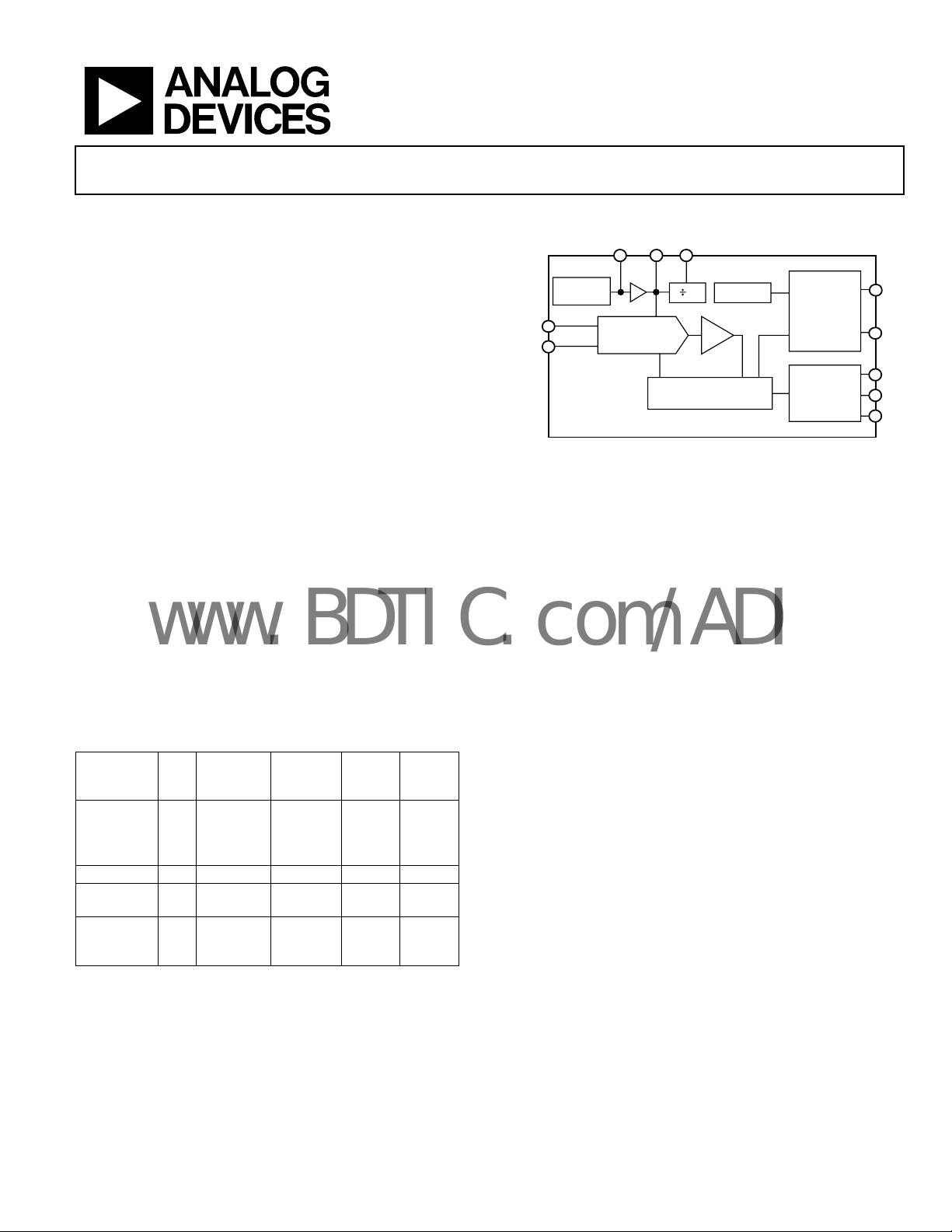
FUNCTIONAL BLOCK DIAGRAM
REFIN REF
1.2V
BANDGAP
IN+
IN-
CAP DAC
AD7626
GENERAL DESCRIPTION
The AD7626 is a 16-bit, 10MSPS, charge redistribution
successive approximation register (SAR) architecture, analogto-digital converter (ADC). SAR architecture allows unmatched
performance both in noise – 92dB SNR - and in linearity –
1LSB. The AD7626 contains a high speed 16-bit sampling ADC,
an internal conversion clock, and an internal buffered reference.
On the CNV edge, it samples the voltage difference between
IN+ and IN− pins. The voltages on these pins swing in opposite
phase between 0 V and REF. The 4.096V reference voltage, REF,
can be generated internally or applied externally.
All converted results are available on a single LVDS self-clocked
or echoed-clock serial interface reducing external hardware
connections.
The AD7626 is housed in a 32-lead LFCSP (5mm by 5mm) with
operation specified from −40°C to +85°C.
CM
2
SAR
Figure 1.
CLOCK
LOGIC
SERIAL
LVDS
VIO
CNV
D
DCO
CLK
Rev. PrC
Information furnished by Analog Devices is believed to be accurate and reliable. However, no
responsibility is assumed by Anal og Devices for its use, nor for any infringements of patents or ot her
rights of third parties that may result from its use. Specifications subject to change without notice. No
license is granted by implication or otherwise under any patent or patent rights of Analog Devices.
Trademarks and registered trademarks are the property of their respective owners.
One Technology Way, P.O. Box 9106, Norwood, MA 02062-9106, U.S.A.
Tel: 781.329.4700 www.analog.com
Fax: 781.461.3113 ©2008 Analog Devices, Inc. All rights reserved.
Page 2

AD7626 Preliminary Technical Data
www.BDTIC.com/ADI
TABLE OF CONTENTS
Features.............................................................................................. 1
Applications....................................................................................... 1
Functional Block Diagram .............................................................. 1
General Description ......................................................................... 1
Specifications..................................................................................... 3
Timing Specifications .................................................................. 4
Absolute Maximum Ratings............................................................ 5
Thermal Resistance.......................................................................5
ESD Caution...................................................................................5
Pin Configuration and Function Descriptions..............................6
Terminology.......................................................................................8
Theory of Operation .........................................................................9
Outline Dimensions....................................................................... 11
Rev. PrC | Page 2 of 11
Page 3
Preliminary Technical Data AD7626
www.BDTIC.com/ADI
SPECIFICATIONS
VDD1 = 5 V; VDD2 = 2.5 V; VIO = 2.5 V; V
Table 2.
Parameter Conditions Min Typ Max Unit
RESOLUTION 16 Bits
ANALOG INPUT
Voltage Range V
Operating Input Voltage V
Common Mode Input Range V
Analog Input CMRR fIN = 1 MHz 60 dB
Input Current 10 MSPS throughput 550 μA
THROUGHPUT SPEED
Complete Cycle 100 ns
Throughput Rate 0.001 10 MSPS
DC ACCURACY
Integral Linearity Error -2 ±1 +2 LSB
No Missing Codes 16 Bits
Differential Linearity Error -1 ±0.3 +1 LSB
Transition Noise 0.6 LSB
Zero Error, T
MIN
to T
±100 μV
MAX
Zero Error Drift 1 ppm/°C
Gain Error, T
MIN
to T
50 ppm of FS
MAX
Gain Error Drift 1 ppm/°C
Power Supply Sensitivity VDD1 = 5 V ± 5% TBD LSB
VDD2 = 2.5 V ± 5% TBD LSB
AC ACCURACY
Dynamic Range 90 92 dB
Signal-to-Noise fIN = 1 MHz 90 92 dB
Spurious-Free Dynamic Range fIN = 1 MHz 110 dB
f
Total Harmonic Distortion fIN = 1 MHz -110 dB
f
Signal-to-(Noise + Distortion) fIN = 1 MHz 92 dB
−3 dB Input Bandwidth 100 MHz
Aperture Delay ns
Aperture jitter 5 ps rms
Transient Response Full-Scale Step 50 ns
INTERNAL REFERENCE
Output Voltage REFIN @ 25°C 1.2 V
Temperature Drift −40°C to +85°C ±7 ppm/°C
REFERENCE BUFFER
REFIN Input Voltage Range 1.2 V
REF Output Voltage range 4.096 V
EXTERNAL REFERENCE
Voltage Range REF 4.096 V
VCM @ 25°C
Output Voltage V
Output Impedance 4 5 6 kΩ
= 4.096 V; all specifications T
REF
− V
IN+
IN+
IN
IN
−V
IN−
, V
to AGND −0.1 +V
IN−
= TBD 90 dB
= TBD -90 dB
MIN
to T
, unless otherwise noted.
MAX
+V
REF
/2 – 0.1 V
REF
REF
REF
V
REF
+ 0.1 V
REF
/2 V
/2 + 0.1 V
REF
/2 V
REF
/2
Rev. PrC | Page 3 of 11
Page 4
AD7626 Preliminary Technical Data
www.BDTIC.com/ADI
Parameter Conditions Min Typ Max Unit
LVDS I/O, (ANSI-644)
Data Format Serial LVDS Two’s complement
VOD Differential Output Voltage,
=100 Ω
R
L
V
OCM
Common mode Output Voltage,
=100Ω
R
L
247 350 454 mV
1125 1250 1375 mV
VID Differential Input Voltage 100 650 mV
V
Common mode Input Voltage 800 1575 mV
ICM
POWER SUPPLIES
Specified Performance
VDD1 4.75V 5 5.25V V
VDD2 2.37 2.5 2.63 V
VIO 2.3 2.5 2.7 V
Operating Currents
VDD1 10 mA
VDD2 25 mA
VIO Self-clocked mode 14 mA
VIO Echoed-clock mode 18 mA
Power Dissipation1
With Internal Reference 10 MSPS throughput 140 mW
Without Internal Reference 10 MSPS throughput 120 mW
Energy per conversion 10 MSPS throughput 10 nJ/sample
TEMPERATURE RANGE
Specified Performance T
1
Power dissipation is for the AD7626 only. In self-clocked interface, 9mW is dissipated in the 100 ohm terminator. In echoed-clock interface, 18mW is dissipated in (2)
100 ohm terminators.
MIN
to T
−40 +85 °C
MAX
TIMING SPECIFICATIONS
VDD1 = 5 V; VDD2 = 2.5 V; VIO = 2.3V to 2.7 V; V
Table 3.
Parameter Symbol Min Typ Max Unit
Time between conversion t
Acquisition time t
CNV high time t
CNV to D (MSB) delay t
CNV to last CLK (LSB) delay t
CLK period t
CLK frequency f
CLK to DCO delay (echoed-clock mode) t
DCO to D delay (echo-clock mode) tD -1 0 1 ns
CLK to D delay t
= 4.096 V; all specifications T
REF
100 ns
CYC
40 10000 ns
ACQ
10 40 ns
CNVH
100 ns
MSB
64 ns
CLKL
TBD 4 ns
CLK
250 400 MHz
CLK
0 4 7 ns
DCO
0 4 7 ns
CLKD
MIN
to T
, unless otherwise noted.
MAX
Rev. PrC | Page 4 of 11
Page 5

Preliminary Technical Data AD7626
www.BDTIC.com/ADI
ABSOLUTE MAXIMUM RATINGS
Table 4.
Parameter With
Respect to
Analog Inputs/Outputs
CAP1, REFIN GND -0.3V to 2.7V
IN+, IN-, REF, REF/2,
CAP2
Digital Inputs/Outputs GND -0.3V to 2.7V
Supply Voltage
VDD1 GND -0.3V to 6V
VDD2, VIO GND -0.3V to 2.7V
Stresses above those listed under Absolute Maximum Ratings
may cause permanent damage to the device. This is a stress
rating only; functional operation of the device at these or any
other conditions above those indicated in the operational
section of this specification is not implied. Exposure to absolute
GND -0.3V to 6V
Rating
maximum rating conditions for extended periods may affect
device reliability.
THERMAL RESISTANCE
θJA is specified for the worst-case conditions, that is, a device
soldered in a circuit board for surface-mount packages.
Table 5. Thermal Resistance
Package Type θJA θ
Unit
JC
ESD CAUTION
Rev. PrC | Page 5 of 11
Page 6

AD7626 Preliminary Technical Data
www.BDTIC.com/ADI
PIN CONFIGURATION AND FUNCTION DESCRIPTIONS
2
ND
G
CAP2
CAP
REF
REF
REF
GND
29
30
31
32
CAP2
6
27
2
28
25
1VDD1
2VDD2
3CAP1
4REFIN
5EN0
6EN1
7VDD2
8CNV-
PIN 1
INDICATOR
TOP VIEW
9
10
D-
CNV+
11
12
IO
D+
V
Figure 2.
4
13
1
GND
DCO-
15
DCO+
24 GND
23 IN+
22 IN21 REF/2
20 VDD1
19 VDD1
18 VDD2
17 CLK+
16
CLK-
Table 6. Pin Function Descriptions
Pin No. Mnemonic Type1 Description
1 VDD1 P Analog 5V Supply.
Decouple with 10uF and 100nF capacitors.
2 VDD2 P Analog 2.5V Supply.
The system 2.5V supply should supply this pin first, decoupled with 10uF and 100nF capacitors, then
starred off to other VDD2 pins.
3 CAP1 AO Connect to a 10nF capacitor.
4 REFIN AI/O Pre-Buffer Reference Voltage.
When using the internal reference, this pin outputs the band-gap voltage and is nominally at 1.2V. It can
be overdriven with an external reference voltage like the ADR280.
In either mode, a 10uF capacitor is required. If using an external 4.096V reference (connected to REF), this
pin is a no connect and does not require any capacitor.
5, 6 EN0, EN1
DI Enable Pins.
EN1 EN0 Operation
0 0 Power down all; ADC, internal reference and reference buffer.
0 1
Enable internal buffer, disable internal reference. An external 1.2V reference
connected to REFIN pin is required.
1 0
Disable internal reference and buffer. An external reference connected to the REF
pin is required.
1 1 Enable all; ADC, internal reference and reference buffer.
7 VDD2 P Digital 2.5V supply.
8, 9 CNV-, CNV+ DI Convert Input.
This input has multiple functions. On its rising edge, it samples the analog inputs and initiates a
conversion cycle. CNV+ works as a CMOS input when CNV- is grounded otherwise CNV+, CNV- are LVDS
inputs.
10, 11 D-, D+ D0 LVDS Data Outputs.
The conversion data is output serially on these pins.
12 VIO P Input/Output Interface Supply. Nominally 2.5V.
13 GND P Ground.
14, 15 DCO-, DCO+ DI/O LVDS Buffered Clock Outputs.
When DCO+ is grounded, the self-clock interface mode is selected. In this mode, the 16 bit results on D
is preceded by a three bit header (010) to allow synchronization of the data by the digital host with
simple logic.
When DCO+ is not grounded, the echoed clock interface mode is selected. In this mode, DCO± is a copy
of CLK±. The data bits are output on the falling edge of DCO+ and can be latched in the digital host on
the next rising edge of DCO+.
16, 17 CLK-, CLK+ DI LVDS Clock Inputs.
This clock shifts out the conversion results on the negative edge of CLK+.
00000-000
Rev. PrC | Page 6 of 11
Page 7

Preliminary Technical Data AD7626
www.BDTIC.com/ADI
Pin No. Mnemonic Type1 Description
18 VDD2 P Analog 2.5V Supply.
19, 20 VDD1 P Analog 5V supply. Isolate from Pin 1 with a ferrite bead.
21 VCM AO Common Mode Output.
When using any reference scheme, this pin produces ½ of the voltage present on the REF pin which can
be useful for driving the common mode of the input amplifiers.
22 IN- AI Differential Negative Analog Input.
Referenced to and must be driven 180° out of phase with IN+.
23 IN+ AI Differential Positive Analog Input.
Referenced to and must be driven 180° out of phase with IN-.
24 GND P Ground.
25, 26,
28
27 GND P Ground.
29, 30,
32
31 GND P Ground.
1
AI = analog input; AI/O = bidirectional analog; AO = analog output; DI = digital input; DI/O = bidirectional digital; DO = digital output; P = power.
CAP2 AO
REF AI/O Buffered Reference Voltage.
Connect all three pins to a single 10uF X5R capacitor with the shortest distance. The other side of the
capacitor must be placed close to pin 27 (GND).
Return path for 10uF capacitor connected to pins 25, 26, and 28.
When using the internal reference or 1.2V external reference (REFIN input), the 4.096V system reference
is produced at this pin.
When using an external reference, like the ADR434 or ADR444, the internal reference buffer must be
disabled.
In either case, connect all three pins to a single 10uF X5R capacitor with the shortest distance. The other
side of the capacitor must be placed close to pin 31 (GND)
Return path for 10uF capacitor connected to pins 29, 30, and 32.
Rev. PrC | Page 7 of 11
Page 8

AD7626 Preliminary Technical Data
V
www.BDTIC.com/ADI
TERMINOLOGY
Least Significant Bit (LSB)
The least significant bit, or LSB, is the smallest increment that
can be represented by a converter. For a fully differential input
ADC with N bits of resolution, the LSB expressed in volts is
INp-p
VLSB2)( =
N
Integral Nonlinearity Error (INL)
Linearity error refers to the deviation of each individual code
from a line drawn from negative full scale through positive fullscale. The point used as negative full scale occurs a ½ LSB before
the first code transition. Positive full scale is defined as a level
1½ LSBs beyond the last code transition. The deviation is measured from the middle of each code to the true straight line.
Differential Nonlinearity Error (DNL)
In an ideal ADC, code transitions are 1 LSB apart. Differential
nonlinearity is the maximum deviation from this ideal value. It
is often specified in terms of resolution for which no missing
codes are guaranteed.
Zero Error
The difference between the ideal midscale input voltage (0 V)
and the actual voltage producing the midscale output code.
Gain Error
The first transition (from 100 ... 00 to 100 ... 01) should occur at
a level ½ LSB above nominal negative full scale (−4.095938 V
for the ±4.096V V range). The last transition (from 011 … 10 to
011 … 11) should occur for an analog voltage 1½ LSB below the
nominal full scale (+4.095813 V for the ±4.096V range). The
gain error is the deviation of the difference between the actual
level of the last transition and the actual level of the first
transition from the difference between the ideal levels.
Dynamic Range
Dynamic range is the ratio of the rms value of the full scale to
the rms noise measured for an input typically at −60 dB. The
value for dynamic range is expressed in decibels.
Signal-to-Noise Ratio (SNR)
SNR is the ratio of the rms value of the actual input signal to
the rms sum of all other spectral components below the Nyquist
frequency, excluding harmonics and dc. The value for SNR is
expressed in decibels.
Total Harmonic Distortion (THD)
THD is the ratio of the rms sum of the first five harmonic
components to the rms value of a full-scale input signal and
is expressed in decibels.
Signal-to-(Noise + Distortion) Ratio (SINAD)
SINAD is the ratio of the rms value of the actual input signal to
the rms sum of all other spectral components below the Nyquist
frequency, including harmonics but excluding dc. The value for
SINAD is expressed in decibels.
Spurious-Free Dynamic Range (SFDR)
The difference, in decibels (dB), between the rms amplitude of
the input signal and the peak spurious signal.
Effective Number of Bits (ENOB)
ENOB is a measurement of the resolution with a sine wave
input. It is related to SINAD and is expressed in bits by
ENOB = [(SINAD
− 1.76)/6.02]
dB
Aperture Delay
Aperture delay is a measure of the acquisition performance
measured from the falling edge of the
CNVST
input to when
the input signal is held for a conversion.
Transient Response
The time required for the AD7634 to achieve its rated accuracy
after a full-scale step function is applied to its input.
Reference Voltage Temperature Coefficient
Reference voltage temperature coefficient is derived from the
typical shift of output voltage at 25°C on a sample of parts at
the maximum and minimum reference output voltage (V
measured at T
MIN
REF
, T(25°C), and T
Cppm/ ×
=°
)(TCV
REF
. It is expressed in ppm/°C as
MAX
((
REFREF
C25
×°
MAX
MIN
)MinV–)MaxV
)T–T()(V
where:
V
(Max) = maximum V
REF
(Min) = minimum V
V
REF
V
(25°C) = V
REF
= +85°C.
T
MAX
T
= –40°C.
MIN
at 25°C.
REF
REF
REF
at T
at T
MIN
, T(25°C), or T
MIN
, T(25°C), or T
MAX
MAX
)
REF
6
10
.
.
Rev. PrC | Page 8 of 11
Page 9

Preliminary Technical Data AD7626
www.BDTIC.com/ADI
THEORY OF OPERATION
Echoed-Clock Interface Mode
The AD7626 digital operation in “echoed-clock interface mode”
is shown in Figure 3. This interface mode, requiring just a shift
register on the digital host, can be used with many digital hosts
(FPGA, shift register, microprocessor, etc.). It requires 3 LVDS
pairs (D±, CLK±, and DCO±) between each AD7626 and the
digital host.
The clock DCO is a buffered copy of CLK and synchronous to
the data, D, which is updated on DCO+ falling edge (t
). By
D
keeping good propagation delay matching between D and DCO
through the board and the digital host, DCO can be can be used
to latch D with good timing margin for the shift register.
CNV-
SAMPLE N
T
CNVH
T
CYC
Conversions are initiated by a CNV pulse. The CNV must be
returned low ≤ t
(max) for valid operation. Once a
CNVH
conversion has begun, it continues until completion. Additional
CNV pulses are ignored during the conversion phase. After the
time t
that t
elapses, the host should begin to burst the CLK. Note
MSB
is the maximum time for the MSB of the new
MSB
conversion result and should be used as the gating device for
CLK. The echoed clock, DCO, and data, D, will be driven in
phase with D being updated on the DCO+ falling edge and the
host should use the DCO+ rising edge to capture D. The only
requirement is that the 16 CLK pulses finish before the time
t
elapses of the next conversion phase or the data will be lost.
CLKL
From the time t
SAMPLE N+1
CLKL
to t
, D and DCO will be driven to 0’s.
MSB
CNV+
CLK-
CLK+
DCO-
DCO+
D+
D-
ACQUISITION
T
CLK
T
DCO
T
CLKD
D1
N-1
T
ACQ
ACQUISITION ACQUISITION
1615
1615 116152
T
MSB
D0
N-1
0
Figure 3. Echoed-Clock Interface Mode Timing Diagram
116152
T
D15
N
D
D14
N
T
CLKL
D1
1
23
1
23
D0
N
N
0
D15
N+1
D14
N+1
D13
N+1
Rev. PrC | Page 9 of 11
Page 10

AD7626 Preliminary Technical Data
www.BDTIC.com/ADI
Self Clocked Mode
The AD7626 digital operation in “self-clocked interface mode”
is shown in Figure 4. This interface mode reduces the number
of wires between ADCs and the digital host to 2 LVDS pairs per
AD7626, CLK± and D± or a single pair if sharing a common
CLK using multiple AD7626’s. This considerably eases the
design of a system using multiple AD7626’s since the interface
can tolerate several CLK cycles of propagation delay mismatch
between the different AD7626 devices and the digital host.
The “self-clocked interface mode” consists of preceding each
ADC word results by a header of 2 bits on the data, D This
header is used to synchronize D of each conversion in the
digital host. Synchronization is accomplished by one simple
state machine per AD7626 device. The state machine is running,
for instance, at the same speed as CLK with 3 phases. The state
machine measures when the first “one” of the header occurs.
This provides the value of the actual propagation delay delta
SAMPLE N
T
CNVH
T
CYC
between the state machine clock and D including any board
propagation time allowing to use the best clock signal to latch
the following bits of the conversion result.
Conversions are initiated by a CNV pulse. The CNV must be
returned low ≤ t
(max) for valid operation. Once a
CNVH
conversion has begun, it continues until completion. Additional
CNV pulses are ignored during the conversion phase. After the
time t
that t
elapses, the host should begin to burst the CLK. Note
MSB
is the maximum time for the first bit of the header and
MSB
should be used as the gating device for CLK. CLK is also used
internally on the host to begin the internal synchronization
state machine. The next header bit and conversion results are
output on subsequent falling edges of CLK. The only
requirement is that the 18 CLK pulses finish before the time
t
elapses of the next conversion phase or the data will be
CLKL
lost.
SAMPLE N+1
CNV-
CNV+
T
ACQ
ACQUISITION
T
CLK
CLK-
CLK+
T
CLKD
D+
D-
1
This timing is for silicon rev 1 or above. For silicon rev 0, there is an extra bit (a zero) in front on the bit with value 1. Therefore, silicon rev 0 needs 19 clock pulses.
1817 142
T
MSB
D1
N-1
D0
N-1
Figure 4. Self-Clocked Interface Mode Timing Diagram1
ACQUISITION
*1
00
1
D15ND14
N
T
CLKL
D1
18173
D0
N
N
ACQUISITION
1
0
1
23
0
D15
N+1
Rev. PrC | Page 10 of 11
Page 11

Preliminary Technical Data AD7626
www.BDTIC.com/ADI
OUTLINE DIMENSIONS
0.60 MAX
25
24
EXPOSED
PAD
(BOTTOM VIEW)
17
16
32
1
8
9
3.50 REF
PIN 1
INDICATOR
3.45
3.30 SQ
3.15
0.25 MIN
PIN 1
INDICATOR
1.00
0.85
0.80
12° MAX
SEATING
PLANE
5.00
BSC SQ
TOP
VIEW
0.80 MAX
0.65 TYP
0.30
0.23
0.18
COMPLIANT TO JEDEC STANDARDS MO-220-VHHD-2
4.75
BSC SQ
0.20 REF
0.05 MAX
0.02 NOM
0.60 MAX
0.50
BSC
0.50
0.40
0.30
COPLANARITY
0.08
Figure 5.32-Lead Lead Frame Chip Scale package [LFCSP_VQ]
5 mm × 5 mm Body, Very Thin Quad
(CP-32-3)
©2008 Analog Devices, Inc. All rights reserved. Trademarks and
registered trademarks are the property of their respective owners.
PR07648-0-6/08(PrC)
 Loading...