

Page 1
LC2MOS
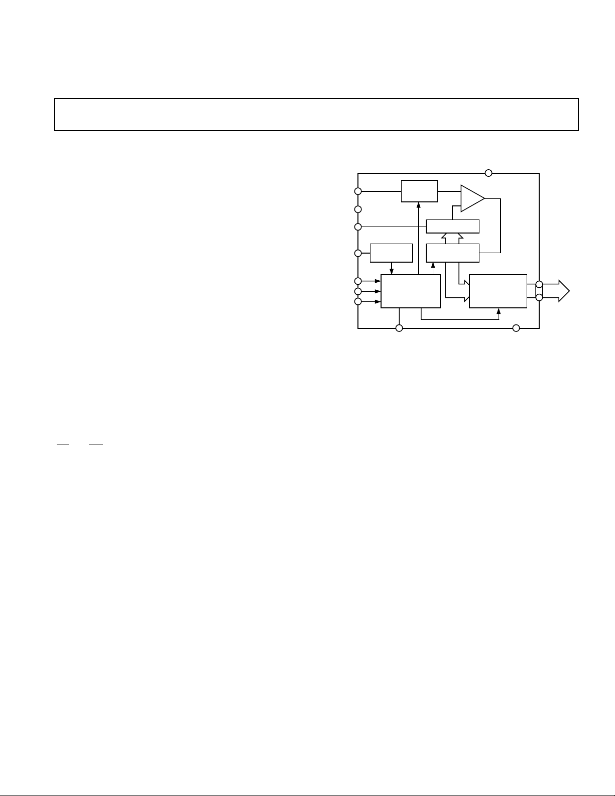
TRACK
AND
HOLD
CLOCK
OSCILLATOR
DAC
SAR
COMP
CONTROL
LOGIC
LATCH AND
THREE STATE
OUTPUT DRIVERS
AD7575
V
DD
AIN
AGND
V
REF
CLK
CS
RD
TP
BUSY
DGND
DB7
DB0
a
FEATURES
Fast Conversion Time: 5 s
On-Chip Track/Hold
Low Total Unadjusted Error: 1 LSB
Full Power Signal Bandwidth: 50 kHz
Single +5 V Supply
100 ns Data Access Time
Low Power (15 mW typ)
Low Cost
Standard 18-Lead DlPs or 20-Terminal
Surface Mount Packages
GENERAL DESCRIPTION
The AD7575 is a high speed 8-bit ADC with a built-in track/
hold function. The successive approximation conversion tech-
nique is used to achieve a fast conversion time of 5 µs, while the
built-in track/hold allows full-scale signals up to 50 kHz (386 mV/µs
slew rate) to be digitized. The AD7575 requires only a single +5 V
supply and a low cost, 1.23 V bandgap reference in order to convert
an input signal range of 0 to 2 V
The AD7575 is designed for easy interfacing to all popular 8-bit
microprocessors using standard microprocessor control signals
(
CS and RD) to control starting of the conversion and reading of
the data. The interface logic allows the AD7575 to be easily
configured as a memory mapped device, and the part can be
interfaced as SLOW-MEMORY or ROM. All data outputs of
the AD7575 are latched and three-state buffered to allow direct
connection to a microprocessor data bus or I/O port.
The AD7575 is fabricated in an advanced, all ion-implanted high
speed Linear Compatible CMOS (LC
available in a small, 0.3" wide, 18-lead DIP, 18-lead SOIC or in
other 20-terminal surface mount packages.
REF
.
2
MOS) process and is
5 s 8-Bit ADC with Track/Hold
AD7575
FUNCTIONAL BLOCK DIAGRAM
PRODUCT HIGHLIGHTS
1. Fast Conversion Time/Low Power
The fast, 5 µs, conversion time of the AD7575 makes it
suitable for digitizing wideband signals at audio and ultrasonic frequencies while retaining the advantage of low
CMOS power consumption.
2. On-Chip Track/Hold
The on-chip track/hold function is completely self-contained
and requires no external hold capacitor. Signals with slew
rates up to 386 mV/µs (e.g., 2.46 V peak-to-peak 50 kHz sine
waves) can be digitized with full accuracy.
3. Low Total Unadjusted Error
The zero, full-scale and linearity errors of the AD7575 are so
low that the total unadjusted error at any point on the transfer function is less than 1 LSB, and offset and gain adjustments are not required.
4. Single Supply Operation
Operation from a single +5 V supply with a low cost +1.23 V
bandgap reference allows the AD7575 to be used in 5 V
microprocessor systems without any additional power
supplies.
5. Fast Digital Interface
Fast interface timing allows the AD7575 to interface easily to
the fast versions of most popular microprocessors such as the
Z80H, 8085A-2, 6502B, 68B09 and the DSP processor, the
TMS32010.
REV. B
Information furnished by Analog Devices is believed to be accurate and
reliable. However, no responsibility is assumed by Analog Devices for its
use, nor for any infringements of patents or other rights of third parties
which may result from its use. No license is granted by implication or
otherwise under any patent or patent rights of Analog Devices.
One Technology Way, P.O. Box 9106, Norwood, MA 02062-9106, U.S.A.
Tel: 781/329-4700 World Wide Web Site: http://www.analog.com
Fax: 781/326-8703 © Analog Devices, Inc., 1998
Page 2

AD7575–SPECIFICATIONS
(VDD = +5 V, V
all specifications T
= +1.23 V, AGND = DGND = 0 V; f
REF
to T
MIN
unless otherwise noted)
MAX
= 4 MHz external;
CLK
Parameter J, A Versions1K, B Versions S Version T Version Units Conditions/Comments
ACCURACY
Resolution 8 8 8 8 Bits
Total Unadjusted Error ±2 ±1 ±2 ±1 LSB max
Relative Accuracy ±1 ±1/2 ±1 ±1/2 LSB max
Minimum Resolution for Which
No Missing Codes Is Guaranteed 8 8 8 8 Bits max
Full-Scale Error
+25°C ±1 ±1 ±1 ±1 LSB max Full-Scale TC Is Typically 5 ppm/°C
T
to T
MIN
Offset Error
MAX
2
±1 ±1 ±1 ±1 LSB max
+25°C ±1/2 ±1/2 ±1/2 ±1/2 LSB max Offset TC Is Typically 5 ppm/°C
T
MIN
to T
MAX
±1/2 ±1/2 ±1/2 ±1/2 LSB max
ANALOG INPUT
Voltage Range 0 to 2 V
REF
0 to 2 V
REF
0 to 2 V
REF
0 to 2 V
Volts 1 LSB = 2 V
REF
/256; See Figure 16
REF
DC Input Impedance 10 10 10 10 MΩ min
Slew Rate, Tracking 0.386 0.386 0.386 0.386 V/µs max
3
SNR
45 45 45 45 dB min VIN = 2.46 V p-p @ 10 kHz; See Figure 11
REFERENCE INPUT
V
(For Specified Performance) 1.23 1.23 1.23 1.23 Volts ±5%
REF
I
REF
500 500 500 500 µA max
LOGIC INPUTS
CS, RD
V
, Input Low Voltage 0.8 0.8 0.8 0.8 V max
INL
V
, Input High Voltage 2.4 2.4 2.4 2.4 V min
INH
IIN, Input Current
+25°C ±1 ±1 ±1 ±1 µA max V
T
to T
MIN
MAX
CIN, Input Capacitance
3
±10 ±10 ±10 ±10 µA max V
10 10 10 10 pF max
= 0 or V
IN
= 0 or V
IN
DD
DD
CLK
V
, Input Low Voltage 0.8 0.8 0.8 0.8 V max
lNL
V
, Input High Voltage 2.4 2.4 2.4 2.4 V min
INH
I
, Input Low Current 700 700 800 800 µA max V
INL
I
, Input High Current 700 700 800 800 µA max V
INH
INL
INH
= 0 V
= V
DD
LOGIC OUTPUTS
BUSY, DB0 to DB7
VOL, Output Low Voltage 0.4 0.4 0.4 0.4 V max I
VOH, Output High Voltage 4.0 4.0 4.0 4.0 V min I
= 1.6 mA
SINK
SOURCE
= 40 µA
DB0 to DB7
Floating State Leakage Current ±1 ±1 ±10 ±10 µA max V
OUT
= 0 to V
DD
Floating State Output Capacitance310 10 10 10 pF max
CONVERSION TIME
With External Clock 5 5 5 5 µsf
With Internal Clock, T
4
= 4 MHz
= +25°C5 5 5 5 µs min Using Recommended Clock
A
CLK
15 15 15 15 µs max Components Shown in Figure 15
POWER REQUIREMENTS
V
DD
I
DD
5
+5 +5 +5 +5 Volts ±5% for Specified Performance
6 6 7 7 mA max Typically 3 mA with VDD = +5 V
Power Dissipation 15 15 15 15 mW typ
Power Supply Rejection ±1/4 ±1/4 ±1/4 ±1/4 LSB max 4.75 V ≤ VDD ≤ 5.25 V
NOTES
1
Temperature ranges are as follows:
J, K Versions; 0°C to +70°C
A, B Versions; –25°C to +85°C
S, T Versions; –55°C to +125°C
2
Offset error is measured with respect to an ideal first code transition that occurs at 1/2 LSB.
3
Sample tested at +25°C to ensure compliance.
4
Accuracy may degrade at conversion times other than those specified.
5
Power supply current is measured when AD7575 is inactive i.e., when CS = RD = BUSY = logic HIGH.
Specifications subject to change without notice.
–2–
REV. B
Page 3
AD7575
WARNING!
ESD SENSITIVE DEVICE
DGND
3kV 10pF
DBN
TIMING SPECIFICATIONS
Limit at +25ⴗC Limit at T
1
(VDD = +5 V, V
MIN
= +1.23 V, AGND = DGND = 0 V)
REF
, T
MAX
Limit at T
MIN
, T
MAX
Parameter (All Versions) (J, K, A, B Versions) (S, T Versions) Units Conditions/Comments
t
1
t
2
2
t
3
t
4
t
5
2
t
6
3
t
7
0 0 0 ns min CS to RD Setup Time
100 100 120 ns max RD to BUSY Propagation Delay
100 100 120 ns max Data Access Time after RD
100 100 120 ns min RD Pulse Width
0 0 0 ns min CS to RD Hold Time
80 80 100 ns max Data Access Time after BUSY
10 10 10 ns min Data Hold Time
80 80 100 ns max
t
8
NOTES
1
Timing specifications are sample tested at +25°C to ensure compliance. All input control signals are specified with tr = tf = 20 ns (10% to 90% of +5 V)
and timed from a voltage level of 1.6 V.
2
t3 and t6 are measured with the load circuits of Figure 1 and defined as the time required for an output to cross 0.8 V or 2.4 V.
3
t7 is defined as the time required for the data lines to change 0.5 V when loaded with the circuits of Figure 2.
Specifications subject to change without notice.
0 0 0 ns min BUSY to CS Delay
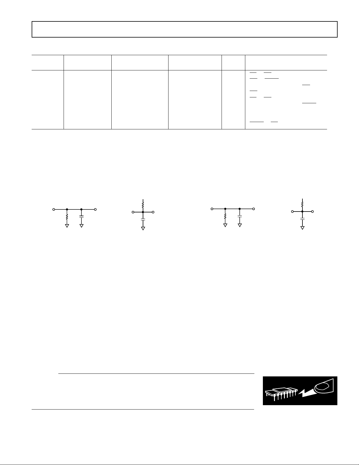
Test Circuits
+5V
3kV
DBN
10pF
DGND
DBN
3kV 100pF
DGND
+5V
3kV
DBN
100pF
DGND
a. High-Z to V
OH
b High-Z to V
OL
a. VOH to High-Z b. VOL to High-Z
Figure 1. Load Circuits for Data Access Time Test Figure 2. Load Circuits for Data Hold Time Test
ABSOLUTE MAXIMUM RATINGS*
VDD to AGND . . . . . . . . . . . . . . . . . . . . . . . . . . . –0.3 V, +7 V
V
to DGND . . . . . . . . . . . . . . . . . . . . . . . . . . . –0.3 V, +7 V
DD
AGND to DGND . . . . . . . . . . . . . . . . . . . . . . . . –0.3 V, V
DD
Digital Input Voltage to DGND . . . . . . . –0.3 V, VDD + 0.3 V
Digital Output Voltage to DGND . . . . . . –0.3 V, V
CLK Input Voltage to DGND . . . . . . . . . –0.3 V, V
to AGND . . . . . . . . . . . . . . . . . . . . . . . . . . –0.3 V, V
V
REF
AIN to AGND . . . . . . . . . . . . . . . . . . . . . . . . . . . –0.3 V, V
+ 0.3 V
DD
+ 0.3 V
DD
DD
DD
Operating Temperature Range
Storage Temperature Range . . . . . . . . . . . . –65°C to +150°C
Lead Temperature (Soldering, 10 sec) . . . . . . . . . . . . +300°C
Power Dissipation (Any Package) to +75°C . . . . . . . 450 mW
Derates above +75°C by . . . . . . . . . . . . . . . . . . . . . 6 mW/°C
*Stresses above those listed under Absolute Maximum Ratings may cause perma-
nent damage to the device. This is a stress rating only; functional operation of the
device at these or any other conditions above those indicated in the operational
sections of this specification is not implied. Exposure to absolute maximum rating
conditions for extended periods may affect device reliability.
Commercial (J, K Versions) . . . . . . . . . . . . . . 0°C to +70°C
Industrial (A, B Versions) . . . . . . . . . . . . . –25°C to +85°C
Extended (S, T Versions) . . . . . . . . . . . . . –55°C to +125°C
CAUTION
ESD (electrostatic discharge) sensitive device. Electrostatic charges as high as 4000 V readily
accumulate on the human body and test equipment and can discharge without detection.
Although the AD7575 features proprietary ESD protection circuitry, permanent damage may
occur on devices subjected to high energy electrostatic discharges. Therefore, proper ESD
precautions are recommended to avoid performance degradation or loss of functionality.
REV. B
–3–
Page 4
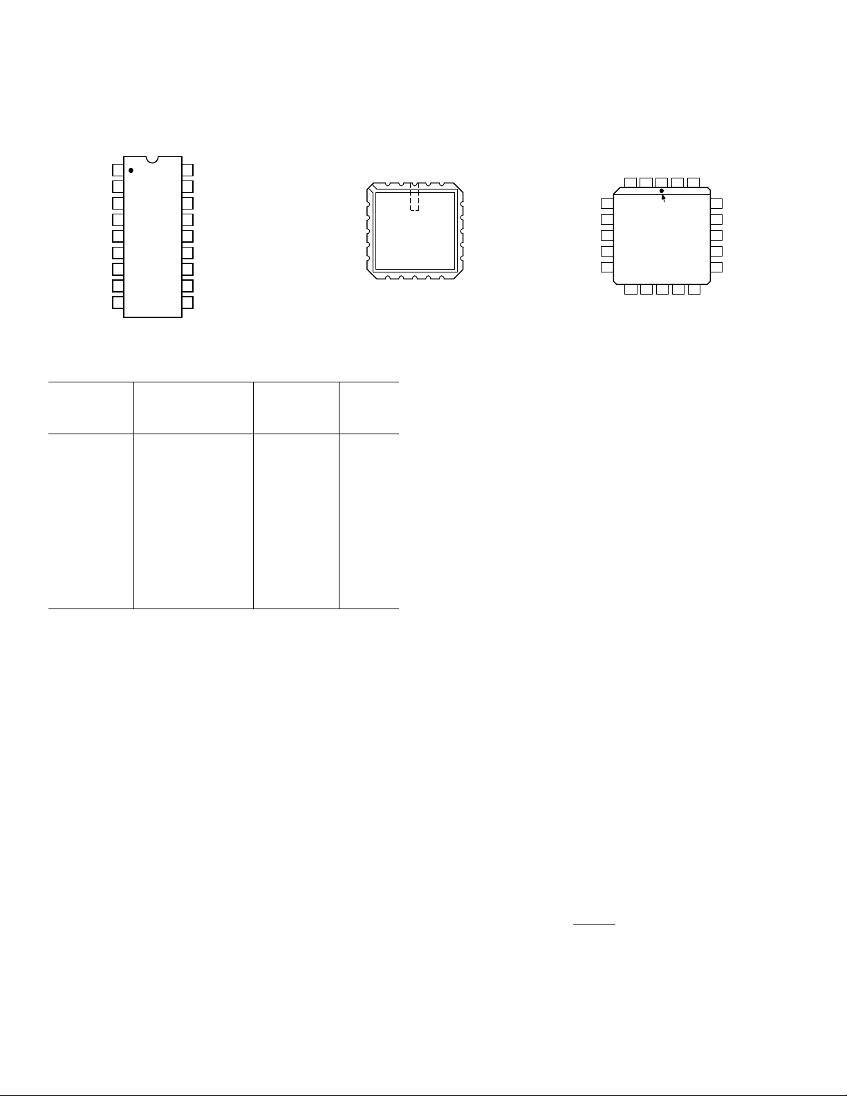
AD7575
PIN CONFIGURATIONS
LCCC
CS
RD
BUSY
CLK
DB7 (MSB)
DB6
DB5
DGND
TP
1
2
3
4
AD7575
5
TOP VIEW
(Not to Scale)
6
7
8
9
18
V
17
V
16
AIN
15
AGND
14
DB0 (LSB)
13
DB1
12
DB2
11
DB3
10
DB4
DD
REF
BUSY
CLK
DB7 (MSB)
DB6
DB5
NC = NO CONNECT
3
4
5
6
(Not to Scale)
7
8
9 10111213
TPRDCS
2
AD7575
TOP VIEW
DGND
ORDERING GUIDE
Relative
Temperature Accuracy Package
Range (LSB) Options
2
Model
1
AD7575JR 0°C to +70°C ±1 max R-18
AD7575JN 0°C to +70°C ±1 max N-18
AD7575KN 0°C to +70°C ±1/2 max N-18
AD7575JP 0°C to +70°C ±1 max P-20A
AD7575KP 0°C to +70°C ±1/2 max P-20A
AD7575AQ –25°C to +85°C ±1 max Q-18
AD7575BQ –25°C to +85°C ±1/2 max Q-18
AD7575SQ –55°C to +125°C ±1 max Q-18
AD7575TQ –55°C to +125°C ±1/2 max Q-18
AD7575SE –55°C to +125°C ±1 max E-20A
AD7575TE –55°C to +125°C ±1/2 max E-20A
NOTES
1
To order MIL-STD-883, Class B process parts, add /883B to part number.
Contact local sales office for military data sheet. For U.S. Standard Military
Drawing (SMD), see DESC drawing #5962-87762.
2
E = Leadless Ceramic Chip Carrier; N = Plastic DIP; P = Plastic Leaded Chip
Carrier; Q = Cerdip, R = SOIC.
PLCCDIP/SOIC
NC
NC
20 191
VDDV
DB4
REF
DB3
18
AIN
AGND
17
16
DB0 (LSB)
15
DB1
14
DB2
4
TP
5
BUSY
6
CLK
DB6
7
8
DB7 (MSB)
NC = NO CONNECT
RDCSNC
3 2 1 20 19
AD7575
TOP VIEW
(Not to Scale)
9 10 11 12 13
DB5
DGND
VDDV
PIN 1
IDENTIFIER
NC
DB4
REF
DB3
18
AIN
17
AGND
16
DB0 (LSB)
15
DB1
14
DB2
TERMINOLOGY
LEAST SIGNIFICANT BIT (LSB)
An ADC with 8-bits resolution can resolve 1 part in 28 (i.e.,
256) of full scale. For the AD7575 with +2.46 V full-scale one
LSB is 9.61 mV.
TOTAL UNADJUSTED ERROR
This is a comprehensive specification that includes full-scale
error, relative accuracy and offset error.
RELATIVE ACCURACY
Relative Accuracy is the deviation of the ADC’s actual code
transition points from a straight line drawn between the devices
measured first LSB transition point and the measured full-scale
transition point.
SNR
Signal-to-Noise Ratio (SNR) is the ratio of the desired signal to
the noise produced in the sampled and digitized analog signal.
SNR is dependent on the number of quantization levels used in
the digitization process; the more levels, the smaller the quantization noise. The theoretical SNR for a sine wave input is given by
SNR = (6.02 N + 1.76) dB
where N is the number of bits in the ADC.
FULL-SCALE ERROR (GAIN ERROR)
The gain of a unipolar ADC is defined as the difference between
the analog input levels required to produce the first and the last
digital output code transitions. Gain error is a measure of the
deviation of the actual span from the ideal span of FS – 2 LSBs.
ANALOG INPUT RANGE
With V
= +1.23 V, the maximum analog input voltage range
REF
is 0 V to +2.46 V. The output data in LSBs is related to the
analog input voltage by the integer value of the following
expression:
Data (LSBs) =
256 AIN
2 V
REF
+ 0.5
SLEW RATE
Slew Rate is the maximum allowable rate of change of input
signal such that the digital sample values are not in error. Slew
Rate limitations may restrict the analog signal bandwidth for
full-scale analog signals below the bandwidth allowed from
sampling theorem considerations.
–4–
REV. B
Page 5

CS
RD
BUSY
DATA
t
1
t
HIGH IMPEDANCE
BUS
2
t
3
t
CONV
OLD DATA
t
6
Figure 3. Slow Memory Interface Timing Diagram
NEW
DATA
t
5
t
7
HIGH IMPEDANCE
AD7575
BUS
TIMING AND CONTROL OF THE AD7575
The two logic inputs on the AD7575, CS and RD, control both
the starting of conversion and the reading of data from the part.
A conversion is initiated by bringing both of these control inputs
LOW. Two interface options then exist for reading the output
data from the AD7575. These are the Slow Memory Interface
and ROM Interface, their operation is outlined below. It should
be noted that the TP pin of the AD7575 must be hard-wired
HIGH to ensure correct operation of the part. This pin is used
in testing the device and should not be used as a feedthrough pin
in double-sided printed circuit boards.
SLOW MEMORY INTERFACE
The first interface option is intended for use with microproces-
sors that can be forced into a WAIT STATE for at least 5 µs.
The microprocessor (such as the 8085A) starts a conversion and
is halted until the result of the conversion is read from the converter. Conversion is initiated by executing a memory READ to
the AD7575 address, bringing
CS and RD LOW. BUSY subsequently goes LOW (forcing the microprocessor READY input
LOW), placing the processor into a WAIT state. The input
signal, which had been tracked by the analog input, is held on
the third falling clock edge of the input clock after
CS and RD
have gone LOW (see Figure 12). The AD7575 then performs a
conversion on this acquired input signal value. When the conversion is complete (
BUSY goes HIGH), the processor completes the memory READ and acquires the newly converted
data. The timing diagram for this interface is shown in Figure 3.
A8–A15
8085A–2
AD0–AD7
READY
ALE
S0
ADDRESS
LATCH
ADDRESS BUS
+5V
ADDRESS
DECODE
DATA BUS
*LINEAR CIRCUITRY OMITTED FOR CLARITY
SO = 0 FOR READ CYCLES
TP
CS
AD7575*
RD
BUSY
DB0–DB7
Figure 4. AD7575 to 8085A-2 Slow Memory Interface
The major advantage of this interface is that it allows the microprocessor to start conversion, WAIT, and then READ data with
a single READ instruction. The fast conversion time of the
AD7575 ensures that the microprocessor is not placed in a
WAIT state for an excessive amount of time.
Faster versions of many processors, including the 8085A-2, test
the condition of the READY input very soon after the start of
an instruction cycle. Therefore,
BUSY of the AD7575 must go
LOW very early in the cycle for the READY input to be effective in forcing the processor into a WAIT state. When using the
8085A-2, the processor S0 status signal provides the earliest
possible indication that a READ operation is about to occur.
Hence, S0 (which is LOW for a READ cycle) provides the
READ signal to the AD7575. The connection diagram for the
AD7575 to 8085A-2 Slow Memory interface is shown in
Figure 4.
ROM INTERFACE
The alternative interface option on the AD7575 avoids placing
the microprocessor into a WAIT state. In this interface, a conversion is started with the first READ instruction, and the second READ instruction accesses the data and starts a second
conversion. The timing diagram for this interface is shown in
Figure 5. It is possible to avoid starting another conversion on
the second READ (see below).
Conversion is initiated by executing a memory READ instruction to the AD7575 address, causing
CS and RD to go LOW.
Data is also obtained from the AD7575 during this instruction.
This is old data and may be disregarded if not required.
BUSY
goes LOW, indicating that conversion is in progress, and returns HIGH when conversion is complete. Once again, the
input signal is held on the third falling edge of the input clock
CS and RD have gone LOW.
after
The
BUSY line may be used to generate an interrupt to the
microprocessor or monitored to indicate that conversion is
complete. The processor then reads the newly-converted data.
Alternatively, the delay between the convert start (first READ
instruction) and the data READ (second READ instruction)
must be at least as great as the AD7575 conversion time. For
the AD7575 to operate correctly in the ROM interface mode,
CS and RD should not go LOW before BUSY returns HIGH.
Normally, the second READ instruction starts another conversion as well as accessing the output data. However, if
CS and
RD are brought LOW within one external clock period of
BUSY going HIGH, a second conversion does not occur.
REV. B
–5–
Page 6

AD7575
CS
t
1
t
5
t
RD
BUSY
DATA
IMPEDANCE BUS
HIGH
t
3
4
t
2
t
7
OLD
DATA
HIGH IMPEDANCE
Figure 5. ROM Interface Timing Diagram
Figures 6 and 7 show connection diagrams for interfacing the
AD7575 in the ROM Interface mode. Figure 6 shows the
AD7575 interface to the 6502/6809 microprocessors while the
connection diagram for interfacing to the Z-80 is shown in
Figure 7.
As a result of its very fast interface timing, the AD7575 can also
be interfaced to the DSP processor, the TMS32010. The
AD7575 will (within specifications) interface to the TMS32010,
running at up to 18 MHz, but will typically work over the full
clock frequency range of the TMS32010. Figure 8 shows the
connection diagram for this interface. The AD7575 is mapped
at a port address. Conversion is initiated using an IN A, PA
instruction where PA is the decoded port address for the
AD7575. The conversion result is obtained from the part using
a second IN A, PA instruction, and the resultant data is placed
in the TMS32010 accumulator.
In many applications it is important that the signal sampling
occurs at exactly equal intervals to minimize errors due to sampling uncertainty or jitter. The interfaces outlined previously
require that for sampling at equidistant intervals, the user must
count clock cycles or match software delays. This is especially
difficult in interrupt-driven systems where uncertainty in interrupt servicing delays would require that the AD7575 have priority interrupt status and even then redundant software delays
may be necessary to equalize loop delays.
This problem can be overcome by using a real time clock to
control the starting of conversion. This can be derived from the
clock source used to drive the AD7575 CLK pin. Since the
sampling instant occurs three clock cycles after
CS and RD go
LOW, the input signal sampling intervals are equidistant. The
resultant data is placed in a FIFO latch that can be accessed by
the microprocessor at its own rate whenever it requires the data.
This ensures that data is not READ from the AD7575 during a
conversion. If a data READ is performed during a conversion,
valid data from the previous conversion will be accessed, but the
conversion in progress may be interfered with and an incorrect
result is likely.
If
CS and RD go LOW within 20 ns of a falling clock edge, the
AD7575 may or may not see that falling edge as the first of the
three falling clock edges to the sampling instant. In this case, the
sampling instant could vary by one clock period. If it is important to know the exact sampling instant,
CS and RD should not
go LOW within 20 ns of a falling clock edge.
t
8
BUS
t
3
A0–A15
6502/6809
f2 OR E
D0–D7
R/W
t
7
NEW
DATA
*LINEAR CIRCUITRY OMITTED FOR CLARITY
HIGH IMPEDANCE
BUS
ADDRESS BUS
ADDRESS
DECODE
EN
DATA BUS
Figure 6. AD7575 to 6502/6809 ROM Interface
ADDRESS BUS
Z–80
MREQ
RD
DB7
DB0
*LINEAR CIRCUITRY OMITTED FOR CLARITY
ADDRESS
DECODE
EN
DATA BUS
Figure 7. AD7575 to Z-80 ROM Interface
PA2
PA0
TMS32010
MEN
DEN
D7
D0
*LINEAR CIRCUITRY OMITTED FOR CLARITY
ADDRESS BUS
ADDRESS
DECODE
EN
DATA BUS
Figure 8. AD7575 to TMS32010 ROM Interface
+5V
+5V
+5V
TP
CS
AD7575*
RD
DB0–DB7
TP
CS
AD7575*
RD
DB7
DB0
TP
CS
AD7575*
RD
DB7
DB0
–6–
REV. B
Page 7

AD7575
A SAMPLED-DATA INPUT
The AD7575 makes use of a sampled-data comparator. The
equivalent input circuit is shown in Figure 9. When a conversion
starts, switch S1 is closed, and the equivalent input capacitance
is charged to V
. With a switch resistance of typically
IN
500 Ω and an input capacitance of typically 2 pF, the input time
constant is 1 ns. Thus C
becomes charged to within ±1/4 LSB
IN
in 6.9 time constants or about 7 ns. Since the AD7575 requires
two input clock cycles (at a clock frequency of 4 MHz) before
going into the compare mode, there is ample time for the input
voltage to settle before the first comparator decision is made.
Increasing the source resistance increases the settling time required. Input bypass capacitors placed directly at the analog
input act to average the input charging currents. The average
current flowing through any source impedance can cause
full-scale errors.
R
ON
V
IN
0.5pF
500V
C
S
S1
2pF
Figure 9. Equivalent Input Circuit
REFERENCE INPUT
The reference input impedance on the AD7575 is code dependent and varies by a ratio of approximately 3-to-1 over the digi-
tal code range. The typical resistance range is from 6 kΩ to 18 kΩ.
As a result of the code dependent input impedance, the V
REF
input must be driven from a low impedance source. Figure 10
shows how an AD589 can be configured to produce a nominal
reference voltage of +1.23 V.
40
42
44
46
SNR – dB
48
50
52
54
100 100k
INPUT FREQUENCY – Hz
TA = +258C
10k1k
Figure 11. SNR vs. Input Frequency
The input signal is held on the third falling edge of the input
clock after
CS and RD go LOW. This is indicated in Figure 12
for the Slow Memory Interface. Between conversions, the input
signal is tracked by the AD7575 track-and-hold. Since the
sampled signal is held on a small, on-chip capacitor, it is advisable that the data bus be kept as quiet as possible during a
conversion.
CS
RD
BUSY
+5V
3.3kV
AD589
1.23V
+
–
47mF 0.1mF
Figure 10. Reference Circuit
TRACK-AND-HOLD
The on-chip track-and-hold on the AD7575 means that input
signals with slew rates up to 386 mV/µs can be converted with-
out error. This corresponds to an input signal bandwidth of
50 kHz for a 2.46 V peak-to-peak sine wave. Figure 11 shows
a typical plot of signal-to-noise ratio versus input frequency over
the input bandwidth of the AD7575. The SNR figures are generated using a 200 kHz sampling frequency, and the reconstructed
sine wave passes through a filter with a cutoff frequency
of 50 kHz.
The improvement in the SNR figures seen at the higher frequencies is due to the sharp cutoff of the filter (50 kHz, 8th
order Chebyshev) used in the test circuit.
EXTERNAL
CLOCK
INPUT SIGNAL
HELD HERE
Figure 12a. Track-and-Hold (Slow Memory Interface) with
External Clock
CS
RD
BUSY
INTERNAL
CLOCK
INPUT SIGNAL
HELD HERE
Figure 12b. Track-and-Hold (Slow Memory Interface) with
Internal Clock
REV. B
–7–
Page 8

AD7575
INTERNAL/EXTERNAL CLOCK
The AD7575 can be used with its own internal clock or with an
externally applied clock. In either case, the clock signal appearing at the CLK pin is divided internally by two to provide an
internal clock signal for the AD7575. A single conversion lasts
for 20 input clock cycles (10 internal clock cycles).
INTERNAL CLOCK
Clock pulses are generated by the action of the external capacitor (C
) charging through an external resistor (R
CLK
CLK
) and
discharging through an internal switch. When a conversion is
complete, the internal clock stops operating. In addition to
conversion, the internal clock also controls the automatic internal reset of the SAR. This reset occurs at the start of each conversion cycle during the first internal clock pulse.
Nominal conversion times versus temperature for the recommended R
and C
CLK
14
R
= 100kV
CLK
C
CLK
= 100pF
13
12
11
10
combination are shown in Figure 13.
CLK
EXTERNAL CLOCK
The CLK input of the AD7575 may be driven directly from
74 HC, 4000B series buffers (such as 4049) or from LS TTL
with a 5.6 kΩ pull-up resistor. When conversion is complete, the
internal clock is disabled even if the external clock is still applied. This means that the external clock can continue to run
between conversions without being disabled. The mark/space
ratio of the external clock can vary from 70/30 to 30/70.
The AD7575 is specified for operation at a 5 µs conversion rate;
with a 4 MHz input clock frequency. If the part is operated at
slower clock frequencies, it may result in slightly degraded accuracy performance from the part. This is a result of leakage effects on the hold capacitor. Figure 14 shows a typical plot of
accuracy versus conversion time for the AD7575.
2.5
TA = +258C
2.0
1.5
1.0
RELATIVE ACCURACY – LSB
0.5
AD7575KN
9
CONVERSION TIME – ms
8
7
–55 +125–25
0 +25 +50 +75 +100
AMBIENT TEMPERATURE – 8C
Figure 13. Typical Conversion Times vs. Temperature
Using Internal Clock
The internal clock is useful because it provides a convenient
clock source for the AD7575. Due to process variations, the
actual operating frequency for this R
CLK/CCLK
combination can
vary from device to device by up to ±50%. For this reason it is
recommended that an external clock be used in the following
situations:
1. Applications requiring a conversion time that is within 50% of
5 µs, the minimum conversion time for specified accuracy. A
clock frequency of 4 MHz at the CLK pin gives a conversion
time of 5 µs.
2. Applications where time related software constraints cannot
accommodate time differences that may occur due to unit to
unit clock frequency variations or temperature.
0
5 10000
100 1000 500010
50 500
CONVERSION TIME – ms
Figure 14. Accuracy vs. Conversion Time
–8–
REV. B
Page 9

AD7575
–1/2LSB
+1/2LSB
–FS
+FS –1LSB
AIN
FS = 5V
1LSB =
FS
256
OUTPUT
CODE
111...111
111...110
100...010
100...001
100...000
011...111
011...110
000...001
000...000
UNIPOLAR OPERATION
The basic operation for the AD7575 is in the unipolar single
supply mode. Figure 15 shows the circuit connections to achieve
this, while the nominal transfer characteristic for unipolar operation is given in Figure 16. Since the offset and full-scale errors
on the AD7575 are very small, in many cases it will not be necessary to adjust out these errors. If calibration is required, the
procedure is as follows:
Offset Adjust
Offset error adjustment in single-supply systems is easily achievable by means of the offset null facility of an op amp when used
as a voltage follower for the analog input signal, AIN. The op
amp chosen should be able to operate from a single supply and
allow a common-mode input voltage range that includes 0 V
(e.g., TLC271). To adjust for zero offset, the input signal
source is set to +4.8 mV (i.e., 1/2 LSB) while the op amp offset
is varied until the ADC output code flickers between 000 . . . 00
and 000 . . . 01.
Full-Scale Adjust
The full scale or gain adjustment is made by forcing the analog
input AIN to +2.445 V (i.e., Full-Scale Voltage –3/2 LSB). The
magnitude of the reference voltage is then adjusted until the
ADC output code flickers between 111 . . . 10 and 111. . . 11.
AD589
+5V
+
–
A
+5V
3.3kV
47mF 0.1mF
47mF 0.1mF
+2.46V
MAX
+1.23V
AA
AA
V
DD
AIN
AD7575
V
REF
AGND
A
CLK
BUSY
CS
RD
TP
DGND
D
+5V
D
CONTROL
INPUTS
+5V
DB7–DB0
DATA OUT
R
CLK
100kV, 1%
C
CLK
100pF, 2%
Figure 15. Unipolar Configuration
BIPOLAR OPERATION
The circuit of Figure 17 shows how the AD7575 can be configured for bipolar operation. The output code provided by the
AD7575 is offset binary. The analog input voltage range is
±5 V, although the voltage appearing at the AIN pin of the
AD7575 is in the range 0 V to +2.46 V. Figure 18 shows the
transfer function for bipolar operation. The LSB size is now
39.06 mV. Calibration of the bipolar operation is outlined below. Once again, because the errors are small, it may not be
necessary to adjust them. To maintain specified performance
without the calibration, all resistors should be 0.1% tolerance
with R4 and R5 replaced by one 3.3 kΩ resistor and R2 and R3
replaced by one 2.5 kΩ resistor.
Offset Adjust
Offset error adjustment is achieved by applying an analog input
voltage of –4.9805 V (–FS +1/2 LSB). Resistor R3 is then
adjusted until the output code flickers between 000 . . . 00 and
000 . . . 01.
Full-Scale Adjust
Full-scale or gain adjustment is made by applying an analog
input voltage of +4.9414 V (+FS –3/2 LSB). Resistor R4 is then
adjusted until the output code flickers between 111 . . . 10 and
111. . . 11.
+5V
+
47mF 0.1mF
47mF 0.1mF
+5V
TLC271
A
R6
2.5kV
2.5kV
A
CLK
CS
RD
TP
D
+5V
R
CLK
100kV, 1%
C
CLK
100pF, 2%
D
+5V
DB7–DB0
DATA OUT
AA
V
DD
V
REF
AA
AIN
AGND
R7
BUSY
AD7575
DGND
A
AD589
INPUT
VOLTAGE
+5V
10kV
R8
3.3kV
+
–
A
R1
R2
2.2kV
R3
500V
R4
500V
R5
3kV
A
Figure 17. Bipolar Configuration
OUTPUT
CODE
11111111
11111110
11111101
00000011
00000010
00000001
00000000
Figure 16. Nominal Transfer Characteristic for
Unipolar Operation
1LSB 3LSBs
2LSBs
AIN, INPUT VOLTAGE (IN TERMS OF LSBs)
FULL SCALE
TRANSITION
FS = 2V
1LSB =
FS –1LSB
REV. B
REF
FS
256
FS
Figure 18. Nominal Transfer Characteristic for
Bipolar Operation
–9–
Page 10

AD7575
APPLICATION HINTS
1. NOISE: Both the input signal lead to AIN and the signal
return lead from AGND should be kept as short as possible to
minimize input-noise coupling. In applications where this is
not possible, either a shielded cable or a twisted pair transmission line between source and ADC is recommended. Also,
since any potential difference in grounds between the signal
source and ADC appears as an error voltage in series with the
input signal, attention should be paid to reducing the ground
circuit impedance as much as possible. In general, the source
resistance should be kept below 2 kΩ. Larger values of source
resistance can cause undesired system noise pickup.
2. PROPER LAYOUT: Layout for a printed circuit board
should ensure that digital and analog lines are kept separated
as much as possible. In particular, care should be taken not to
run any digital track alongside an analog signal track. Both the
analog input and the reference input should be screened by
AGND. A single point analog ground separate from the logic
system ground, should be established at or near the AD7575.
This single point analog ground subsystem should be connected to the digital system ground by a single-track connection only. Any reference bypass capacitors, analog input filter
capacitors or input signal shielding should be returned to the
analog ground point.
AD7575 WITH AD589 REFERENCE
The AD7575 8-bit A/D converter features a total unadjusted
error specification over its entire operating temperature range.
This total unadjusted error includes all errors in the A/D converter—offset, full scale and linearity. The one feature not provided on the AD7575 is a voltage reference. This section
discusses the use of the AD589 bandgap reference with the
AD7575, and gives the combined reference and ADC error
budget over the full operating temperature range. This allows
the user to compare the combined AD589/AD7575 errors to
ADCs whose specifications include on-chip references.
Two distinct application areas exist. The first is where the reference voltage and the analog input voltage are derived from the
same source. In other words, if the reference voltage varies, the
analog input voltage range varies by a ratioed amount. In this
case, the user is not worried about the absolute value of the
reference voltage. The second case is where changes in the reference voltage are not matched by changes in the analog input
voltage range. Here, the absolute value of the reference voltage,
and its drift over temperature, are of prime importance. Both
applications are discussed below.
If the analog input range varies with the reference voltage, the
part is said to be operating ratiometrically. This is representative
of many applications. If the reference is on-chip, and the user
does not have access to it, it is not possible to get ratiometric
operation. Since the AD7575 uses an external reference, it can
be used in ratiometric applications. However, because the part is
specified with a reference of +1.23 V ± 5%, then the voltage
range for ratiometric operation is limited.
The error analysis over temperature of ratiometric applications
is different from nonratiometric ones. Since the reference and
analog input voltage range are ratioed to each other, temperature variations in the reference are matched by variations in the
analog input range. Therefore, the AD589 contributes no additional errors over temperature to the system errors, and the
combined total unadjusted error specification for the AD589
and AD7575 is as per the total unadjusted error specification in
this data sheet.
With nonratiometric applications, however, the analog input
range stays the same if the reference varies and a full-scale error
is introduced. The amount by which the reference varies determines the amount of error introduced. The AD589 is graded on
temperature coefficient; therefore, selection of different grades
allows the user to tailor the amount of error introduced to suit
the system requirements. The reference voltage from the AD589
can lie between 1.2 V and 1.25 V. This reference voltage can be
adjusted for the desired full-scale voltage range using the circuit
outlined in Figure 19. For example, if an analog input voltage
range of 0 V to +2.46 V is required, the reference should be
adjusted to +1.23 V. Once the reference is adjusted to the de-
sired value at 25°C, the total error is as per the total unadjusted
error specification on the AD7575 specification pages. (To
reduce this still further, offset and full-scale errors of the
AD7575 can be adjusted out using the calibration procedure
outlined in this data sheet.)
+5V
6.8kV
AD589
*ONLY REQUIRED IF IT IS NECESSARY TO ADJUST
THE ABSOLUTE VALUE OF REFERENCE VOLTAGE.
10kV*1kV*
+
10kV*
–
+5V
TLC271*
Figure 19. Reference Adjust Circuit
However, it is as the temperature varies from 25°C that the
AD589 starts to introduce errors. The typical temperature characteristics of the AD589 are shown in Figure 20. The temperature coefficients (TCs) represent the slopes of the diagonals of
the error band from +25°C to T
and +25°C to T
MIN
MAX
. The
AD589 TC is specified in ppm/°C max and is offered in four
different grades.
–10–
REV. B
Page 11

AD7575
1.2370
1.2365
1.2360
1.2355
OUTPUT VOLTAGE – V
1.2350
1.2345
–50 125–25
0255075100
TEMPERATURE – 8C
Figure 20. Typical AD589 Temperature Characteristics
The effect the TC has on the system error is that it introduces a
full-scale error in the ADC. This, in turn, affects the total unadjusted error specification. For example, using the AD589KH
with a 50 ppm/°C max TC the change in reference voltage from
25°C to 70°C will be from 1.23 V to 1.22724 V, a change of –
2.76 mV. This results in a change in the full-scale range of the
ADC of –5.52 mV, since the full-scale range on the AD7575 is
. Because the LSB size for the AD7575 is 9.61 mV, the
2 V
REF
AD589 introduces an additional full-scale error of –0.57 LSBs
on top of the existing full-scale error specification for the ADC.
Since the total unadjusted error specification for the ADC
includes the full-scale error, there is also a corresponding increase in the total unadjusted error of –0.57 LSBs. The change
in reference voltage at 0°C is –1.5 mV, resulting in a full-scale
change of –3 mV or –0.31 LSBs worth of full-scale error. Table I
shows the amount of additional total unadjusted error, which is
introduced by the temperature variation of the AD589, for
different grades and for different temperature ranges. This table
applies only to nonratiometric applications, because the temperature variation of the reference does not affect the system
error in ratiometric applications as outlined earlier. It shows the
amount of error introduced over T
MIN
to T
for a system in
MAX
which the reference has been adjusted to the desired value at
25°C. The final or right-most column of the table gives the total
combined error for the AD589 and the top grade AD7575.
Taking the 25°C measurement as the starting point, the
full-scale error introduced is always in the negative direction
whether the temperature goes to T
MIN
or T
. This can be
MAX
seen from the AD589 temperature characteristic shown in Fig-
ure 20. If the reference voltage is adjusted for 1.23 V at 45°C
(for the 0°C to +70°C range) and 75°C (for the –55°C to
+125°C range) the magnitude of the error introduced is reduced
since it is distributed in both the positive and negative directions. Alternatively, this can be achieved not by adjusting at
these temperatures, which would be impractical, but by adjusting the reference to 1.231 V instead of 1.23 V (for the extended
temperature range) at 25°C. This has the required effect of
distributing the plot of Figure 20 more evenly about the desired
value.
An additional error source is the mismatch between the tem-
perature coefficients (TCs) of the 10 kΩ and 1 kΩ resistors in
the feedback loop of the TLC271. If these resistors have
±50 ppm/°C absolute TCs, the worst case difference in drift between both resistors is 100 ppm/°C. From +25°C to +125°C, this
introduces a worst case shift of 1.22 mV, which results in an addi-
tional full-scale error of 0.25 LSB. If ±25 ppm/°C
resistors are
used, then the worst case error is 0.13 LSB. Over the 0°C to
+70°C range, the ±50 ppm/°C resistors introduce an additional
full-scale error of 0.11 LSB. All these errors are worst case and
assume that the resistance values drift in opposite directions. In
practice, resistors of the same type, and from the same manufacturer, would drift in the same direction and hence the above
error would be considerably reduced. An additional error source
is the offset drift of the TLC271. This is significant only over
the –55°C to +125°C range and, even in this case, it contrib-
utes <0.1 LSB worth of full-scale error.
The error outlined in the right-hand column of Table I is a total
unadjusted error specification, excluding resistor and offset drift
(the effect of these can be controlled by the user). It consists of
errors from two error sources: a ±l LSB contribution from the
AD7575 (including full-scale, offset and relative accuracy errors), and the remainder is a full-scale error introduced by the
AD589. It is important to note that the variation of the AD589
voltage only introduces a full-scale error; the relative accuracy
(or endpoint nonlinearity) of the system, with a top grade
AD7575, is still ±1/2 LSB (i.e., 8-bits accurate).
REV. B
Table I. AD589/AD7575 Error over Temperature (Nonratiometric Applications)
Full-Scale Error Introduced Combined Worst Case
AD589 Temperature by AD589 @ T
MAX
AD589/AD7575
Grade Range (Worst Case) T.U.E. @ T
AD589JH 0°C to +70°C –1.15 LSB –2.15 LSB
AD589KH 0°C to +70°C –0.57 LSB –1.57 LSB
AD589LH 0°C to +70°C –0.29 LSB –1.29 LSB
AD589MH 0°C to +70°C –0.115 LSB –1.115 LSB
AD589SH –55°C to +125°C –2.56 LSB –3.56 LSB
AD589TH –55°C to +125°C –1.28 LSB –2.28 LSB
AD589UH –55°C to +125°C –0.64 LSB –1.64 LSB
*Excluding resistor and offset drift.
–11–
MAX
Page 12

AD7575
OUTLINE DIMENSIONS
Dimensions shown in inches and (mm).
0.18
(4.58)
MAX
0.065 (1.66)
0.045 (1.15)
0.180 (4.572)
0.140 (3.556)
0.200 (5.080)
0.125 (3.175)
0.023 (0.584)
0.015 (0.381)
18-Lead Plastic DIP
(N-18)
0.91 (23.12)
0.89 (22.61)
18
19
PIN 1
0.02 (0.508)
0.015 (0.381)
10
0.105 (2.67)
0.095 (2.42)
0.26 (6.61)
0.24 (6.10)
0.175 (4.45)
0.12 (3.05)
SEATING
PLANE
0.306 (7.78)
0.294 (7.47)
0.12 (0.305)
0.008 (0.203)
18-Lead Cerdip
(Q-18)
18
1
PIN 1
0.950 (24.13) MAX
0.110 (2.794)
0.090 (2.286)
10
9
0.070 (1.778)
0.030 (0.762)
0.310 (7.874)
0.260 (6.604)
0.060 (1.524)
0.015 (0.381)
SEATING
PLANE
0.015 (0.381)
0.008 (0.203)
0.14 (3.56)
0.12 (3.05)
158
0
0.320 (8.128)
0.290 (7.366)
0.400 (10.160)
0.330 (8.382)
0.045 60.003
(1.143 60.076)
0.020
(0.51)
MAX
0.082 6 0.018
(2.085 6 0.455)
20-Lead PLCC
(P-20A)
0.353 60.003
(8.966 60.076)
3
4
IDENTIFIER
TOP VIEW
(PINS DOWN)
8
9
0.390 60.005
(9.905 60.125)
PIN 1
SQ
19
18
14
13
SQ
20-Terminal LCCC
(E-20A)
0.350 6 0.008
(8.89 6 0.20)
19
20
18
1
BOTTOM
VIEW
14
13
0.050
(1.27)
0.050
(1.27)
4
8
0.173 60.008
(4.388 60.185)
0.105 60.015
(2.665 60.375)
SQ
0.020 3 458
(0.51 3 458)
3
0.025 6 0.003
(0.635 6 0.075)
9
0.040 3 458
(1.02 3 458)
REF 3 PLCS
(0.51)
(0.737 60.076)
0.017 60.004
(0.432 60.101)
0.025
(0.64)
REF
0.020
MIN
0.035 60.01
R
(0.89 60.25)
0.029 60.003
MIN
C945b–0–7/98
18 10
PIN 1
0.0118 (0.30)
0.0040 (0.10)
0.4625 (11.75)
0.4469 (11.35)
0.0500
0.0192 (0.49)
(1.27)
0.0138 (0.35)
BSC
18-Lead SOIC
(R-18)
0.2992 (7.60)
0.2914 (7.40)
91
0.1043 (2.65)
0.0926 (2.35)
0.4193 (10.65)
SEATING
PLANE
0.3937 (10.00)
0.0125 (0.32)
0.0091 (0.23)
0.0291 (0.74)
0.0098 (0.25)
0.0500 (1.27)
88
08
0.0157 (0.40)
3 458
PRINTED IN U.S.A.
–12–
REV. B
 Loading...