

Datasheet AD7564BRS, AD7564BR, AD7564BN, AD7564ARS-B, AD7564AR-B Datasheet (Analog Devices)
Page 1
LC2MOS
a
+3.3 V/+5 V, Low Power, Quad 12-Bit DAC
FEATURES
Four 12-Bit DACs in One Package
4-Quadrant Multiplication
Separate References
Single Supply Operation
Guaranteed Specifications with +3.3 V/+5 V Supply
Low Power
Versatile Serial Interface
Simultaneous Update Capability
Reset Function
28-Pin SOIC, SSOP and DIP Packages
APPLICATIONS
Process Control
Portable Instrumentation
General Purpose Test Equipment
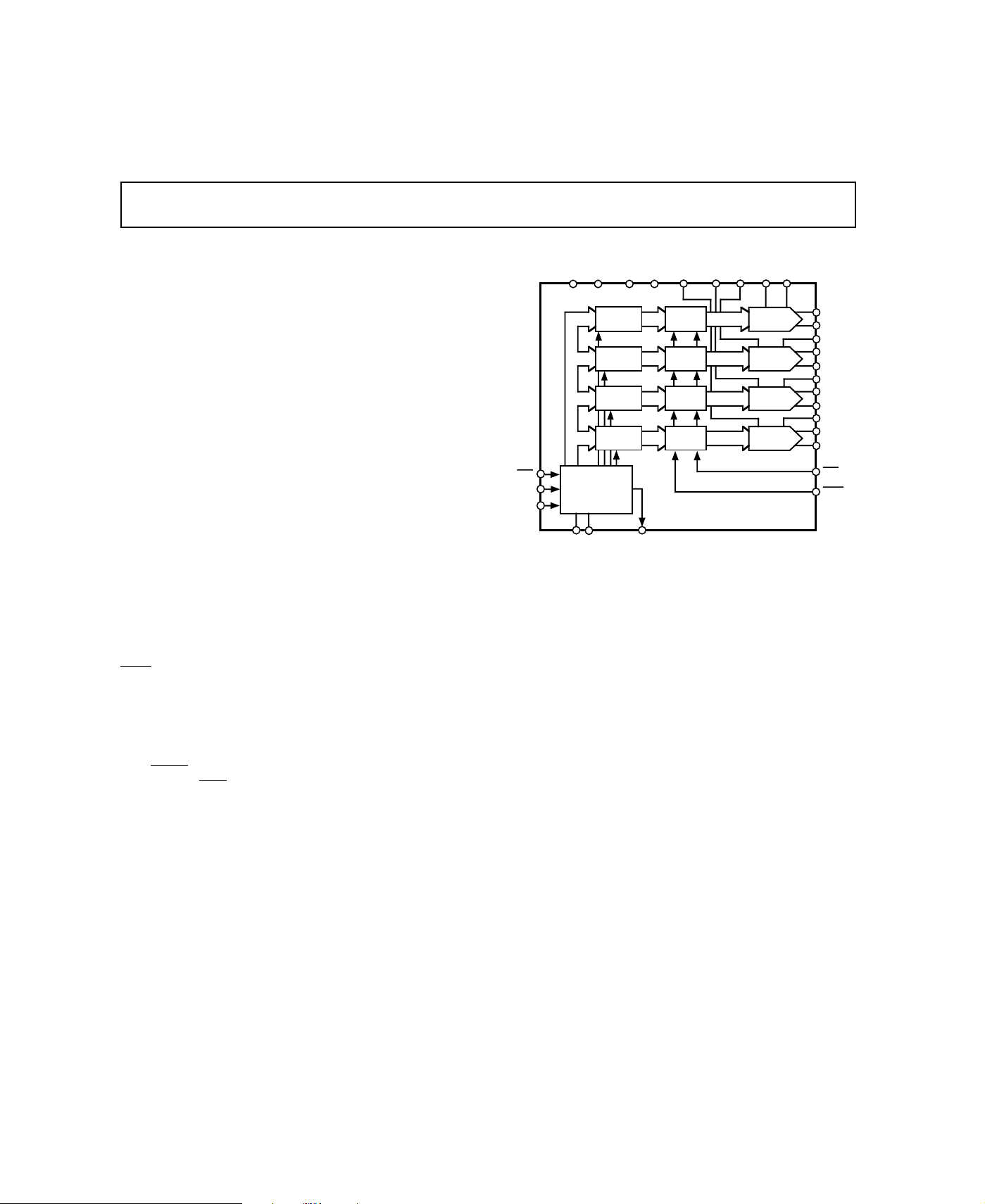
FSIN
CLKIN
SDIN
AD7564
FUNCTIONAL BLOCK DIAGRAM
VDDDGND
AGND
NC
INPUT
LATCH A
INPUT
LATCH B
INPUT
LATCH C
INPUT
LATCH D
12
CONTROL LOGIC
+
INPUT SHIFT
REGISTER
A0 A1
SDOUT
V D
REF
DAC A
12
LATCH
DAC B
12
LATCH
DAC C
12
LATCH
DAC D
12
LATCH
V C
REF
12
12
12
12
V B
REF
AD7564
V A
REF
DAC A
DAC B
DAC C
DAC D
R A
FB
I A
OUT1
I A
OUT2
R B
FB
I B
OUT1
I B
OUT2
R C
FB
I C
OUT1
I C
OUT2
R D
FB
I D
OUT1
I D
OUT2
CLR
LDAC
GENERAL DESCRIPTION
The AD7564 contains four 12-bit DACs in one monolithic
device. The DACs are standard current output with separate
, I
, I
V
REF
OUT1
and RFB terminals. These DACs operate from
OUT2
a single +3.3 V to +5 V supply.
The AD7564 is a serial input device. Data is loaded using
FSIN, CLKIN and SDIN. Two address pins A0 and A1 set up
a device address, and this feature may be used to simplify device
loading in a multi-DAC environment. Alternatively, A0 and A1
can be ignored and the serial out capability used to configure a
daisy-chained system.
All DACs can be simultaneously updated using the asynchro-
LDAC input, and they can be cleared by asserting the
nous
asynchronous
CLR input.
The device is packaged in 28-pin SOIC, SSOP and DIP
packages.
PRODUCT HIGHLIGHTS
1. The AD7564 contains four 12-bit current output DACs with
separate V
REF
inputs.
2. The AD7564 can be operated from a single +3.3 V to +5 V
supply.
3. Simultaneous update capability and reset function are
available.
4. The AD7564 features a fast, versatile serial interface compatible with modern 3 V and 5 V microprocessors and
microcomputers.
5. Low power, 50 µW at 5 V and 33 µW at 3.3 V.
REV. A
Information furnished by Analog Devices is believed to be accurate and
reliable. However, no responsibility is assumed by Analog Devices for its
use, nor for any infringements of patents or other rights of third parties
which may result from its use. No license is granted by implication or
otherwise under any patent or patent rights of Analog Devices.
One Technology Way, P.O. Box 9106, Norwood. MA 02062-9106, U.S.A.
Tel: 617/329-4700 Fax: 617/326-8703
Page 2

AD7564–SPECIFICATIONS
(V
= +4.75 V to +5.25 V; I
Normal Mode
DD
unless otherwise noted)
Parameter B Grade
ACCURACY
Resolution 12 Bits 1 LSB = V
Relative Accuracy ±0.5 LSB max
Differential Nonlinearity ± 0.5 LSB max All Grades Guaranteed Monotonic Over Temperature
Gain Error
+25°C ±4 LSBs max
to T
T
MIN
MAX
Gain Temperature Coefficient
±5 LSBs max
2
2 ppm FSR/°C typ
5 ppm FSR/°C max
Output Leakage Current
I
OUT1
@ +25°C 10 nA max
T
MIN
to T
MAX
50 nA max
REFERENCE INPUT
Input Resistance 6 kΩ min Typical Input Resistance = 9.5 kΩ
13 kΩ max
Ladder Resistance Mismatch 2 % max Typically 0.6%
DIGITAL INPUTS
, Input High Voltage 2.4 V min
V
INH
, Input Low Voltage 0.8 V max
V
INL
, Input Current ±1 µA max
I
INH
CIN, Input Capacitance
2
10 pF max
OUT1
1
A to I
OUT1
D = I
OUT2
A = I
D = AGND = 0 V; V
OUT2
REF
Units Test Conditions/Comments
/212 = 2.44 mV when V
REF
= +10 V; TA = T
MIN
to T
MAX
REF
,
= 10 V
DIGITAL OUTPUT (SDOUT)
Output Low Voltage (V
) 0.4 V max Load Circuit as in Figure 2.
OL
Output High Voltage (VOH) 4.0 V min
POWER REQUIREMENTS
Range 4.75/5.25 V min/V max Part Functions from 3.3 V to 5.25 V
V
DD
Power Supply Rejection
∆Gain/∆V
I
DD
DD
2
–75 dB typ
10 µA max V
= VDD, V
INH
INL
= 0 V
At Input Levels of 0.8 V and 2.4 V, I
Typically 2 mA.
NOTES
1
Temperature range is as follows: B Version: –40°C to +85°C.
2
Not production tested. Guaranteed by characterization at initial product release.
Specifications subject to change without notice.
DD
is
–2–
REV. A
Page 3

(V
Biased Mode
= +3 V to +5.5 V; V
DD
1
, unless otherwise noted)
T
MAX
IOUT1
= V
= 1.23 V; AGND = 0 V; V
IOUT2
Parameter A Grade
= 0 V to 2.45 V; TA = T
REF
2
Units Test Conditions/Comments
MIN
to
AD7564
ACCURACY
Resolution 12 Bits 1 LSB = (V
V
IOUT2
– V
IOUT2
= 1.23 V and V
REF
)/2
REF
12
= 0 V
= 300 µV when
Relative Accuracy ±1 LSB max
Differential Nonlinearity ±0.9 LSB max All Grades Guaranteed Monotonic Over
Temperature
Gain Error
+25°C ±4 LSBs max
to T
T
MIN
Gain Temperature Coefficient
MAX
3
±5 LSBs max
2 ppm FSR/°C typ
5 ppm FSR/°C max
Output Leakage Current See Terminology Section
I
OUT1
@ +25°C 10 nA max
T
MIN
to T
MAX
50 nA max
Input Resistance
@ I
Pins 6 kΩ min This Varies with DAC Input Code
OUT2
DIGITAL INPUTS
, Input High Voltage @ VDD = +5 V 2.4 V min
V
INH
, Input High Voltage @ VDD = +3.3 V 2.1 V min
V
INH
, Input Low Voltage @ VDD = +5 V 0.8 V max
V
INL
, Input Low Voltage @ VDD = +3.3 V 0.6 V max
V
INL
, Input Current ±1 µA max
I
INH
CIN, Input Capacitance
3
10 pF max
DIGITAL OUTPUT (SDOUT) Load Circuit as in Figure 2.
Output Low Voltage (V
Output Low Voltage (V
Output High Voltage (V
Output High Voltage (VOH)V
) 0.4 V max VDD = +5 V
OL
) 0.2 V max VDD = +3.3 V
OL
) 4.0 V min VDD = +5 V
OH
– 0.2 V min VDD = +3.3 V
DD
POWER REQUIREMENTS
Range 3/5.5 V min/V max
V
DD
Power Supply Sensitivity
∆Gain/∆V
I
DD
DD
3
–75 dB typ
10 µA max V
= VDD – 0.1 V min, V
INH
= 0.1 V max;
INL
SDOUT Open Circuit
is typically 2 mA with VDD = +5 V,
I
DD
= 2.4 V min, V
V
INH
= 0.8 V max;
INL
SDOUT Open Circuit
NOTES
1
These specifications apply with the devices biased up at 1.23 V for single supply applications. The model numbering reflects this by means of a "-B" suffix
(for example: AD7564AR-B). Figure 19 is an example of Biased Mode Operation.
2
Temperature ranges is as follows: A Version: –40°C to +85°C.
3
Not production tested. Guaranteed by characterization at initial product release.
Specifications subject to change without notice.
REV. A
–3–
Page 4
AD7564
AC Performance Characteristics
(VDD = +4.75 V to +5.25 V; V
= T
to T
, unless otherwise noted. These characteristics are included for Design Guidance and are
MAX
Normal Mode
AD843; T
A
MIN
not subject to test.)
Parameter B Grade Units Test Conditions/Comments
DYNAMIC PERFORMANCE
Output Voltage Settling Time 550 ns typ To 0.01% of Full-Scale Range. DAC Latch Alternately Loaded
Digital-to-Analog Glitch Impulse 35 nV-s typ Measured with V
Multiplying Feedthrough Error –70 dB max V
Output Capacitance 60 pF max All 1s Loaded to DAC
30 pF max All 0s Loaded to DAC
Channel-to-Channel Isolation –76 dB typ Feedthrough from Any One Reference to the Others with
Digital Crosstalk 5 nV-s typ Effect of All 0s to All 1s Code Transition on Nonselected DACs
Digital Feedthrough 5 nV-s typ Feedthrough to Any DAC Output with
Total Harmonic Distortion –83 dB typ V
Output Noise Spectral Density
@ 1 kHz 30 nV/√
= V
IOUT1
= AGND = 0 V. V
IOUT2
= 6 V rms, 1 kHz sine wave; DAC output op amp is
REF
with All 0s and All 1s
with All 0s and All 1s
REF
= 20 V p-p, 10 kHz Sine Wave. DAC Latch Loaded
REF
with All 0s
20 V p-p, 10 kHz Sine Wave Applied
Wave Applied to SDIN and SCLK
= 6 V rms, 1 kHz Sine Wave
REF
Hz typ All 1s Loaded to the DAC. V
ADOP07
= 0 V. DAC Register Alternately Loaded
FSIN High and Square
= 0 V. Output Op Amp Is
REF
AC Performance Characteristics
(VDD = +3 V to +5.5 V; V
output op amp is AD820; T
Biased Mode
Guidance and are not subject to test.)
Parameter A Grade Units Test Conditions/Comments
DYNAMIC PERFORMANCE
Output Voltage Settling Time 3.5 µs typ To 0.01% of Full-Scale Range. V
Digital to Analog Glitch Impulse 35 nV-s typ Measured with V
Multiplying Feedthrough Error –70 dB max DAC Latch Loaded with all 0s.
Output Capacitance 100 pF max All 1s Loaded to DAC
40 pF max All 0s Loaded to DAC
Digital Feedthrough 5 nV-s typ Feedthrough to Any DAC Output with FSIN HIGH and a Square
Total Harmonic Distortion –76 dB typ
Output Noise Spectral Density
@ 1 kHz 20 nV/√Hz typ All 1s Loaded to DAC. V
IOUT1
= T
A
= V
= 1.23 V; AGND = 0 V. V
IOUT2
to T
MIN
, unless otherwise noted. These characteristics are included for Design
MAX
= 1 kHz, 2.45 V p-p, sine wave biased at 1.23 V; DAC
REF
= 0 V. DAC Latch Alter-
REF
nately Loaded with all 0s and all 1s.
= 0 V and V
IOUT2
REF
nately Loaded with all 0s and all 1s.
Wave Applied to SDIN and CLKIN
= 0 V; V
IOUT2
= 0 V. DAC Register Alter-
= 0 V
REF
–4–
REV. A
Page 5
AD7564
Timing Specifications
1
(TA = T
MIN
to T
unless otherwise noted)
MAX
Limit at Limit at
Parameter V
t
1
t
2
t
3
t
4
t
5
t
6
t
7
2
t
8
t
9
NOTES
1
Not production tested. Guaranteed by characterization at initial product release. All input signals are specified with tr = tf = 5 ns (10% to 90% of VDD) and timed
from a voltage level of 1.6 V for a V
2
t8 is measured with the load circuit of Figure 2 and defined as the time required for the output to cross 0.8 V or 2.4 V with a V
of 3.3 V.
CLKIN(I)
FSIN(I)
SDIN(I)
= +3 V to +3.6 V VDD = +4.75 V to +5.25 V Units Description
DD
180 100 ns min CLKIN Cycle Time
80 40 ns min CLKIN High Time
80 40 ns min CLKIN Low Time
50 30 ns min FSIN Setup Time
50 30 ns min Data Setup Time
10 5 ns min Data Hold Time
125 90 ns min FSIN Hold Time
100 70 ns max SDOUT Valid After CLKIN Falling Edge
80 40 ns min LDAC, CLR Pulse Width
of 5 V and from a voltage level 1.35 V for a VDD of 3.3 V.
DD
t
5
DB15
t
1
t
t
t
4
t
6
2
3
DB0
t
7
of 5 V and 0.6 V or 2.1 V for a V
DD
3
DD
SDOUT(O)
LDAC, CLR
t
8
DB15
t
9
Figure 1. Timing Diagram
I
OL
+1.6V
I
OH
TO OUTPUT
PIN
C
L
50pF
1.6mA
200µA
Figure 2. Load Circuit for Digital Output Timing Specifications
DB0
REV. A
–5–
Page 6

AD7564
NC = NO CONNECT
DGND
I
OUT2
C
I
OUT2
B
AGND
R
FB
C
V
REF
C
I
OUT2
D
RFBB
V
REF
B
I
OUT2
A
V
DD
I
OUT1
C
NC
I
OUT1
B
I
OUT1
D I
OUT1
A
R
FB
D RFBA
V
REF
D V
REF
A
SDOUT
A0
CLR A1
LDAC OCLKIN
FSIN SDIN
13
18
1
2
28
27
5
6
7
24
23
22
3
4
26
25
821
920
10 19
1111
12 17
16
14 15
TOP VIEW
(Not to Scale)
AD7564
ABSOLUTE MAXIMUM RATINGS
1
(TA = +25°C unless otherwise noted)
VDD to DGND . . . . . . . . . . . . . . . . . . . . . . . . . . –0.3 V to +6 V
to DGND . . . . . . . . . . . . . . . . . . . –0.3 V to VDD + 0.3 V
I
OUT1
to DGND . . . . . . . . . . . . . . . . . . . –0.3 V to VDD + 0.3 V
I
OUT2
AGND to DGND . . . . . . . . . . . . . . . . . –0.3 V to V
Digital Input Voltage to DGND . . . . . . –0.3 V to V
, V
V
RFB
Input Current to Any Pin Except Supplies
to DGND . . . . . . . . . . . . . . . . . . . . . . . . . . .±15 V
REF
2
. . . . . . . . ±10 mA
+ 0.3 V
DD
+ 0.3 V
DD
Operating Temperature Range
Commercial Plastic (A, B Versions). . . . . .–40°C to +85°C
Storage Temperature Range . . . . . . . . . . . . . –65°C to +150°C
Junction Temperature . . . . . . . . . . . . . . . . . . . . . . . . . +150°C
DIP Package, Power Dissipation . . . . . . . . . . . . . . . . .875 mW
Thermal Impedance . . . . . . . . . . . . . . . . . . . . 75°C/W
θ
JA
Lead Temperature, Soldering (10 sec) . . . . . . . . . . 260°C
SOIC Package, Power Dissipation . . . . . . . . . . . . . . . . 875 mW
Thermal Impedance . . . . . . . . . . . . . . . . . . . . 75°C/W
θ
JA
Lead Temperature, Soldering (10 sec) . . . . . . . . . . 260°C
Vapor Phase (60 sec) . . . . . . . . . . . . . . . . . . . . . +215°C
Infrared (15 sec) . . . . . . . . . . . . . . . . . . . . . . . . +220°C
SSOP Package, Power Dissipation . . . . . . . . . . . . . . . . 900 mW
Thermal Impedance . . . . . . . . . . . . . . . . . . . 100°C/W
θ
JA
Lead Temperature, Soldering
Vapor Phase (60 sec) . . . . . . . . . . . . . . . . . . . . . +215°C
Infrared (15 sec) . . . . . . . . . . . . . . . . . . . . . . . . +220°C
PIN CONFIGURATION
DIP, SOIC and SSOP Packages
NOTES
1
Stresses above those listed under “Absolute Maximum Ratings” may cause
permanent damage to the device. This is a stress rating only and functional
operation of the device at these or any other conditions above those listed in the
operational sections of this specification is not implied. Exposure to absolute
maximum rating conditions for extended periods may affect device reliability.
2
Transient currents of up to 100 mA will not cause SCR latch-up.
CAUTION
ESD (electrostatic discharge) sensitive device. Electrostatic charges as high as 4000 V readily
accumulate on the human body and test equipment and can discharge without detection.
Although the AD7564 features proprietary ESD protection circuitry, permanent damage may
occur on devices subjected to high energy electrostatic discharges. Therefore, proper ESD
precautions are recommended to avoid performance degradation or loss of functionality.
WARNING!
ESD SENSITIVE DEVICE
ORDERING GUIDE
Temperature Linearity Nominal Package
Model Range Error (LSBs) Supply Voltage Option*
AD7564BN –40°C to +85°C ±0.5 +5 V N-28
AD7564BR –40°C to +85°C ±0.5 +5 V R-28
AD7564BRS –40°C to +85°C ±0.5 +5 V RS-28
AD7564AR-B –40°C to +85°C ±1 +3.3 V to +5 V R-28
AD7564ARS-B –40°C to +85°C ±1 +3.3 V to +5 V RS-28
*N = DIP; R = SOIC; RS = SSOP.
–6–
REV. A
Page 7

AD7564
PIN DESCRIPTIONS
Pin
Number Mnemonic Description
1 DGND Digital Ground.
2I
3V
4I
5R
6V
7I
8I
9R
10 V
11 SDOUT This shift register output allows multiple devices to be connected in a daisy chain configuration.
12
13
14
15 SDIN Serial data input. The device accepts a 16-bit word. DB0 and DB1 are DAC select bits. DB2 and
16 CLKIN Clock Input. Data is clocked into the input shift register on the falling edges of CLKIN.
17 A1 Device address pin. This input in association with A0 gives the device an address. If DB2 and DB3
18 A0 Device address pin. This input in association with A1 gives the device an address.
19 V
20 RFBA Feedback resistor for DAC A.
21 I
22 I
23 V
24 R
25 I
26 N/C No Connect pin.
27 AGND This pin connects to the back gates of the current steering switches. It should be connected to the
28 I
CI
OUT2
DD
CI
OUT1
C Feedback resistor for DAC C.
FB
C DAC C reference input.
REF
DI
OUT2
DI
OUT1
D Feedback resistor for DAC D.
FB
D DAC D reference input.
REF
terminal for DAC C. This should normally connect to the signal ground of the system.
OUT2
Positive power supply. This is +5 V ± 5%.
terminal for DAC C.
OUT1
terminal for DAC D. This should normally connect to the signal ground of the system.
OUT2
terminal for DAC D.
OUT1
CLR Asynchronous CLR input. When this input is taken low, all DAC latches are loaded with all 0s.
LDAC Asynchronous LDAC input. When this input is taken low, all DAC latches are simultaneously
updated with the contents of the input latches.
FSIN Level-triggered control input (active low). This is the frame synchronization signal for the input data.
When
FSIN goes low, it enables the input shift register, and data is transferred on the falling edges of
CLKIN. If the address bits are valid, the 12-bit DAC data is transferred to the appropriate input
latch on the sixteenth falling edge after
FSIN goes low.
DB3 are device address bits. DB4 to DB15 contain the 12-bit data to be loaded to the selected
DAC.
of the serial input stream do not correspond to this address, the data which follows is ignored and
not loaded to any input latch. However, it will appear at SDOUT irrespective of this.
A DAC A reference input.
REF
AI
OUT1
AI
OUT2
B DAC B reference input.
REF
B Feedback resistor for DAC B.
FB
BI
OUT1
terminal for DAC A.
OUT1
terminal for DAC A. This should normally connect to the signal ground of the system.
OUT2
terminal for DAC B.
OUT1
signal ground of the system.
BI
OUT2
terminal for DAC B. This should normally connect to the signal ground of the system.
OUT2
3
REV. A
–7–
Page 8

AD7564
TERMINOLOGY
Relative Accuracy
Relative accuracy or endpoint linearity is a measure of the
maximum deviation from a straight line passing through the
endpoints of the DAC transfer function. It is measured after adjusting for zero error and full-scale error and is normally expressed in Least Significant Bits or as a percentage of full-scale
reading.
Differential Nonlinearity
Differential nonlinearity is the difference between the measured
change and the ideal 1 LSB change between any two adjacent
codes. A specified differential nonlinearity of 1 LSB maximum
ensures monotonicity.
Gain Error
Gain error is a measure of the output error between an ideal
DAC and the actual device output. It is measured with all 1s
in the DAC after offset error has been adjusted out and is expressed in Least Significant Bits. Gain error is adjustable to
zero with an external potentiometer.
Output Leakage Current
Output leakage current is current which flows in the DAC
ladder switches when these are turned off. For the I
terminal, it can be measured by loading all 0s to the DAC and
be measured by loading all 0s to the DAC and measuring the I
current. Minimum current will flow in the I
DAC is loaded with all 1s. This is a combination of the switch
leakage current and the ladder termination resistor current.
The I
Output Capacitance
This is the capacitance from the I
leakage current is typically equal to that in I
OUT2
pin to AGND.
OUT1
OUT1
line when the
OUT2
OUT1
OUT1
.
Output Voltage Settling Time
This is the amount of time it takes for the output to settle to a
specified level for a full-scale input change. For the AD7564, it
is specified with the AD843 as the output op amp.
Digital to Analog Glitch Impulse
This is the amount of charge injected into the analog output
when the inputs change state. It is normally specified as the
area of the glitch in either pA-secs or nV-secs, depending upon
whether the glitch is measured as a current or voltage signal. It
is measured with the reference input connected to AGND and
the digital inputs toggled between all 1s and all 0s.
AC Feedthrough Error
This is the error due to capacitive feedthrough from the DAC
reference input to the DAC I
terminal, when all 0s are
OUT
loaded in the DAC.
Channel-to-Channel Isolation
Channel-to-channel isolation refers to the proportion of input
signal from one DAC’s reference input which appears at the
output of any other DAC in the device and is expressed in dBs.
Digital Crosstalk
The glitch impulse transferred to the output of one converter
due to a change in digital input code to the other converter is
defined as the Digital Crosstalk and is specified in nV-secs.
Digital Feedthrough
When the device is not selected, high frequency logic activity on
the device digital inputs is capacitively coupled through the device to show up at on the I
pin and subsequently on the op
OUT
amp output. This noise is digital feedthrough.
Table I. AD7564 Loading Sequence
DB15 DB0
DB11 DB10 DB9 DB8 DB7 DB6 DB5 DB4 DB3 DB2 DB1 DB0 A1 A0 DS1 DS0
Table II. DAC Selection
DS1 DS0 Function
0 0 DAC A Selected
0 1 DAC B Selected
1 0 DAC C Selected
1 1 DAC D Selected
–8–
REV. A
Page 9

0.5
0.5
0.0
10
0.3
0.1
4
0.2
2
0.4
8
6
V
REF
– Volts
INL – LSBs
NORMAL MODE OF OPERATION
V
DD
= +5V
T
A
= +25°C
0
–10
–90
–60
–70
–80
–50
–40
–30
–20
10
3
10
4
10
6
10
5
FREQUENCY – Hz
V
OUT
B/V
OUT
C – dBs
V
REF
B = 0V
ALL OTHER REFERENCE INPUTS = 20V p-p SINE WAVE
DAC B LOADED WITH ALL 0s
ALL OTHER DACs LOADED WITH ALL 1s
NORMAL MODE OF OPERATION
V
= +5V
DD
T
= +25°C
A
0.4
0.3
DNL – LSBs
0.2
0.1
Typical Performance Curves–AD7564
0.0
2
4
Figure 3. Differential Nonlinearity Error vs. V
6
– Volts
V
REF
8
10
REF
(Normal Mode)
0
V
C = 20V p-p SINE WAVE
REF
–10
ALL OTHER REFERENCE INPUTS = 0V
DAC C LOADED WITH ALL 1s
ALL OTHER DACs LOADED WITH ALL 0s
–20
–30
–40
C – dBs
OUT
–50
B/V
–60
OUT
V
–70
–80
–90
3
10
4
10
FREQUENCY – Hz
5
10
6
10
Figure 4. Channel-to-Channel Isolation (1 DAC to 1 DAC)
Figure 6. Integral Nonlinearity Error vs. V
REF
(Normal Mode)
Figure 7. Channel-to-Channel Isolation (1 DAC to All
Other DACs)
–50
–60
–70
THD – dBs
–80
–90
–100
2
10
Figure 5. Total Harmonic Distortion vs. Frequency
(Normal Mode)
REV. A
NORMAL MODE OF OPERATION
V
= +5V
DD
V
= +6V rms
IN
OP AMP = AD713
T
= +25°C
A
3
10
FREQUENCY – Hz
0
VDD = +5V
–10
T
= +25°C
A
V
= 20V p-p
–20
IN
OP AMP = AD711
–30
–40
–50
GAIN – dB
–100
4
10
5
10
DAC LOADED WITH ALL 0s
–60
–70
–80
–90
1k
10k 100k 1M 10M
DAC LOADED WITH ALL 1s
FREQUENCY – Hz
Figure 8. Multiplying Frequency Response vs. Digital
Code (Normal Mode)
–9–
Page 10

AD7564
2.0
BIAS
| – Volts
VDD = +3.3V
T
= +25°C
A
OP AMP = AD820
V
= +1.23V (AD589)
REF
1.21.00.80.6
1.8
1.6
1.4
1.2
1.0
INL – LSBs
0.8
0.6
0.4
0.2
0.0
0.2
0.4
|V
– V
REF
Figure 9. Integral Nonlinearity Error vs. V
(Biased Mode)
2.0
BIAS
| – Volts
VDD = +5V
T
= +25°C
A
OP AMP = AD820
V
= +1.23V (AD589)
BIAS
1.21.00.80.6
1.8
1.6
1.4
1.2
1.0
INL – LSBs
0.8
0.6
0.4
0.2
0.0
0.2
0.4
|V
– V
REF
REF
1.4
1.4
2.0
– V
BIAS
VDD = +3.3V
T
= +25°C
A
OP AMP = AD820
V
= +1.23V (AD589)
REF
| – Volts
1.21.00.80.6
1.8
1.6
1.4
1.2
1.0
0.8
DNL – LSBs
0.6
0.4
0.2
0.0
0.2
0.4
|V
REF
Figure 12. Differential Nonlinearity Error vs. V
(Biased Mode)
2.0
– V
BIAS
VDD = +5V
T
= +25°C
A
OP AMP = AD820
V
= +1.23V (AD589)
BIAS
| – Volts
1.21.00.80.6
1.8
1.6
1.4
1.2
1.0
0.8
DNL – LSBs
0.6
0.4
0.2
0.0
0.2
0.4
|V
REF
1.4
REF
1.4
Figure 10. Integral Nonlinearity Error vs. V
REF
(Biased Mode)
0.2
0.1
0.0
–0.1
–0.2
–0.3
LINEARITY ERROR – LSBs
–0.4
–0.5
0
1024
VDD = +3.3V
T
= +25°C
A
V
= 1.23V
BIAS
V
= 0V
REF
CODE – LSBs
30722048
4095
Figure 11. All Codes Linearity Plot (Biased Mode)
Figure 13. Differential Nonlinearity Error vs. V
REF
(Biased Mode)
0.4
NORMAL MODE
V
= +5V
DD
T
= +25°C
A
V
= 10V
0.3
REF
0.2
0.1
LINEARITY ERROR – LSBs
0.0
–0.1
CODE – LSBs
409510240 30722048
Figure 14. All Codes Linearity Plot (Normal Mode)
–10–
REV. A
Page 11

AD7564
16-BIT INPUT
SHIFT REGISTER
CLKIN
FSIN
SDIN
SDOUT
GENERAL DESCRIPTION
D/A Section
The AD7564 contains four 12-bit current output D/A converters. A simplified circuit diagram for one of the D/A converters
is shown in Figure 15.
V
REF
2R 2R 2R 2R 2R 2R 2R
CBA
R
R
S9
SHOWN FOR ALL 1s ON DAC
S8 S0
R
R/2
R
I
I
OUT2
FB
OUT1
Figure 15. Simplified D/A Circuit Diagram
A segmented scheme is used whereby the 2 MSBs of the 12-bit
data word are decoded to drive the three switches A, B and C.
The remaining 10 bits of the data word drive the switches S0 to
S9 in a standard R-2R ladder configuration.
Each of the switches A to C steers 1/4 of the total reference
current with the remaining current passing through the R-2R
section.
All DACs have separate V
REF
OUT1
OUT2
and R
FB
pins.
, I
, I
When an output amplifier is connected in the standard configuration of Figure 17, the output voltage is given by:
Bringing the
CLR line low resets the DAC latches to all 0s. The
input latches are not affected so that the user can revert to the
previous analog output if desired.
Figure 16. Input Logic
UNIPOLAR BINARY OPERATION
(2-Quadrant Multiplication)
Figure 17 shows the standard unipolar binary connection diagram for one of the DACs in the AD7564. When V
is an ac
IN
signal, the circuit performs 2-quadrant multiplication. Resistors
R1 and R2 allow the user to adjust the DAC gain error. Offset
can be removed by adjusting the output amplifier offset voltage.
R2 10Ω
A
R
R1 20Ω
V
IN
V
A
REF
NOTES
1. ONLY ONE DAC IS SHOWN FOR CLARITY.
2. DIGITAL INPUT CONNECTIONS ARE OMITTED.
3. C1 PHASE COMPENSATION (5–15pF) MAY BE
REQUIRED WHEN USING HIGH SPEED AMPLIFIER.
FB
DAC A
AD7564
I
OUT1
I
OUT2
SIGNAL
A
A
GND
C1
A1
A1: AD707
AD711
AD843
AD845
V
OUT
3
V
= D ×V
OUT
REF
where D is the fractional representation of the digital word
loaded to the DAC. Thus, in the AD7564, D can be set from 0
to 4095/4096.
Interface Section
The AD7564 is a serial input device. Three input signals control the serial interface. These are
FSIN, CLKIN and SDIN.
The timing diagram is shown in Figure 1.
Data applied to the SDIN pin is clocked into the input shift reg-
ister on each falling edge of CLKIN. SDOUT is the shift register output. It allows multiple devices to be connected in a daisy
chain fashion with the SDOUT pin of one device connected to
the SDIN of the next device.
FSIN is the frame synchronization
for the device.
When the sixteen bits have been received in the input shift regis-
ter, DB2 and DB3 (A0 and A1) are checked to see if they correspond to the state on pins A0 and A1. If it does, then the word
is accepted. Otherwise, it is disregarded. This allows the user
to address a number of AD7564s in a very simple fashion. DB1
and DB0 of the 16-bit word determine which of the four DAC
input latches is to be loaded. When the
LDAC line goes low, all
four DAC latches in the device are simultaneously loaded with
the contents of their respective input latches and the outputs
change accordingly.
Figure 17. Unipolar Binary Operation
A1 should be chosen to suit the application. For example, the
AD707 is ideal for very low bandwidth applications while the
AD843 and AD845 offer very fast settling time in wide bandwidth applications. Appropriate multiple versions of these amplifiers can be used with the AD7564 to reduce board space
requirements.
The code table for Figure 17 is shown in Table III.
Table III. Unipolar Binary Code Table
Digital Input Analog Output
MSB . . . LSB (V
1111 1111 1111 –V
1000 0000 0001 –V
1000 0000 0000 –V
0111 1111 1111 –V
0000 0000 0001 –V
0000 0000 0000 –V
NOTE
Nominal LSB size for the circuit of Figure 17 is given by: V
as Shown in Figure 17)
OUT
(4095/4096)
REF
(2049/4096)
REF
(2048/4096)
REF
(2047/4096)
REF
(1/4096)
REF
(0/4096) = 0
REF
(1/4096).
REF
REV. A
–11–
Page 12

AD7564
A1
V
REF
A
RFBA
I
OUT1
A
V
IN
V
OUT
I
OUT2
A
R1 R2
AD7564
DAC A
1. ONLY ONE DAC IS SHOWN FOR CLARITY.
2. DIGITAL INPUT CONNECTIONS ARE OMITTED.
3. C1 PHASE COMPENSATION (5–15pF) MAY BE
REQUIRED WHEN USING HIGH SPEED AMPLIFIER.
NOTES
BIPOLAR OPERATION
4-Quadrant Multiplication)
Figure 18 shows the standard connection diagram for bipolar
operation of any one of the DACs in the AD7564. The coding
is offset binary as shown in Table IV. When V
is an ac signal,
IN
the circuit performs 4-quadrant multiplication. To maintain
the gain error specifications, resistors R3, R4 and R5 should be
ratio matched to 0.01%.
R4 20kΩ
R
R1 20Ω
V
IN
V
REF
NOTES:
1. ONLY ONE DAC IS SHOWN FOR CLARITY.
2. DIGITAL INPUT CONNECTIONS ARE OMITTED.
3. C1 PHASE COMPENSATION (5–15pF) MAY BE
REQUIRED WHEN USING HIGH SPEED AMPLIFIER, A1.
DAC A
A
AD7564
R2 10Ω
A
FB
I
OUT1
I
OUT2
SIGNAL
A
A
GND
C1
A1
R3
10kΩ
20kΩ
R5
R4 20Ω
A2
V
OUT
Figure 18. Bipolar Operation (4-Quadrant Multiplication)
Table IV. Bipolar (Offset Binary) Code Table
Digital Input Analog Output
MSB . . . LSB (V
1111 1111 1111 –V
1000 0000 0001 –V
1000 0000 0000 –V
0111 1111 1111 –V
0000 0000 0001 –V
0000 0000 0000 –V
NOTE
Nominal LSB size for the circuit of Figure 18 is given by: V
as Shown in Figure 18)
OUT
(2047/2048)
REF
(1/2048)
REF
(0/2048 = 0)
REF
(1/2048)
REF
(2047/2048)
REF
(2048/2048) = –V
REF
(1/2048).
REF
REF
In the current mode circuit of Figure 19, I
is biased positive by an amount V
. For the circuit to operate
BIAS
and hence I
OUT2
OUT1
,
correctly, the DAC ladder termination resistor must be connected internally to I
. This is the case with the AD7564.
OUT2
The output voltage is given by:
V
OUT
= D ×
R
R
DAC
FB
×(V
BIAS–VIN
+V
)
BIAS
As D varies from 0 to 4095/4096, the output voltage varies
from V
OUT
= V
BIAS
to V
OUT
= 2 V
– VIN. V
BIAS
should be a
BIAS
low impedance source capable of sinking and sourcing all possible variations in current at the I
terminal without any
OUT2
problems.
Voltage Mode Circuit
Figure 20 shows DAC A of the AD7564 operating in the
voltage-switching mode. The reference voltage, V
OUT1
pin, I
to the I
voltage is available at the V
is connected to AGND and the output
OUT2
terminal. In this configuration, a
REF
is applied
IN
positive reference voltage results in a positive output voltage;
making single supply operation possible. The output from the
DAC is a voltage at a constant impedance (the DAC ladder resistance). Thus, an op amp is necessary to buffer the output
voltage. The reference voltage input no longer sees a constant
input impedance, but one which varies with code. So, the voltage input should be driven from a low impedance source.
It is important to note that V
is limited to low voltages be-
IN
cause the switches in the DAC no longer have the same sourcedrain voltage. As a result, their on-resistance differs and this
degrades the integral linearity of the DAC. Also, V
must not
IN
go negative by more than 0.3 volts or an internal diode will turn
on, causing possible damage to the device. This means that the
full-range multiplying capability of the DAC is lost.
SINGLE SUPPLY APPLICATIONS
The “–B” versions of the AD7564 are specified and tested for
single supply applications. Figure 19 shows a typical circuit for
operation with a single +3.3 V to +5 V supply.
V
IN
V
A
REF
V
NOTES:
1. ONLY ONE DAC IS SHOWN FOR CLARITY.
2. DIGITAL INPUT CONNECTIONS ARE OMITTED.
3. C1 PHASE COMPENSATION (5–15pF) MAY BE
REQUIRED WHEN USING HIGH SPEED AMPLIFIER, A1.
Figure 19. Single Supply Current Mode Operation
RFBA
DAC A
AD7564
BIAS
I
I
OUT1
OUT2
A
A1
A
V
OUT
Figure 20. Single Supply Voltage Switching Mode
Operation
–12–
REV. A
Page 13

AD7564
CLR
FSIN
SCLK
SDIN
LDAC
PC5
PC7
SCK
MOSI
PC6
64HC11*
AD7564*
*ADDITIONAL PINS OMMITTED FOR CLARITY
MICROPROCESSOR INTERFACING
AD7564 to 80C51 Interface
A serial interface between the AD7564 and the 80C51 microcontroller is shown in Figure 21. TXD of the 80C51 drives
SCLK of the AD7564 while RXD drives the serial data line of
the part. The FSIN signal is derived from the port line P3.3.
The 80C51 provides the LSB of its SBUF register as the first bit
in the serial data stream. Therefore, the user will have to ensure
that the data in the SBUF register is arranged correctly so that
the data word transmitted to the AD7564 corresponds to the
loading sequence shown in Table I. When data is to be transmitted to the part, P3.3 is taken low. Data on RXD is valid on
the falling edge of TXD. The 80C51 transmits its serial data in
8-bit bytes with only eight falling clock edges occurring in the
transmit cycle. To load data to the AD7564, P3.3 is left low
after the first eight bits are transferred and a second byte of data
is then transferred serially to the AD7564. When the second
serial transfer is complete, the P3.3 line is taken high. Note that
the 80C51 outputs the serial data byte in a format which has the
LSB first. The AD7564 expects the MSB first. The 80C51
transmit routine should take this into account.
AD7564*
80C51*
AD7564 to 68HC11 Interface
Figure 22 shows a serial interface between the AD7564 and the
68HC11 microcontroller. SCK of the 68HC11 drives SCLK of
the AD7564 while the MOSI output drives the serial data line of
the AD7564. The FSIN signal is derived from a port line
(PC7 shown).
For correct operation of this interface, the 68HC11 should be
configured such that its CPOL bit is a 0 and its CPHA bit is a 1.
When data is to be transmitted to the part, PC7 is taken low.
When the 68HC11 is configured like this, data on MOSI is valid
on the falling edge of SCK. The 68HC11 transmits its serial
data in 8-bit bytes (MSB first), with only eight falling clock
edges occurring in the transmit cycle. To load data to the
AD7564 , PC7 is left low after the first eight bits are transferred
and a second byte of data is then transferred serially to the
AD7564. When the second serial transfer is complete, the PC7
line is taken high.
3
P3.5
P3.4
P3.3
TXD
RXD
*ADDITIONAL PINS OMMITTED FOR CLARITY
CLR
LDAC
FSIN
SCLK
SDIN
Figure 21. AD7564 to 80C51 Interface
LDAC and CLR on the AD7564 are also controlled by 80C51
port outputs. The user can bring
LDAC low after every two
bytes have been transmitted to update the DAC which has been
programmed. Alternatively, it is possible to wait until all the input registers have been loaded (sixteen byte transmits) and then
update the DAC outputs.
Figure 22. AD7564 to 64HC11 Interface
In Figure 22, LDAC and CLR are controlled by the PC6
and PC5 port outputs. As with the 80C51, each DAC of the
AD7564 can be updated after each two-byte transfer, or else
all DACs can be simultaneously updated. This interface
is suitable for both 3 V and 5 V versions of the 68HC11
microcontroller.
REV. A
–13–
Page 14

AD7564
AD7564 to ADSP-2101/ADSP-2103 Interface
Figure 23 shows a serial interface between the AD7564 and the
ADSP-2101/ADSP-2103 digital signal processors. The ADSP2101 operates from 5 V while the ADSP-2103 operates from
3 V supplies. These processors are set up to operate in the
SPORT Transmit Alternate Framing Mode.
The following DSP conditions are recommended: Internal
SCLK; Active low Framing Signal; 16-bit word length. Transmission is initiated by writing a word to the TX register after the
SPORT has been enabled. The data is then clocked out on every rising edge of SCLK after TFS goes low. TFS stays low until the next data transfer.
ADSP-2101/
ADSP-2103
FO
TFS
DT
SCLK
*ADDITIONAL PINS OMMITTED FOR CLARITY
+5V
Figure 23. AD7564 to ADSP-2101/ADSP-2103 Interface
AD7564 to TMS320C25 Interface
Figure 24 shows an interface circuit for the TMS320C25 digital
signal processor. The data on the DX pin is clocked out of
the processor’s Transmit Shift Register by the CLKX signal.
Sixteen-bit transmit format should be chosen by setting the FO
bit in the ST1 register to 0. The transmit operation begins
when data is written into the data transmit register of the
TMS320C25. This data will be transmitted when the FSX line
goes low while CLKX is high or going high. The data, starting
with the MSB, is then shifted out to the DX pin on the rising
edge of CLKX. When all bits have been transmitted, the user
can update the DAC outputs by bringing the XF output flag
low.
AD7564*
CLR
LDAC
FSIN
SDIN
CLKIN
TMS320C25*
XF
FSX
DX
CLKX
GENERATION
*ADDITIONAL PINS OMMITTED FOR CLARITY
+5V
CLOCK
AD7564*
CLR
LDAC
FSIN
SDIN
CLKIN
Figure 24. AD7564 to TMS320C25 Interface
APPLICATION HINTS
Output Offset
CMOS D/A converters in circuits such as Figures 17, 18 and 19
exhibit a code dependent output resistance which in turn can
cause a code dependent error voltage at the output of the amplifier. The maximum amplitude of this error, which adds to the
D/A converter nonlinearity, depends on V
, where VOS is the
OS
amplifier input offset voltage. For the AD7564 to maintain
specified accuracy with V
be no greater than 500 µV, or (50 × 10–6) × (V
V
OS
at 10 V, it is recommended that
REF
REF
), over
the temperature range of operation. Suitable amplifiers include
the ADOP-07, ADOP-27, AD711, AD845 or multiple versions
of these.
Temperature Coefficients
The gain temperature coefficient of the AD7564 has a maximum value of 5 ppm/°C and a typical value of 2 ppm/°C. This
corresponds to gain shifts of 2 LSBs and 0.8 LSBs respectively
over a 100°C temperature range. When trim resistors R1 and
R2 are used to adjust full scale in Figures 17 and 18, their temperature coefficients should be taken into account. For further
information see “Gain Error and Gain Temperature Coefficient
of CMOS Multiplying DACs,” Application Note, Publication
Number E630c-5-3/86, available from Analog Devices.
High Frequency Considerations
The output capacitances of the AD7564 DACs work in conjunction with the amplifier feedback resistance to add a pole to
the open loop response. This can cause ringing or oscillation.
Stability can be restored by adding a phase compensation capacitor in parallel with the feedback resistor. This is shown as
C1 in Figures 17 and 18.
–14–
REV. A
Page 15

AD7564
APPLICATIONS
Programmable State Variable Filter
The AD7564 with its multiplying capability and fast settling
time is ideal for many types of signal conditioning applications.
The circuit of Figure 25 shows its use in a state variable filter
design. This type of filter has three outputs: low pass, high pass
and bandpass. The particular version shown in Figure 25 uses
the AD7564 to control the critical parameters f
, Q and AO. In-
O
stead of several fixed resistors, the circuit uses the DAC equivalent resistances as circuit elements.
Thus, R1 in Figure 25 is controlled by the 12-bit digital word
loaded to DAC A of the AD7564. This is also the case with R2,
R3 and R4. The fixed resistor R5 is the feedback resistor, R
DAC Equivalent Resistance, R
where: R
is the DAC ladder resistance
LADDER
EQ
= (R
LADDER
× 4096)/N
FB
B.
N is the DAC Digital Code in Decimal (0 < N < 4096)
R8
30kΩ
R6
10kΩ
A1
A2 A3 A4
In the circuit of Figure 25:
C1 = C2, R7 = R8, R3 = R4 (i.e., the same code is loaded to
each DAC).
Resonant Frequency, f
Quality Factor, Q = (R6/R8)
Bandpass Gain, A
= 1/(2 π R3C1)
O
×
(R2/R5)
= –R2/R1
O
Using the values shown in Figure 25, the Q range is 0.3 to 5 and
the f
range is 0 to 12 kHz.
O
C3 10pF
R7
30kΩ
HIGH
PASS
OUTPUT
C1 1000pF C2 1000pF
LOW
PASS
OUTPUT
3
I
AI
OUT1
REF
DAC A
(R1)
A
I
AI
OUT2
V
IN
V
NOTES
1. A1, A2, A3, A4, : 1/4 X AD713.
2. DIGITAL INPUT CONNECTIONS ARE OMITTED.
3. C3 IS A COMPENSATION CAPACITOR TO ELIMINATE Q AND GAIN VARIATIONS
CAUSED BY AMPLIFIER GAIN AND BANDWIDTH LIMITATIONS.
BRFBBV
OUT1
R5
DAC B
(R2)
BI
OUT2
REF
AD7564
CI
B
REF
DAC C
(R3)
AGND
Figure 25. Programmable 2nd Order State Variable Filter
CV
OUT1
REF
DAC D
CI
OUT2
DI
(R4)
OUT2
DV
OUT1
D
BAND
PASS
OUTPUT
REV. A
–15–
Page 16

AD7564
MECHANICAL INFORMATION
Dimensions shown in inches and (mm).
28-Pin DIP (N-28)
0.299 (7.60)
0.291 (7.39)
PIN 1
0.01 (0.254)
0.006 (0.15)
28
1
0.200
(5.080)
MAX
0.020 (0.508)
0.015 (0.381)
LEADS ARE SOLDER DIPPED OR TIN-PLATED ALLOY 42 OR COPPER.
1.450 (36.83)
1.440 (36.576)
0.105 (2.67)
0.095 (2.41)
0.065 (1.65)
0.045 (1.14)
15
14
0.175 (4.45)
0.120 (3.05)
28-Lead SOIC (R-28)
28
1
0.708 (18.02)
0.696 (17.67)
0.050 (1.27)
BSC
1. LEAD NO. 1 IDENTIFIED BY A DOT.
2. SOIC LEADS WILL BE EITHER TIN PLATED OF SOLDER DIPPED
IN ACCORDANCE WITH MIL-M-38510 REQUIREMENTS.
0.019 (0.49)
0.014 (0.35)
15
14
0.550 (13.97)
0.530 (13.462)
0.012 (0.305)
0.008 (0.203)
0.414 (10.52)
0.398 (10.10)
0.096 (2.44)
0.089 (2.26)
0.606 (15.39)
0.594 (15.09)
0.013 (0.32)
0.009 (0.23)
0.03 (0.76)
0.02 (0.51)
0.160 (4.07)
0.140 (3.56)
o
15
o
0
0.042 (1.067)
0.018 (0.457)
C1977–18–10/94
28
PIN 1
0.008 (0.203)
0.002 (0.050)
28-Lead SSOP (RS-28)
15
0.212 (5.38)
0.205 (5.207)
1
0.407 (10.34)
0.397 (10.08)
0.0256 (0.65)
BSC
1. LEAD NO. 1 IDENTIFIED BY A DOT.
2. LEADS WILL BE EITHER TIN PLATED OR SOLDER DIPPED
IN ACCORDANCE WITH MIL-M-38510 REQUIREMENTS
14
0.009 (0.229)
0.005 (0.127)
0.07 (1.78)
0.066 (1.67)
0.311 (7.9)
0.301 (7.64)
8
°
0
°
0.03 (0.762)
0.022 (0.558)
PRINTED IN U.S.A.
–16–
REV. A
 Loading...