

Page 1
LC2MOS
a
FEATURES
Two 12-Bit DACs in One Package
DAC Ladder Resistance Matching: 0.5%
Space Saving Skinny DIP and Surface
Mount Packages
4-Quadrant Multiplication
Low Gain Error (1 LSB max Over Temperature)
Fast Interface Timing
APPLICATIONS
Automatic Test Equipment
Programmable Filters
Audio Applications
Synchro Applications
Process Control
GENERAL DESCRIPTION
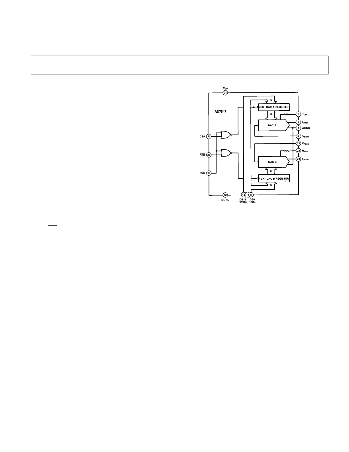
The AD7547 contains two 12-bit current output DACs on one
monolithic chip. Also on-chip are the level shifters, data registers and control logic for easy microprocessor interfacing. There
are 12 data inputs.
loading. Data is latched into the DAC registers on the rising
edge of
processors and accepts TTL, 74HC and 5 V CMOS logic level
inputs.
The D/A converters provide 4-quadrant multiplication capabilities with separate reference inputs and feedback resistors.
Monolithic construction ensures that thermal and gain error
tracking is excellent. 12-bit monotonicity is guaranteed for both
DACs over the full temperature range.
The AD7547 is manufactured using the Linear Compatible
CMOS (LC
precision linear circuitry to be fabricated on the same die.
WR. The device is speed compatible with most micro-
CSA, CSB, WR control DAC selection and
2
MOS) process. This allows fast digital logic and
Parallel Loading Dual 12-Bit DAC
AD7547
FUNCTIONAL BLOCK DIAGRAM
PRODUCT HIGHLIGHTS
1. DAC to DAC Matching
Since both DACs are fabricated on the same chip, precise
matching and tracking is inherent. Many applications which
are not practical using two discrete DACs are now possible.
Typical matching: 0.5%.
2. Small Package Size
The AD7547 is available in 0.3" wide 24-pin DIPs and
SOICs and in 28-terminal surface mount packages.
3. Wide Power Supply Tolerance
The device operates on a +12 V to +15 V V
tolerance on this nominal figure. All specifications are guaranteed over this range.
, with ±10%
DD
REV. A
Information furnished by Analog Devices is believed to be accurate and
reliable. However, no responsibility is assumed by Analog Devices for its
use, nor for any infringements of patents or other rights of third parties
which may result from its use. No license is granted by implication or
otherwise under any patent or patent rights of Analog Devices.
One Technology Way, P.O. Box 9106, Norwood, MA 02062-9106, U.S.A.
Tel: 617/329-4700 Fax: 617/326-8703
Page 2
AD7547–SPECIFICA TIONS
(VDD = +12 V to +15 V, 610%, V
1
O V. All specifications T
MIN
to T
= V
REFA
unless otherwise noted.)
MAX
= 10 V; I
REFB
OUTA
= I
= AGND =
OUTB
Parameter J, A Versions K, B Versions L, C Versions S Version T Version U Version Units Test Conditions/Comments
ACCURACY
Resolution 12 12 12 12 12 12 Bits
Relative Accuracy ±1 ± 1/2 ± 1/2 ± 1 ± 1/2 ±1/2 LSB max
Differential Nonlinearity ± 1 ±1 ±1 ±1 ±1 ± 1 LSB max All grades guaranteed
monotonic over temperature.
Gain Error ±6 ± 3 ± l ±6 ±3 ±2 LSB max Both DAC registers loaded
with all 1s.
Gain Temperature Coefficient2;
∆Gain/∆Temperature ±5 ± 5 ±5 ± 5 ±5 ± 5 ppm/°C max Typical value is 1 ppm/°C
Output Leakage Current
I
OUTA
+25°C 10 10 10 10 10 10 nA max DAC A Register loaded
T
to T
MIN
MIN
to T
MAX
MAX
I
OUTB
+25°C 10 10 10 10 10 10 nA max DAC B Register loaded
T
150 150 150 250 250 250 nA max with all 0s.
150 150 150 250 250 250 nA max with all 0s.
REFERENCE INPUT
Input Resistance 9 9 9 999kΩ min Typical Input Resistance = 14 kΩ
20 20 20 20 20 20 k Ω max
V
, V
REFA
REFB
Input Resistance Match ±3 ± 3 ± 1 ±3 ±3 ±1 % max Typically ±0.5%
DIGITAL INPUTS
VIH (Input High Voltage) 2.4 2.4 2.4 2.4 2.4 2.4 V min
VIL (lnput Low Voltage) 0.8 0.8 0.8 0.8 0.8 0.8 V max
IIN (Input Current)
+25°C ±1 ± 1 ±1 ± 1 ±1 ± 1 µA max VIN = V
T
to T
MIN
CIN (Input Capacitance)
POWER SUPPLY
V
DD
I
DD
MAX
3
±10 ±10 ±10 ±10 ±10 ±10 µA max
2
10 10 10 10 10 10 pF max
10.8/16.5 10.8/16.5 10.8/16.5 10.8/16.5 10.8/16.5 10.8/16.5 V min/V max
2 2 2 2 2 2 mA max
DD
AC PERFORMANCE CHARACTERISTICS
These characteristics are included for Design Guidance only and are not subject to test.
(VDD = +12 V to +15 V; V
Parameter TA = +258CT
Output Current Settling Time 1.5 µs max To 0.01 % of full-scale range. I
Digital-to-Analog Glitch Impulse 7 nV-s typ Measured with V
to I
to I
to I
to I
4
OUTA
OUTB
DD
OUTB
OUTA
AC Feedthrough
V
REFA
V
REFB
Power Supply Rejection
∆Gain/∆V
Output Capacitance
C
OUTA
C
OUTB
C
OUTA
C
OUTB
Channel-to-Channel Isolation
V
REFA
V
REFB
Digital Crosstalk 7 nV-s typ Measured for a Code Transition of all 0s to all 1s.
Output Noise Voltage Density 25 nV/√Hz typ Measured between R
(10 Hz–100 kHz) Frequency of measurement is 10 Hz–100 kHz.
Total Harmonic Distortion –82 dB typ VIN = 6 V rms, 1 kHz. Both DACs loaded with all 1s.
NOTES
1
Temperature range as follows: J, K, L Versions, –40°C to +85°C; A, B, C Versions, –40°C to +85°C; S, T, U Versions, –55 °C to +125°C.
2
Sample tested at +25°C to ensure compliance.
3
Functional at VDD = 5 V with degraded specifications.
4
Pin 12 (DGND) on ceramic DIPs is connected to lid.
Specifications subject to change without notice.
REFA
= V
= +10 V, I
REFB
OUTA
= I
= AGND = 0 V. Output Amplifiers are AD644 except where noted.)
OUTB
= T
A
MIN
, T
MAX
Units Test Conditions/Comments
DAC output measured from rising edge of WR.
Typical Value of Settling Time is 0.8 µs.
= V
load = 100 Ω, C
loaded with all 0s and all 1s.
–70 –65 dB max V
–70 –65 dB max registers loaded with all 0s.
REFA
, V
REFA
= 13 pF. DAC registers alternately
EXT
= 20 V p-p, 10 kHz sine wave. DAC
REFB
±0.01 ±0.02 % per % max ∆VDD = VDD max – VDD min
70 70 pF max DAC A, DAC B loaded with all 0s.
70 70 pF max
140 140 pF max DAC A, DAC B loaded with all 1s.
140 140 pF max
–84 dB typ V
–84 dB typ V
= 20 V p-p 10 kHz sine wave, V
REFA
Both DACs loaded with all 1s.
= 20 V p-p 10 kHz sine wave, V
REFB
Both DACs loaded with all 1s.
I
, I
OUTA
Load = 100 Ω, C
OUTB
FBA
–2–
REFB
and I
load = 100 Ω, C
OUT
= 0 V. I
OUTA
REFB
REFA
= 13 pF
EXT
or R
OUTA
FBB
, I
OUTB
= 0 V.
= 0 V.
and I
OUTB
EXT
.
= 13 pF.
REV. A
Page 3
AD7547
WARNING!
ESD SENSITIVE DEVICE
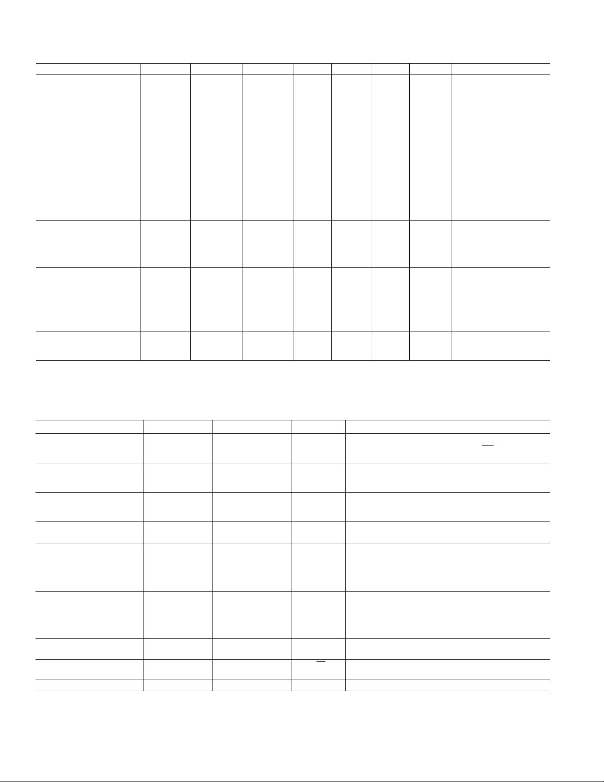
TIMING CHARACTERISTICS
(VDD = 10.8 V to 16.5 V, V
REFA
= V
= +10 V, I
REFB
OUTA
= I
OUTB
= AGND = 0 V)
Limit at Limit at
Limit at T
= –408CT
A
= –558C
A
Parameter TA = +258C to +858C to +1258C Units Test Conditions/Comments
t
1
t
2
t
3
t
4
t
5
Specifications subject to change without notice.
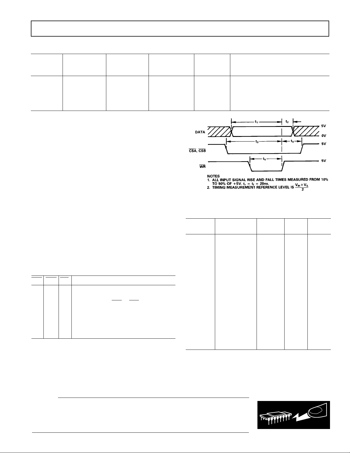
60 80 80 ns min Data Setup Time
25 25 25 ns min Data Hold Time
80 80 100 ns min Chip Select to Write Setup Time
0 0 0 ns min Chip Select to Write Hold Time
80 80 100 ns min Write Pulse Width
ABSOLUTE MAXIMUM RATINGS*
(TA = +25°C unless otherwise noted)
VDD to DGND . . . . . . . . . . . . . . . . . . . . . . . . . .–0.3 V, +17 V
V
, V
REFA
V
RFBA
Digital Input Voltage to DGND . . . . . . . –0.3 V, V
I
OUTA
AGND to DGND . . . . . . . . . . . . . . . . . . –0.3 V, V
to AGND . . . . . . . . . . . . . . . . . . . . . . . . .±25 V
REFB
, V
to AGND . . . . . . . . . . . . . . . . . . . . . . . . . ±25 V
RFBB
, I
to DGND . . . . . . . . . . . . . . –0.3 V, VDD +0.3 V
OUTB
+0.3 V
DD
+0.3 V
DD
Power Dissipation (Any Package)
To +75°C . . . . . . . . . . . . . . . . . . . . . . . . . . . . . . . . 450 mW
Derates above +75°C . . . . . . . . . . . . . . . . . . . . . . 6 mW/°C
Operating Temperature Range
Commercial Plastic (J, K, L Versions) . . . . –40°C to +85°C
Industrial Hermetic (A, B, C Versions) . . . –40°C to +85°C
Extended Hermetic (S, T, U Versions) . . . –55°C to +125°C
Storage Temperature . . . . . . . . . . . . . . . . –65°C to +150°C
Lead Temperature (Soldering, 10 secs) . . . . . . . . . . . +300°C
*Stresses above those listed under “Absolute Maximum Ratings” may cause
permanent damage to the device. This is a stress rating only and functional
operation of the device at these or any other conditions above those indicated in the
operational sections of this specification is not implied. Exposure to absolute
maximum rating conditions for extended periods may affect device reliability.
Table I. AD7547 Truth Table
CSA CSB WR FUNCTION
X X 1 No Data Transfer
1 1 X No Data Transfer
gg0 A Rising Edge on
CSA or CSB Loads
Data to the Respective DAC from the Data Bus
01gDAC A Register Loaded from Data Bus
10gDAC B Register Loaded from Data Bus
00gDAC A and DAC B Registers Loaded
from Data Bus
NOTES
1. X = Don’t care.
2. g means rising edge triggered.
2
Model
AD7547JN –40°C to +85°C ±1 LSB ±6 LSB N-24
AD7547KN –40°C to +85°C ±1/2 LSB ±3 LSB N-24
AD7547LN –40°C to +85°C ±1/2 LSB ±1 LSB N-24
AD7547JP –40°C to +85°C ±1 LSB ±6 LSB P-28A
AD7547KP –40°C to +85°C ±1/2 LSB ±3 LSB P-28A
AD7547LP –40°C to +85°C ±1/2 LSB ±1 LSB P-28A
AD7547JR –40°C to +85°C ±1 LSB ±6 LSB R-24
AD7547KR –40°C to +85°C ±1/2 LSB ±3 LSB R-24
AD7547LR –40°C to +85°C ±1/2 LSB ±1 LSB R-24
AD7547AQ –40°C to +85°C ±1 LSB ±6 LSB Q-24
AD7547BQ –40°C to +85°C ±1/2 LSB ±3 LSB Q-24
AD7547CQ –40°C to +85° C ±1/2 LSB ±1 LSB Q-24
AD7547SQ –55°C to +125°C ±1 LSB ±6 LSB Q-24
AD7547TQ –55°C to +125°C ±1/2 LSB ±3 LSB Q-24
AD7547UQ –55°C to +125°C ±1/2 LSB ±2 LSB Q-24
AD7547SE –55°C to +125°C ±1 LSB ±6 LSB E-28A
AD7547TE –55°C to +125°C ±1/2 LSB ±3 LSB E-28A
AD7547UE –55°C to +125°C ±1/2 LSB ±2 LSB E-28A
NOTES
1
Analog Devices reserves the right to ship ceramic packages (D-24A) in lieu of
cerdip packages (Q-24).
2
To order MIL-STD-883, Class B processed parts, add /883B to part number.
Contact your local sales office for military data sheets.
3
E = Leadless Ceramic Chip Carrier; N = Plastic DIP; P = Plastic Leaded Chip
Carrier; Q = Cerdip; R = SOIC.
Figure 1. Timing Diagram
ORDERING GUIDE
1
Temperature Relative Gain Package
Range Accuracy Error Option
3
CAUTION
ESD (electrostatic discharge) sensitive device. Electrostatic charges as high as 4000 V readily
accumulate on the human body and test equipment and can discharge without detection.
Although the AD7547 features proprietary ESD protection circuitry, permanent damage may
occur on devices subjected to high energy electrostatic discharges. Therefore, proper ESD
precautions are recommended to avoid performance degradation or loss of functionality.
REV. A
–3–
Page 4

AD7547
PIN CONFIGURATIONS
DIP, SOIC
PIN FUNCTION DESCRIPTION (DIP)
Pin Mnemonic Description
11 AGND Analog Ground.
12I
13R
14V
15
OUTA
FBA
REFA
CSA Chip Select Input for DAC A. Active low.
6–18 DB0–DB11 12 data inputs, DB0 (LSB)–DB11 (MSB).
12 DGND Digital Ground.
19
20
21 V
22 V
23 R
24 I
WR Write Input. Data transfer occurs on rising edge of WR. See Table I.
CSB Chip Select Input for DAC B. Active low.
DD
REFB
FBB
OUTB
LCCC
Current output terminal of DAC A.
Feedback resistor for DAC A.
Reference input to DAC A.
Power supply input. Nominally +12 V to +15 V with ± 10% tolerance.
Reference input to DAC B.
Feedback resistor of DAC B.
Current output terminal of DAC B.
PLCC
CIRCUIT INFORMATION
D/A SECTION
The AD7547 contains two identical 12-bit multiplying D/A converters. Each DAC consists of a highly stable R-2R ladder and
12 N-channel current steering switches. Figure 2 shows a simplified D/A circuit for DAC A. In the R-2R ladder, binary weighted
currents are steered between I
and AGND. The current
OUTA
flowing in each ladder leg is constant, irrespective of switch
state. The feedback resistor R
Figures 4 and 5) to convert the current flowing in I
is used with an op amp (see
FBA
OUTA
to a
voltage output.
Figure 2. Simplified Circuit Diagram for DAC A
EQUIVALENT CIRCUIT ANALYSIS
Figure 3 shows the equivalent circuit for one of the D/A converters (DAC A) in the AD7547. A similar equivalent circuit
can be drawn for DAC B. Note that AGND is common to both
DAC A and DAC B.
Figure 3. Equivalent Analog Circuit for DAC A
C
is the output capacitance due to the N-channel switches
OUT
and varies from about 50 pF to 150 pF with digital input code.
The current source I
leakages and approximately doubles every 10°C. R
is composed of surface and junction
LKG
is the
O
equivalent output resistance of the device which varies with
input code.
DIGITAL CIRCUIT INFORMATION
The digital inputs are designed to be both TTL and 5 V CMOS
compatible. All logic inputs are static-protected MOS gates
with typical input currents of less than 1 nA.
–4–
REV. A
Page 5
AD7547
UNIPOLAR BINARY OPERATION
(2-QUADRANT MULTIPLICATION)
Figure 4 shows the circuit diagram for unipolar binary operation.
With an ac input, the circuit performs 2-quadrant multiplication. The code table for Figure 4 is given in Table II.
Operational amplifiers A1 and A2 can be in a single package
(AD644, AD712) or separate packages (AD544, AD711,
AD OP27). Capacitors C1 and C2 provide phase compensation
to help prevent overshoot and ringing when high speed op amps
are used.
For zero offset adjustment, the appropriate DAC register is
loaded with all 0s and amplifier offset adjusted so that V
V
is 0 V. Full-scale trimming is accomplished by loading
OUTB
OUTA
or
the DAC register with all 1s and adjusting R1 (R3) so that
V
OUTA
(V
) = – VIN (4095/4096). For high temperature
OUTB
operation, resistors and potentiometers should have a low Temperature Coefficient. In many applications, because of the excellent Gain T.C. and Gain Error specifications of the AD7547,
Gain Error trimming is not necessary. In fixed reference applications, full-scale can also be adjusted by omitting R1, R2, R3, R4
and trimming the reference voltage magnitude.
BIPOLAR OPERATION
(4-QUADRANT MULTIPLICATION)
The recommended circuit diagram for bipolar operation is
shown in Figure 5. Offset binary coding is used.
With the appropriate DAC register loaded to 1000 0000 0000,
adjust R1 (R3) so that V
OUTA
(V
) = 0 V. Alternatively, R1,
OUTB
R2 (R3, R4) may be omitted and the ratios of R6, R7 (R9,
R10) varied for V
be accomplished by adjusting the amplitude of V
OUT
A (V
) = 0 V. Full-scale trimming can
OUTB
or by vary-
IN
ing the value of R5 (R8).
If R1, R2 (R3, R4) are not used, then resistors R5, R6, R7 (R8,
R9, R10) should be ratio matched to 0.01% to ensure gain error
performance to the data sheet specification. When operating
over a wide temperature range, it is important that the resistors
be of the same type so that their temperature coefficients
match.
The code table for Figure 5 is given in Table III.
Figure 4. Unipolar Binary Operation
Table II. Unipolar Binary Code Table for Circuit of Figure 4
Binary Number In
DAC Register Analog Output,
MSB LSB V
1111 1111 1111
1000 0000 0000
0000 0000 0001
OUTA
–V
–V
–V
or V
OUTB
4095
IN
4096
2048
4096
1
4096
= –1/2V
IN
IN
IN
0000 0000 0000 0 V
REV. A
Figure 5. Bipolar Operation (Offset Binary Coding)
Table III. Bipolar Code Table for Offset Binary Circuit of
Figure 5
Binary Number In
DAC Register Analog Output,
MSB LSB V
1111 1111 1111
1000 0000 0001
OUTA
+V
+V
or V
OUTB
2047
IN
2048
1
IN
2048
1000 0000 0000 0 V
0111 1111 1111
0000 0000 0000
–V
–V
1
IN
2048
2048
2048
= –V
IN
–5–
IN
Page 6

AD7547–Applications
PROGRAMMABLE STATE VARIABLE FILTER
The circuit shown in Figure 6 provides three filter outputs: low
pass, high pass and bandpass. It is called a State Variable Filter
and the particular version shown in Figure 6 uses two AD7547s
to control the critical parameters f
eral fixed resistors, the circuit uses the DAC equivalent resistances as circuit elements. Thus, R1 in Figure 6 is controlled by
the 12-bit digital word loaded to DAC A of the AD7547. This is
also the case with R2, R3 and R4. The fixed resistor R5 is the
feedback resistor, R
FBB
.
, Q and AO. Instead of sev-
O
DAC Equivalent Resistance, Req =
where R
= DAC Ladder Resistance
LAD
4096 ×R
LAD
N
where N = DAC Digital Code in Decimal. (0<N<4095)
In the circuit of Figure 6:
C1 = C2, R7 = R8, R3 = R4 (i.e., the same code is in each
DAC)
Resonant frequency, f
Quality Factor, Q =
R6
R8
Bandpass Gain, AO =
=
O
–R2
2π R3C1
R2
×
R5
R1
1
Using the values shown in Figure 6 the Q range is 0.3 to 5 and
f
range is 0 kHz to 12 kHz.
O
Figure 7. AD7547 Single Supply Operation
The transfer function for each channel is:
=5V 1+
LADDER
EQ
= RFB and V
V
OUT
With all 0s loaded to the DAC, R
With all 1s loaded R
EQ
= R
R
FB
R
EQ
= ∞ and V
= +5 V.
OUT
= +10 V.
OUT
Figure 8 shows both DACs of the AD7547 connected in the
voltage switching mode. For further information on this mode
of operation see the CMOS DAC Application Guide from Analog Devices, publication number G872a-15-4/86. To optmize
performance when using this circuit, V
0 V to +1.25 V and the output buffered. V
must be in the range
IN
must be driven
IN
from a low impedance source (e.g., a buffer amplifier). Figure 9
shows how differential linearity degrades with increasing V
.
IN
Figure 6. Programmable State Variable Filter
SINGLE SUPPLY APPLICATIONS
DAC A and DAC B of the AD7547 have termination resistors
which are tied to the AGND line within the device. This arrangement is ideal for single supply operation because AGND
may be biased at any voltage between DGND and V
DD
. Figure 7 shows a circuit which provides two +5 V to +10 V analog
outputs by biasing AGND to +5 V with respect to DGND,
which in this case is also the system ground. The two DAC reference inputs are also tied to system ground.
–6–
Figure 8. AD7547 Operated in Single Supply, Voltage
Switching Mode
REV. A
Page 7

Figure 9. Differential Nonlinearity vs. Reference Voltage
for Circuit of Figure 8. V
Range of Values of Differential Nonlinearity that Typically
Occur for L, C and U Grades
APPLICATION HINTS
= 15 V. Shaded Area Shows
DD
Output Offset: CMOS D/A converters in circuits such as Figures 4 and 5 exhibit a code dependent output resistance which
in turn can cause a code dependent error voltage at the output
of the amplifier. The maximum amplitude of this error, which
adds to the D/A converter nonlinearity, depends on V
V
is the amplifier input offset voltage. To maintain specified
OS
operation, it is recommended that V
–6
10
)(V
) over the temperature range of operation. Suitable
REF
be no greater than (25 ×
OS
, where
OS
op amps are the AD711C and its dual version, the AD712C.
These op amps have a wide bandwidth and high slew rate and
are recommended for wide bandwidth ac applications. AD711/
AD712 settling time to 0.01% is typically 1 µs.
Temperature Coefficients: The gain temperature coefficient
of the AD7547 has a maximum value of 5 ppm/°C and typical
value of 1 ppm/°C. This corresponds to worst case gain shifts of
2 LSBs and 0.4 LSBs respectively over a 100°C temperature
range. When trim resistors R1(R3) and R2(R4) are used to adjust full-scale range as in Figure 4, the temperature coefficient
of R1(R3) and R2(R4) should also be taken into account. For
further information see “Gain Error and Gain Temperature
Coefficient of CMOS Multiplying DACs”, Application Note,
Publication Number E630c-5-3/86 available from Analog
Devices.
High Frequency Considerations: AD7547 output capacitance works in conjunction with the amplifier feedback resistance to add a pole to the open loop response. This can cause
ringing or oscillation. Stability can be restored by adding a
phase compensation capacitor in parallel with the feedback resistor. This is shown as C1 and C2 in Figures 4 and 5.
Feedthrough: The dynamic performance of the AD7547 depends upon the gain and phase stability of the output amplifier,
together with the optimum choice of PC board layout and decoupling components. A suggested printed circuit layout for
Figure 4 is shown in Figure 10 which minimizes feedthrough
from V
REFA
, V
to the output in multiplying applications.
REFB
AD7547
Figure 10. Suggested Layout for Circuit of Figure 4
MICROPROCESSOR INTERFACING
The AD7547 is designed for easy interfacing to 16-bit microprocessors. Figures 11 and 12 show the interface circuits for
two of the most popular 16-bit microprocessors; the 8086 and
the 68000. Note that the amount of external logic needed is
minimal.
Since data is loaded into the DAC registers on the rising edge of
WR, the possibility of invalid data being loaded temporarily to
the DAC is removed. This considerably eases the interface circuit design.
Figure 11. AD7547-MC68000 Interface
Figure 12. AD7547-8086 Interface
REV. A
–7–
Page 8

AD7547
OUTLINE DIMENSIONS
Dimensions shown in inches and (mm).
24-Pin Plastic DIP (N-24)
24-Pin Cerdip (Q-24)
C977b–5–6/88
24-Pin Ceramic DIP (D-24A)
28-Terminal Leadless Ceramic Chip Carrier
(E-28A)
–8–
28-Terminal Plastic Leaded Chip Carrier
(P-28A)
PRINTED IN U.S.A.
REV. A
 Loading...