

Datasheet AD7545AUE, AD7545ATE, AD7545ALN, AD7545AKR, AD7545AKN Datasheet (Analog Devices)
...Page 1
CMOS 12-Bit
a
FEATURES
Improved Version of AD7545
Fast Interface Timing
All Grades 12-Bit Accurate
20-Lead DIP and Surface Mount Packages
Low Cost
GENERAL DESCRIPTION
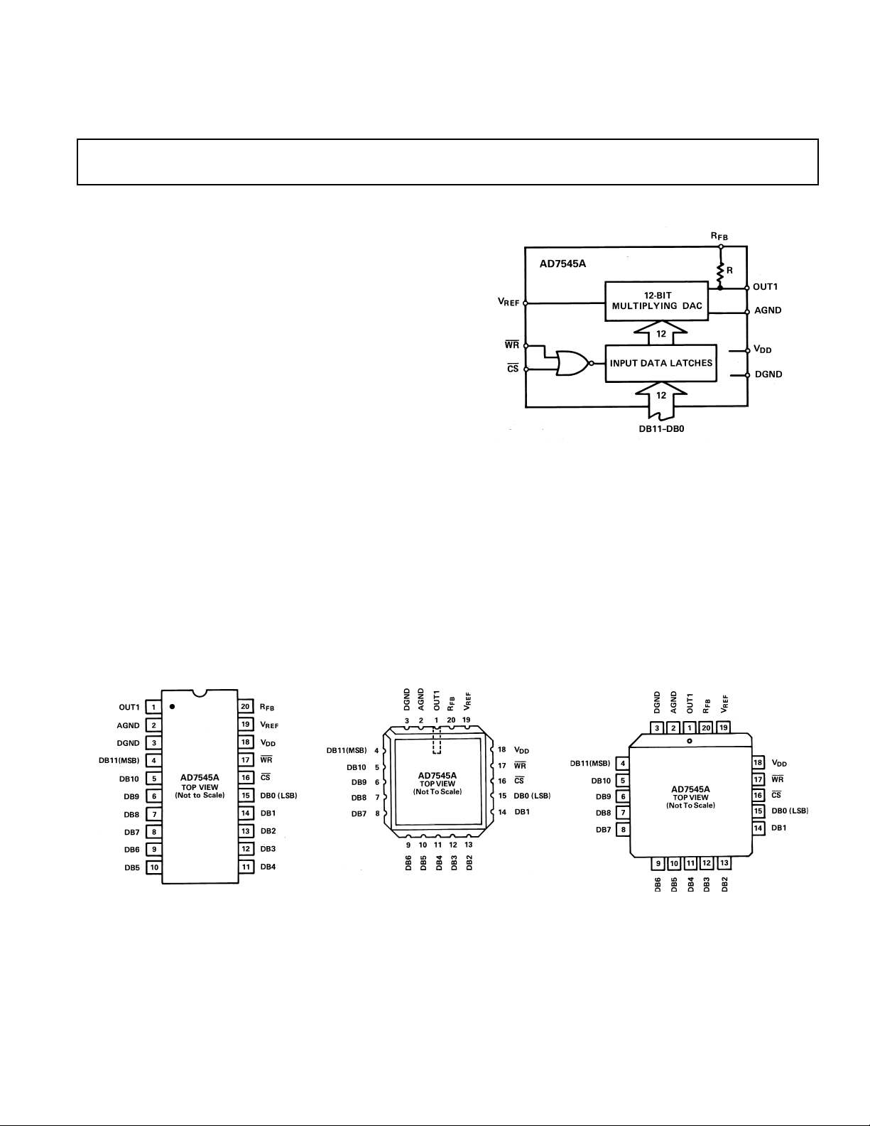
The AD7545A, a 12-bit CMOS multiplying DAC with internal
data latches, is an improved version of the industry standard
AD7545. This new design features a WR pulse width of 100 ns,
which allows interfacing to a much wider range of fast 8-bit and
16-bit microprocessors. It is loaded by a single 12-bit-wide word
under the control of the CS and WR inputs; tying these control
inputs low makes the input latches transparent, allowing unbuffered operation of the DAC.
Buffered Multiplying DAC
AD7545A
FUNCTIONAL BLOCK DIAGRAM
PIN CONFIGURATIONS
DIP/SOIC LCCC PLCC
REV. C
Information furnished by Analog Devices is believed to be accurate and
reliable. However, no responsibility is assumed by Analog Devices for its
use, nor for any infringements of patents or other rights of third parties
which may result from its use. No license is granted by implication or
otherwise under any patent or patent rights of Analog Devices.
One Technology Way, P.O. Box 9106, Norwood, MA 02062-9106, U.S.A.
Tel: 781/329-4700 World Wide Web Site: http://www.analog.com
Fax: 781/326-8703 © Analog Devices, Inc., 2000
Page 2

AD7545A–SPECIFICATIONS
= ⴞ10 V, V
REF
= O V, AGND = DGND unless otherwise noted)
OUT1
(V
VDD = +5 V VDD = +15 V
Parameter Version TA = + 25ⴗCT
Limits Limits
MIN–TMAX
1
TA = + 25ⴗCT
MIN–TMAX
1
Units Test Conditions/Comments
STATIC PERFORMANCE
Resolution All 12 12 12 12 Bits
Relative Accuracy K, B, T ±1/2 ± 1/2 ±1/2 ±1/2 LSB max
L, C, U ±1/2 ±1/2 ±1/2 ± 1/2 LSB max Endpoint Measurement
Differential Nonlinearity All ±1 ±1 ±1 ±1 LSB max All Grades Guaranteed 12-Bit
Monotonic Over Temperature
Gain Error K, B, T ±3 ± 4 ±3 ±4 LSB max Measured Using Internal R
L, C, U ±1 ±2 ±1 ±2 LSB max DAC Register Loaded with All 1s.
Gain Temperature Coefficient
∆Gain/∆Temperature All ±2 ± 2 ± 2 ± 2 ppm/°C typ
DC Supply Rejection
∆Gain/∆V
Output Leakage Current at OUT1 K, L 10 50 10 50 nA max DB0–DB11 = 0 V; WR, CS = 0 V
DD
2
All ±5 ± 5 ± 5 ± 5 ppm/°C max
2
All 0.002 0.004 0.002 0.004 % per % max ∆VDD = ±5%
.
FB
B, C 10 50 10 50 nA max
T, U 10 200 10 200 nA max
DYNAMIC PERFORMANCE
Current Settling Time
Propagation Delay
2
2
(from Digital
All 1 1 1 1 µs max To 1/2 LSB. OUT1 Load = 100 Ω,
= 13 pF. DAC Output Measured
C
EXT
from Falling Edge of WR, CS = 0 V.
Input Change to 90%
of Final Analog Output) All 200 – 150 – ns max OUT1 Load = 100 Ω, C
Digital-to-Analog Glitch Impulse All 5 – 5 – nV sec typ V
AC Feedthrough
2, 4
At OUT1 All 5 5 5 5 mV p-p typ V
= AGND. OUT1 Load = 100 Ω,
REF
Alternately Loaded with All 0s and 1s.
= ±10 V, 10 kHz Sine Wave
REF
EXT
= 13 pF
REFERENCE INPUT
Input Resistance All 10 10 10 10 kΩ min Input Resistance TC = –300 ppm/°C typ
(Pin 19 to GND) 20 20 20 20 kΩ max Typical Input Resistance = 15 kΩ
ANALOG OUTPUTS
Output Capacitance
C
OUT1
C
OUT1
2
All 70 70 70 70 pF max DB0–DB11 = 0 V, WR, CS = 0 V
150 150 150 150 pF max DB0–DB11 = VDD, WR, CS = 0 V
DIGITAL INPUTS
Input High Voltage
V
IH
Input Low Voltage
V
IL
Input Current
I
IN
Input Capacitance
5
2
All 2.4 2.4 13.5 13.5 V min
All 0.8 0.8 1.5 1.5 V max
All ±1 ± 10 ±1 ±10 µA max VIN = 0 or V
DD
DB0–DB11, WR, CS All 8 8 8 8 pF max
SWITCHING CHARACTERISTICS
2
Chip Select to Write Setup Time K, B, L, C 100 130 75 85 ns min See Timing Diagram
t
CS
Chip Select to Write Hold Time
t
CH
Write Pulse Width K, B, L, C 100 130 75 85 ns min t
t
WR
Data Setup Time
t
DS
Data Hold Time
t
DH
T, U 100 170 75 95 ns min
All 0 0 0 0 ns min
T, U 100 170 75 95 ns min
All 100 150 60 80 ns min
All 5 5 5 5 ns min
≥ tWR, TCH ≥ 0
CS
POWER SUPPLY
V
DD
I
DD
NOTES
1
Temperature range as follows: K, L Versions = 0°C to +70°C; B, C Versions = –25°C to +85°C; T, U Versions = –55°C to +125°C.
2
Sample tested to ensure compliance.
3
DB0–DB11 = 0 V to VDD or VDD to 0 V.
4
Feedthrough can be further reduced by connecting the metal lid on the ceramic package to DGND.
6
Logic inputs are MOS gates. Typical input current (+25°C) is less than 1 nA.
All 5 5 15 15 V ±5% For Specified Performance
All 2 2 2 2 mA max All Digital Inputs VIL or V
100 100 100 100 µA max All Digital Inputs 0 V or V
10 10 10 10 µA typ All Digital Inputs 0 V or V
IH
DD
DD
Specifications subject to change without notice.
3
–2–
REV. C
Page 3
WRITE CYCLE TIMING DIAGRAM
WARNING!
ESD SENSITIVE DEVICE
AD7545A
ABSOLUTE MAXIMUM RATINGS*
(TA = + 25°C unless otherwise noted)
VDD to DGND . . . . . . . . . . . . . . . . . . . . . . . . . –0.3 V, +17 V
Digital Input Voltage to DGND . . . . . . . –0.3 V, V
, V
V
V
RFB
PIN1
to DGND . . . . . . . . . . . . . . . . . . . . . . . . . ± 25 V
REF
to DGND . . . . . . . . . . . . . . . . . . . . –0.3 V, VDD +0.3 V
AGND to DGND . . . . . . . . . . . . . . . . . . –0.3 V, V
+0.3 V
DD
+0.3 V
DD
Power Dissipation (Any Package) to 75°C . . . . . . . . . 450 mW
Derates above 75°C by . . . . . . . . . . . . . . . . . . . . . 6 mW/°C
Operating Temperature Range
Commercial (KN, LN, KP, LP) Grades . . . 0°C to +70°C
Industrial (BQ, CQ, BE, CE) Grades . . . . –25°C to +85°C
Extended (TQ, UQ, TE, UE) Grades . . . –55°C to +125°C
Storage Temperature . . . . . . . . . . . . . . . . . . –65°C to +150°C
Lead Temperature (Soldering, 10 secs) . . . . . . . . . . . +300°C
*Stresses above those listed under Absolute Maximum Ratings may cause perma-
nent damage to the device. This is a stress rating only; functional operation of the
device at these or any other conditions above those indicated in the operational
sections of this specification is not implied. Exposure to absolute maximum rating
conditions for extended periods may affect device reliability.
CAUTION
ESD (electrostatic discharge) sensitive device. The digital control inputs are diode protected;
however, permanent damage may occur on unconnected devices subject to high energy electrostatic fields. Unused devices must be stored in conductive foam or shunts. The protective foam
should be discharged to the destination socket before devices are removed.
ORDERING GUIDE
1
Model
AD7545AKN 0°C to +70°C ±1/2 ±4 N-20
AD7545ALN 0°C to +70°C ±1/2 ±2 N-20
AD7545AKR 0°C to +70°C ±1/2 ±4R-20
AD7545AKP 0°C to +70°C ±1/2 ±4 P-20A
AD7545ALP 0°C to +70°C ±1/2 ±2 P-20A
AD7545ABQ –25°C to +85°C ±1/2 ±4 Q-20
AD7545ACQ –25°C to +85°C ± 1/2 ±2 Q-20
AD7545ABE –25°C to +85°C ± 1/2 ±4 E-20A
AD7545ACE –25°C to +85°C ± 1/2 ±2 E-20A
AD7545ATQ –55°C to +125°C ± 1/2 ±4 Q-20
AD7545AUQ –55°C to +125°C ±1/2 ±2 Q-20
AD7545ATE –55°C to +125°C ±1/2 ±4 E-20A
AD7545AUE –55°C to +125°C ±1/2 ±2 E-20A
NOTES
1
To order MIL-STD-883, Class B process parts, add /883B to part number.
Contact local sales office for military data sheet.
2
E = Leadless Ceramic Chip Carrier (LCCC); N = Plastic DIP; P = Plastic
Leaded Chip Carrier (PLCC); Q = Cerdip; R = Small Outline IC.
Temperature Accuracy Error Package
Range T
Relative Gain
MIN–TMAXTMIN–TMAX
Options
2
–3–REV. C
Page 4

AD7545A
CIRCUIT INFORMATION—D/A CONVERTER SECTION
Figure 1 shows a simplified circuit of the D/A converter section
of the AD7545A, and Figure 2 gives an approximate equivalent
circuit. Note that the ladder termination resistor is connected to
AGND. R is typically 15 kΩ.
The binary weighted currents are switched between the OUT1
bus line and AGND by N-channel switches, thus maintaining a
constant current in each ladder leg independent of the switch
state.
Figure 1. Simplified D/A Circuit of AD7545A
The capacitance at the OUT1 bus line, C
OUT1
, is codedependent and varies from 70 pF (all switches to AGND) to
150 pF (all switches to OUT1).
One of the current switches is shown in Figure 2. The input
resistance at V
the V
pin is constant, the reference terminal can be driven by
REF
(Figure 1) is always equal to R. Since RIN at
REF
a reference voltage or a reference current, ac or dc, of positive or
negative polarity. (If a current source is used, a low temperature
coefficient external R
is recommended to define scale factor.)
FB
input buffers operate in their linear region and draw current
from the power supply. To minimize power supply currents it is
recommended that the digital input voltages be as close to the
supply rails (V
and DGND) as is practically possible.
DD
The AD7545A may be operated with any supply voltage in the
range 5 ≤ V
≤ 15 volts. With VDD = +15 V the input logic
DD
levels are CMOS compatible only, i.e., 1.5 V and 13.5 V.
BASIC APPLICATIONS
Figures 4 and 5 show simple unipolar and bipolar circuits using
the AD7545A. Resistor R1 is used to trim for full scale. The L,
C, U grades have a guaranteed maximum gain error of ±1 LSB
at +25°C, and in many applications it should be possible to
dispense with gain trim resistors altogether. Capacitor C1 provides phase compensation and helps prevent overshoot and
ringing when using high speed op amps. Note that all the circuits of Figures 4, 5 and 6 have constant input impedance at the
terminal.
V
REF
The circuit of Figure 4 can either be used as a fixed reference
D/A converter so that it provides an analog output voltage in the
range 0 to –V
or V
can be an ac signal in which case the circuit behaves as
IN
an attenuator (2-Quadrant Multiplier). V
in the range –20 ≤ V
handle such voltages) since V
(note the inversion introduced by the op amp)
IN
can be any voltage
≤ +20 volts (provided the op amp can
IN
is permitted to exceed VDD.
REF
IN
Table II shows the code relationship for the circuit of Figure 4.
Figure 2. N-Channel Current Steering Switch
CIRCUIT INFORMATION—DIGITAL SECTION
Figure 3 shows the digital structure for one bit.
The digital signals CONTROL and CONTROL are generated
from CS and WR.
Figure 3. Digital Input Structure
The input buffers are simple CMOS inverters designed such
that when the AD7545A is operated with V
= 5 V, the buffers
DD
convert TTL input levels (2.4 V and 0.8 V) into CMOS logic
levels. When V
is in the region of 2.0 volts to 3.5 volts, the
IN
Figure 4. Unipolar Binary Operation
Table I. Recommended Trim Resistor Values vs. Grades
Trim Resistor K/B/T L/C/U
R1 200 Ω 100 Ω
R2 68 Ω 33 Ω
Table II. Unipolar Binary Code Table for Circuit of Figure 4
Binary Number in
DAC Register Analog Output
4095
1 1 1 1 1 1 1 1 1 1 1 1 –V
1 0 0 0 0 0 0 0 0 0 0 0 –VIN
0 0 0 0 0 0 0 0 0 0 0 1 –VIN
4096
2048
4096
4096
1
= –1/2 V
IN
0 0 0 0 0 0 0 0 0 0 0 0 0 Volts
–4–
IN
REV. C
Page 5

Figure 5 and Table III illustrate the recommended circuit and
code relationship for bipolar operation. The D/A function itself
uses offset binary code and inverter U
on the MSB line con-
1
verts twos complement input code to offset binary code. If appropriate, inversion of the MSB may be done in software using
an exclusive –OR instruction and the inverter omitted. R3, R4
and R5 must be selected to match within 0.01%, and they
should be the same type of resistor (preferably wire-wound or
metal foil), so that their temperature coefficients match. Mismatch of R3 value to R4 causes both offset and full-scale error.
Mismatch of R5 to R4 and R3 causes full-scale error.
Figure 5. Bipolar Operation (Twos Complement Code)
Table III. Twos Complement Code Table for Circuit of
Figure 5
Data Input Analog Output
2047
0 1 1 1 1 1 1 1 1 1 1 1 +V
0 0 0 0 0 0 0 0 0 0 0 1 +VIN ×
×
2048
1
2048
IN
0 0 0 0 0 0 0 0 0 0 0 0 0 Volts
1
1 1 1 1 1 1 1 1 1 1 1 1 –V
1 0 0 0 0 0 0 0 0 0 0 0 –VIN ×
×
2048
2048
2048
IN
Figure 6 and Table IV show an alternative method of achieving
bipolar output. The circuit operates with sign plus magnitude
code and has the advantage that it gives 12-bit resolution in
each quadrant compared with 11-bit resolution per quadrant for
the circuit of Figure 5. The AD7592 is a fully protected CMOS
change-over switch with data latches. R4 and R5 should match
each other to 0.01% to maintain the accuracy of the D/A converter. Mismatch between R4 and R5 introduces a gain error.
Refer to Reference 1 (supplemental application material) for
additional information on these circuits.
AD7545A
Figure 6. 12-Bit Plus Sign Magnitude Converter
Table IV. 12-Bit Plus Sign Magnitude Code Table for Circuit
of Figure 6
Sign Binary Numbers in
Bit DAC Register Analog Output
4095
0 1 1 1 1 1 1 1 1 1 1 1 1 + V
0 0 0 0 0 0 0 0 0 0 0 0 0 0 Volts
1 0 0 0 0 0 0 0 0 0 0 0 0 0 Volts
1 1 1 1 1 1 1 1 1 1 1 1 1 – VIN ×
Note: Sign bit of “0” connects R3 to GND.
APPLICATIONS HINTS
Output Offset: CMOS D/A converters such as Figures 4, 5
and 6 exhibit a code dependent output resistance which, in turn,
can cause a code dependent error voltage at the output of the
amplifier. The maximum amplitude of this error, which adds
to the D/A converter nonlinearity, depends on V
is the amplifier input offset voltage. To maintain specified accuracy
with V
0.25 mV, or (25 × 10
at 10 V, it is recommended that VOS be no greater than
REF
–6
) (V
), over the temperature range of
REF
operation. Suitable op amps are AD517 and AD711. The AD517
is best suited for fixed reference applications with low bandwidth requirements: it has extremely low offset (150 µV max for
lowest grade) and in most applications will not require an offset
trim. The AD711 has a much wider bandwidth and higher slew
rate and is recommended for multiplying and other applications
requiring fast settling. An offset trim on the AD711 may be
necessary in some circuits.
General Ground Management: AC or transient voltages
between AGND and DGND can cause noise injection into the
analog output. The simplest method of ensuring that voltages at
AGND and DGND are equal is to tie AGND and DGND
together at the AD7545A. In more complex systems where the
AGND and DGND intertie is on the backplane, it is recommended that two diodes be connected in inverse parallel between
the AD7545A AGND and DGND pins (1N914 or equivalent).
×
IN
, where V
OS
4096
4095
4096
OS
–5–REV. C
Page 6

AD7545A
Invalid Data: When WR and CS are both low, the latches are
transparent and the D/A converter inputs follow the data inputs.
In some bus systems, data on the data bus is not always valid for
the whole period during which WR is low, and as a result invalid
data can briefly occur at the D/A converter inputs during a write
cycle. Such invalid data can cause unwanted signals or glitches
at the output of the D/A converter. The solution to this problem, if it occurs, is to retime the write pulse, WR, so it only
occurs when data is valid.
Digital Glitches: Digital glitches result due to capacitive coupling from the digital lines to the OUT1 and AGND terminals.
This should be minimized by screening the analog pins of the
AD7545A (Pins 1, 2, 19, 20) from the digital pins by a ground
track run between Pins 2 and 3 and between Pins 18 and 19 of
the AD7545A.
Note how the analog pins are at one end (DIP) or side (LCC
and PLCC) of the package and separated from the digital pins
by V
and DGND to aid screening at the board level. On-chip
DD
capacitive coupling can also give rise to crosstalk from the digitalto-analog sections of the AD7545A, particularly in circuits with
high currents and fast rise and fall times. This type of crosstalk is
minimized by using VDD = +5 volts. However, great care should
be taken to ensure that the +5 V used to power the AD7545A is
free from digitally induced noise.
Temperature Coefficients: The gain temperature coefficient
of the AD7545A has a maximum value of 5 ppm/°C and a typical value of 2 ppm/°C. This corresponds to worst case gain shifts
of 2 LSBs and 0.8 LSBs respectively over a 100°C temperature
range. When trim resistors R1 and R2 (such as in Figure 4) are
used to adjust full-scale range, the temperature coefficient of R1
and R2 should also be taken into account. The reader is referred
to Analog Devices Application Note “Gain Error and Gain
Temperature Coefficient to CMOS Multiplying DACs,” Publication Number E630c–5–3/86.
SINGLE SUPPLY OPERATION
The ladder termination resistor of the AD7545A (Figure 1) is
connected to AGND. This arrangement is particularly suitable
for single supply operation because OUT1 and AGND may be
biased at any voltage between DGND and V
. OUT1 and
DD
AGND should never go more than 0.3 volts less than DGND or
an internal diode will be turned on and a heavy current may
flow that will damage the device. (The AD7545A is, however,
protected from the SCR latchup phenomenon prevalent in many
CMOS devices.)
Figure 7 shows the AD7545A connected in a voltage switching
mode. OUT1 is connected to the reference voltage and AGND
is connected to DGND. The D/A converter output voltage is
available at the V
equal to R. R
pin and has a constant output impedance
REF
is not used in this circuit and should be tied to
FB
OUT1 to minimize stray capacitance effects.
The loading on the reference voltage source is code-dependent
and the response time of the circuit is often determined by the
behavior of the reference voltage with changing load conditions.
To maintain linearity, the voltages at OUT1 and AGND should
remain within 2.5 volts of each other, for a VDD of 15 volts. If
V
is reduced from 15 V, or the differential voltage between
DD
OUT1 and AGND is increased to more than 2.5 V, the differential nonlinearity of the DAC will increase and the linearity of
the DAC will be degraded. Figures 8 and 9 show typical curves
illustrating this effect for various values of reference voltage and
. If the output voltage is required to be offset from ground
V
DD
by some value, then OUT1 and AGND may be biased up. The
effect on linearity and differential nonlinearity will be the same
as reducing V
Figure 8. Differential Nonlinearity vs. VDD for Figure 7
Circuit. Reference Voltage = 2.5 Volts. Shaded Area Shows
Range of Values of Differential Nonlinearity that Typically
Occur for all Grades.
by the amount of the offset.
DD
Figure 7. Single Supply Operation Using Voltage Switching Mode
Figure 9. Differential Nonlinearity vs. Reference Voltage
for Figure 7 Circuit. V
Range of Values of Differential Nonlinearity that Typically
Occur for all Grades.
= 15 Volts. Shaded Area Shows
DD
–6–
REV. C
Page 7

AD7545A
The circuits of Figures 4, 5 and 6 can all be converted to single
supply operation by biasing AGND to some voltage between
V
and DGND. Figure 10 shows the 2s Complement Bipolar
DD
circuit of Figure 5 modified to give a range from +2 V to +8 V
about a “pseudo-analog ground” of 5 V. This voltage range
would allow operation from a single V
of +10 V to +15 V.
DD
The AD584 pin-programmable reference fixes AGND at +5 V.
is set at +2 V by means of the series resistors R1 and R2.
V
IN
There is no need to buffer the V
input to the AD7545A with
REF
an amplifier because the input impedance of the D/A converter
is constant. Note, however, that since the temperature coefficient
of the D/A reference input resistance is typically –300 ppm/°C,
applications which experience wide temperature variations may
require a buffer amplifier to generate the +2.0 V at the AD7545A
pin. Other output voltage ranges can be obtained by changing
V
REF
R4 to shift the zero point and (R1 + R2) to change the slope, or
gain of the D/A transfer function. V
must be kept at least 5 V
DD
above OUT1 to ensure that linearity is preserved.
Figure 12 shows an alternative approach for use with 8-bit processors which have a full 16-bit wide address bus such as 6800,
8080, Z80. This technique uses the 12 lower address lines of the
processor address bus to supply data to the DAC, thus each
AD7545A connected in this way uses 4k bytes of address locations. Data is written to the DAC using a single memory write
instruction. The address field of the instruction is organized so
that the lower 12 bits contain the data for the DAC and the
upper 4 bits contain the address of the 4k block at which the
DAC resides.
Figure 10. Single Supply "Bipolar" 2s Complement D/A
Converter
MICROPROCESSOR INTERFACING OF THE AD7545A
The AD7545A can interface directly to both 8- and 16-bit
microprocessors via its 12-bit wide data latch using standard CS
and WR control signals.
A typical interface circuit for an 8-bit processor is shown in
Figure 11. This arrangement uses two memory addresses, one
for the lower 8 bits of data to the DAC and one for the upper 4
bits of data into the DAC via the latch.
Figure 12. Connecting the AD7545A to 8-Bit Processors
via the Address Bus
SUPPLEMENTAL APPLICATION MATERIAL
For further information on CMOS multiplying D/A converters
the reader is referred to the following texts:
Reference 1
CMOS DAC Application Guide available from Analog Devices,
Publication Number G872a-15-4/86.
Reference 2
Gain Error and Gain Temperature Coefficient of CMOS
Multiplying DACs – Application Note, Publication Number
E630c–5–3/86.
Reference 3
Analog-Digital Conversion Handbook (Third Edition) available
from Prentice-Hall.
Figure 11. 8-Bit Processor to AD7545 Interface
–7–REV. C
Page 8

AD7545A
OUTLINE DIMENSIONS
Dimensions shown in inches and (mm).
0.5118 (13.00)
0.4961 (12.60)
20 11
PIN 1
0.0118 (0.30)
0.0040 (0.10)
0.0500
(1.27)
BSC
20-Lead SOIC
(R-20)
101
0.1043 (2.65)
0.0926 (2.35)
0.0192 (0.49)
0.0138 (0.35)
SEATING
PLANE
20-Lead Cerdip
(Q-20)
0.2992 (7.60)
0.2914 (7.40)
0.4193 (10.65)
0.3937 (10.00)
0.0125 (0.32)
0.0091 (0.23)
0.0291 (0.74)
0.0098 (0.25)
0.0500 (1.27)
8°
0°
0.0157 (0.40)
20-Lead Plastic DIP
(N-20)
C1022–0–3/00 (rev. C)
x 45°
20-Terminal Leadless Ceramic Chip Carrier
(E-20A)
20-Terminal Plastic Leadless Chip Carrier
(P-20A)
–8–
PRINTED IN U.S.A.
REV. C
 Loading...