

Page 1
CMOS
10kΩ 10kΩ 10kΩ
20kΩ 20kΩ 20kΩ 20kΩ 20kΩ
S1 S2 S3 S12
V
REF
OUT2
OUT1
R
FEEDBACK
BIT 12 (LSB)BIT 3BIT 2BIT 1 (MSB)
DIGITAL INPUTS (DTL/TTL/CMOS COMPATIBLE)
LOGIC: A SWITCH IS CLOSED TO I
OUT1
FOR
ITS DIGITAL INPUT IN A "HIGH" STATE.
10kΩ
a
12-Bit Monolithic Multiplying DAC
AD7541A
FEATURES
Improved Version of AD7541
Full Four-Quadrant Multiplication
12-Bit Linearity (Endpoint)
All Parts Guaranteed Monotonic
TTL/CMOS Compatible
Low Cost
Protection Schottky Diodes Not Required
Low Logic Input Leakage
GENERAL DESCRIPTION
The Analog Devices AD7541A is a low cost, high performance
12-bit monolithic multiplying digital-to-analog converter. It is
fabricated using advanced, low noise, thin film on CMOS
technology and is available in a standard 18-lead DIP and in
20-terminal surface mount packages.
The AD7541A is functionally and pin compatible with the industry standard AD7541 device and offers improved specifications and performance. The improved design ensures that the
device is latch-up free so no output protection Schottky diodes
are required.
This new device uses laser wafer trimming to provide full 12-bit
endpoint linearity with several new high performance grades.
ORDERING GUIDE
2
Model
AD7541AJN 0°C to +70°C ±1 LSB ±6 LSB N-18
AD7541AKN 0°C to +70°C ±1/2 LSB ±1 LSB N-18
AD7541AJP 0°C to +70°C ±1 LSB ±6 P-20A
AD7541AKP 0°C to +70°C ±1/2 LSB ±1 P-20A
AD7541AKR 0°C to +70°C ±1/2 LSB ±1 R-18
AD7541AAQ –25°C to +85°C ±1 LSB ±6 LSB Q-18
AD7541ABQ –25°C to +85°C ±1/2 LSB ±1 LSB Q-18
AD7541ASQ –55°C to +125°C ± 1 LSB ±6 LSB Q-18
AD7541ATQ –55°C to +125°C ±1/2 LSB ±1 LSB Q-18
AD7541ASE –55°C to +125°C ±1 LSB ±6 LSB E-20A
AD7541ATE –55°C to +125°C ±1/2 LSB ±1 LSB E-20A
NOTES
1
Analog Devices reserves the right to ship either ceramic (D-18) or cerdip (Q-18)
hermetic packages.
2
To order MIL-STD-883, Class B process parts, add /883B to part number. Contact
local sales office for military data sheet.
3
E = Leadless Ceramic Chip Carrier; N = Plastic DIP; P = Plastic Leaded Chip
Carrier; Q = Cerdip; R = Small Outline IC.
Temperature Accuracy Error Package
Range T
Relative Gain
to T
MIN
1
= +258C Options
MAXTA
PRODUCT HIGHLIGHTS
Compatibility: The AD7541A can be used as a direct replace-
ment for any AD7541-type device. As with the Analog Devices
AD7541, the digital inputs are TTL/CMOS compatible and
have been designed to have a ± 1 µA maximum input current
requirement so as not to load the driving circuitry.
Improvements: The AD7541A offers the following improved
specifications over the AD7541:
1. Gain Error for all grades has been reduced with premium
grade versions having a maximum gain error of ±3 LSB.
2. Gain Error temperature coefficient has been reduced to
3
2 ppm/°C typical and 5 ppm/°C maximum.
3. Digital-to-analog charge injection energy for this new device
is typically 20% less than the standard AD7541 part.
4. Latch-up proof.
5. Improvements in laser wafer trimming provides 1/2 LSB max
differential nonlinearity for top grade devices over the operating temperature range (vs. 1 LSB on older 7541 types).
6. All grades are guaranteed monotonic to 12 bits over the
operating temperature range.
FUNCTIONAL BLOCK DIAGRAM
REV. B
Information furnished by Analog Devices is believed to be accurate and
reliable. However, no responsibility is assumed by Analog Devices for its
use, nor for any infringements of patents or other rights of third parties
which may result from its use. No license is granted by implication or
otherwise under any patent or patent rights of Analog Devices.
One Technology Way, P.O. Box 9106, Norwood, MA 02062-9106, U.S.A.
Tel: 617/329-4700 World Wide Web Site: http://www.analog.com
Fax: 617/326-8703 © Analog Devices, Inc., 1997
Page 2

AD7541A–SPECIFICATIONS
(VDD = +15 V, V
TA =T
Parameter Version +258CT
= +10 V; OUT 1 = OUT 2 = GND = 0 V unless otherwise noted)
REF
=
A
MIN, TMAX
1
Units Test Conditions/Comments
ACCURACY
Resolution All 12 12 Bits
Relative Accuracy J, A, S ±1 ±1 LSB max ±1 LSB = ±0.024% of Full Scale
K, B, T ±1/2 ±1/2 LSB max ±1/2 LSB = ±0.012% of Full Scale
Differential Nonlinearity J, A, S ±1 ±1 LSB max All Grades Guaranteed Monotonic
to T
K, B, T ±1/2 ±1/2 LSB max to 12 Bits, T
MIN
Gain Error J, A, S ±6 ± 8 LSB max Measured Using Internal R
MAX
.
and Includes
FB
K, B, T ±3 ±5 LSB max Effect of Leakage Current and Gain TC.
Gain Temperature Coefficient
2
Gain Error Can Be Trimmed to Zero.
DGain/DTemperature All 5 5 ppm/°C max Typical Value Is 2 ppm/°C.
Output Leakage Current
OUT1 (Pin 1) J, K ±5 ±10 nA max All Digital Inputs = 0 V.
A, B ±5 ±10 nA max
S, T ±5 ±200 nA max
OUT2 (Pin 2) J, K ±5 ±10 nA max All Digital Inputs = V
DD
.
A, B ±5 ±10 nA max
S, T ±5 ±200 nA max
REFERENCE INPUT
Input Resistance (Pin 17 to GND) All 7–18 7–18 kΩ min/max Typical Input Resistance = 11 kΩ.
Typical Input Resistance Temperature
Coefficient = –300 ppm/°C.
DIGITAL INPUTS
V
(Input HIGH Voltage) All 2.4 2.4 V min
IH
V
(Input LOW Voltage) All 0.8 0.8 V max
IL
I
(Input Current) All ±1 ±1 µA max Logic Inputs Are MOS Gates. IIN typ (25°C) = 1 nA.
IN
CIN (Input Capacitance)
2
All 8 8 pF max VIN = 0 V
POWER SUPPLY REJECTION
DGain/DV
DD
All ±0.01 ±0.02 % per % max DVDD = ±5%
POWER SUPPLY
V
Range All +5 to +16 +5 to +16 V min/V max Accuracy Is Not Guaranteed Over This Range.
DD
I
DD
All 2 2 mA max All Digital Inputs VIL or VIH.
100 500 µA max All Digital Inputs 0 V or VDD.
AC PERFORMANCE CHARACTERISTICS
These Characteristics are included for Design Guidance only and are not subject to test. VDD = +15 V, VIN = +10 V except where noted,
OUT1 = 0UT2 = GND = 0 V, Output Amp is AD544 except where noted.
TA =T
Parameter Version1+258CT
PROPAGATION DELAY (From Digital Input OUT 1 Load = 100 Ω, C
Change to 90% of Final Analog Output) All 100 — ns typ Digital Inputs = 0 V to VDD or VDD to 0 V.
DIGITAL TO ANALOG GLITCH V
IMPULSE V
All 1000 — nV-sec typ Measured using Model 50K as output amplifier.
MULTIPLYING FEEDTHROUGH ERROR
(V
to OUT1) All 1.0 — mV p-p typ V
REF
3
OUTPUT CURRENT SETTLING TIME All 0.6 — µs typ To 0.01% of full-scale range.
OUTPUT CAPACITANCE
C
(Pin 1) All 200 200 pF max Digital Inputs
OUT1
C
(Pin 2) All 70 70 pF max = V
OUT2
C
(Pin 1) All 70 70 pF max Digital Inputs
OUT1
C
(Pin 2) All 200 200 pF max = V
OUT2
NOTES
1
Temperature range as follows: J, K versions, 0°C to +70°C; A, B versions, –25°C to +85°C; S, T versions, –55°C to +125°C.
2
Guaranteed by design but not production tested.
3
To minimize feedthrough in the ceramic package (Suffix D) the user must ground the metal lid.
Specifications subject to change without notice.
=
A
MIN, TMAX
1
Units Test Conditions/Comments
= 0 V. All digital inputs 0 V to VDD or
REF
to 0 V.
DD
= ±10 V, 10 kHz sine wave.
REF
OUT 1 Load = 100 Ω, C
Digital Inputs = 0 V to VDD or VDD to 0 V.
IH
IL
= 13 pF.
EXT
= 13 pF.
EXT
–2– REV. B
Page 3
AD7541A
WARNING!
ESD SENSITIVE DEVICE
ABSOLUTE MAXIMUM RATINGS*
(T
= +25°C unless otherwise noted)
A
to GND . . . . . . . . . . . . . . . . . . . . . . . . . . . . . . . . +17 V
V
DD
to GND . . . . . . . . . . . . . . . . . . . . . . . . . . . . . . . . ±25 V
V
REF
to GND . . . . . . . . . . . . . . . . . . . . . . . . . . . . . . . . . ±25 V
V
RFB
Digital Input Voltage to GND . . . . . . . . –0.3 V, V
OUT 1, OUT 2 to GND . . . . . . . . . . . . –0.3 V, V
+ 0.3 V
DD
+ 0.3 V
DD
Power Dissipation (Any Package)
To +75°C . . . . . . . . . . . . . . . . . . . . . . . . . . . . . . . 450 mW
Derates above +75°C . . . . . . . . . . . . . . . . . . . . . . 6 mW/°C
Operating Temperature Range
Commercial (J, K Versions) . . . . . . . . . . . . . 0°C to +70°C
Industrial (A, B Versions) . . . . . . . . . . . . . –25°C to +85°C
Extended (S, T Versions) . . . . . . . . . . . . . –55°C to +125°C
Storage Temperature . . . . . . . . . . . . . . . . . . –65°C to +150°C
Lead Temperature (Soldering, 10 secs) . . . . . . . . . . . +300°C
*Stresses above those listed under Absolute Maximum Ratings may cause perma-
nent damage to the device. This is a stress rating only; functional operation of the
device at these or any other conditions above those indicated in the operational
sections of this specification is not implied. Exposure to absolute maximum rating
conditions for extended periods may affect device reliability.
CAUTION
ESD (electrostatic discharge) sensitive device. Electrostatic charges as high as 4000 V readily
accumulate on the human body and test equipment and can discharge without detection.
Although the AD7541A features proprietary ESD protection circuitry, permanent damage may
occur on devices subjected to high energy electrostatic discharges. Therefore, proper ESD
precautions are recommended to avoid performance degradation or loss of functionality.
TERMINOLOGY
RELATIVE ACCURACY
Relative accuracy or endpoint nonlinearity is a measure of the
OUTPUT LEAKAGE CURRENT
Current which appears at OUTI with the DAC loaded to all 0s
or at OUT2 with the DAC loaded to all 1s.
maximum deviation from a straight line passing through the
endpoints of the DAC transfer function. It is measured after
adjusting for zero and full scale and is expressed in % of fullscale range or (sub)multiples of 1 LSB.
MULTIPLYING FEEDTHROUGH ERROR
AC error due to capacitive feedthrough from V
OUT1 with DAC loaded to all 0s.
terminal to
REF
DIFFERENTIAL NONLINEARITY
Differential nonlinearity is the difference between the measured
change and the ideal l LSB change between any two adjacent
codes. A specified differential nonlinearity of ±1 LSB max over
OUTPUT CURRENT SETTLING TIME
Time required for the output function of the DAC to settle to
within 1/2 LSB for a given digital input stimulus, i.e., 0 to full
scale.
the operating temperature range insures monotonicity.
PROPAGATION DELAY
GAIN ERROR
Gain error is a measure of the output error between an ideal
DAC and the actual device output. For the AD7541A, ideal
This is a measure of the internal delay of the circuit and is measured from the time a digital input changes to the point at which
the analog output at OUT1 reaches 90% of its final value.
maximum output is
4095
(V
–
4096
REF
).
Gain error is adjustable to zero using external trims as shown in
Figures 4, 5 and 6.
DIGITAL-TO-ANALOG CHARGE INJECTION (QDA)
This is a measure of the amount of charge injected from the
digital inputs to the analog outputs when the inputs change
state. It is usually specified as the area of the glitch in nV secs
and is measured with V
= GND and a Model 50K as the
REF
output op amp, C1 (phase compensation) = 0 pF.
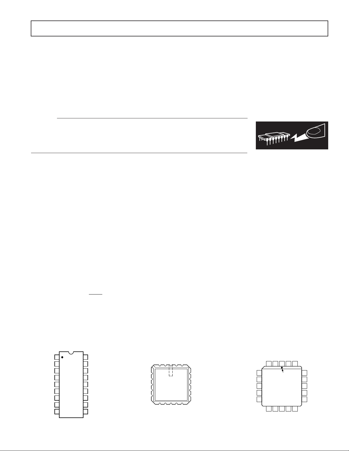
PIN CONFIGURATIONS
DIP/SOIC LCCC PLCC
FB
OUT1
OUT2
GND
BIT 1 (MSB)
BIT 2
BIT 3
BIT 4
BIT 5
BIT 6
1
2
3
4
AD7541A
5
TOP VIEW
(Not to Scale)
6
7
8
9
18
R
FEEDBACK
V
17
REF
16
VDD (+)
15
BIT 12 (LSB)
BIT 11
14
BIT 10
13
12
BIT 9
11
BIT 8
BIT 7
10
OUT 1
IN
4
GND
BIT 2
BIT 3
BIT 4
5
6
7
8
BIT 1 (MSB)
NC = NO CONNECT
20 19123
AD7541A
TOP VIEW
(Not to Scale)
910111213
NC
BIT 7
BIT 5
BIT 6
BIT 8
18
V
DD
17
BIT 12 (LSB)
16
BIT 11
15
BIT 10
14
BIT 9
GND
BIT 1 (MSB)
BIT 2
BIT 3
BIT 4
NC = NO CONNECT
OUT 2
4
5
6
7
8
9101112
BIT 5
AD7541A
(Not to Scale)
REF
R
OUT 2
NC
V
NC
OUT 1
20 19
123
PIN 1
IDENTIFIER
TOP VIEW
BIT 6NCBIT 7
FB
REF
R
V
13
BIT 8
18
V
BIT 12 (LSB)
17
BIT 11
16
15
BIT 10
BIT 9
14
DD
–3–REV. B
Page 4

AD7541A
1816
1
2
3
17
AD7541A
V
DD
R
FB
V
DD
V
REF
PINS 4–15
DGND
OUT1
OUT2
R1
*
V
IN
BIT 1 – BIT 12
DIGITAL
GROUND
ANALOG
COMMON
R2
*
C1
33pF
AD544L
(SEE TEXT)
V
OUT
*REFER TO TABLE 1
GENERAL CIRCUIT INFORMATION
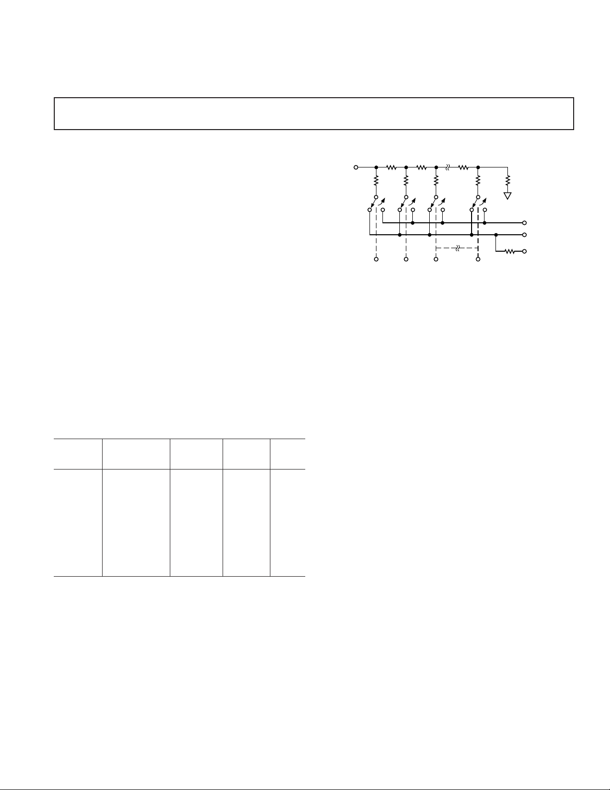
The simplified D/A circuit is shown in Figure 1. An inverted
R-2R ladder structure is used—that is, the binarily weighted
currents are switched between the OUT1 and OUT2 bus lines,
thus maintaining a constant current in each ladder leg independent of the switch state.
V
REF
10kΩ 10kΩ 10kΩ
20kΩ 20kΩ 20kΩ 20kΩ 20kΩ
S1 S2 S3 S12
APPLICATIONS
UNIPOLAR BINARY OPERATION
(2-QUADRANT MULTIPLICATION)
Figure 4 shows the analog circuit connections required for unipolar binary (2-quadrant multiplication) operation. With a dc
reference voltage or current (positive or negative polarity) applied at Pin 17, the circuit is a unipolar D/A converter. With an
ac reference voltage or current, the circuit provides 2-quadrant
multiplication (digitally controlled attenuation). The input/
output relationship is shown in Table II.
R1 provides full-scale trim capability [i.e., load the DAC register
OUT2
OUT1
10kΩ
R
FEEDBACK
BIT 12 (LSB)BIT 3BIT 2BIT 1 (MSB)
DIGITAL INPUTS (DTL/TTL/CMOS COMPATIBLE)
LOGIC: A SWITCH IS CLOSED TO I
ITS DIGITAL INPUT IN A "HIGH" STATE.
OUT1
FOR
Figure 1. Functional Diagram (Inputs HIGH)
The input resistance at V
(R
is the R/2R ladder characteristic resistance and is equal to
LDR
value “R”). Since R
IN
(Figure 1) is always equal to R
REF
at the V
pin is constant, the reference
REF
LDR
terminal can be driven by a reference voltage or a reference
current, ac or dc, of positive or negative polarity. (If a current
source is used, a low temperature coefficient external R
FB
is
to 1111 1111 1111, adjust R1 for V
OUT
= –V
Alternatively, Full Scale can be adjusted by omitting R1 and R2
and trimming the reference voltage magnitude.
C1 phase compensation (10 pF to 25 pF) may be required for
stability when using high speed amplifiers. (C1 is used to cancel
the pole formed by the DAC internal feedback resistance and
output capacitance at OUT1).
Amplifier A1 should be selected or trimmed to provide V
10% of the voltage resolution at V
. Additionally, the ampli-
OUT
fier should exhibit a bias current which is low over the temperature range of interest (bias current causes output offset at V
equal to I
times the DAC feedback resistance, nominally 11 kΩ).
B
The AD544L is a high speed implanted FET input op amp with
low factory-trimmed V
OS
.
(4095/4096)].
REF
OS
≤
OUT
recommended to define scale factor.)
EQUIVALENT CIRCUIT ANALYSIS
The equivalent circuits for all digital inputs LOW and all digital
inputs HIGH are shown in Figures 2 and 3. In Figure 2 with all
digital inputs LOW, the reference current is switched to OUT2.
The current source I
tion leakages to the substrate, while the I/
is composed of surface and junc-
LEAKAGE
current source
4096
represents a constant 1-bit current drain through the termination resistor on the R-2R ladder. The ON capacitance of the
output N-channel switch is 200 pF, as shown on the OUT2
terminal. The OFF switch capacitance is 70 pF, as shown on
the OUT1 terminal. Analysis of the circuit for all digital inputs
HIGH, as shown in Figure 3 is similar to Figure 2; however, the
ON switches are now on terminal OUT1, hence the 200 pF at
that terminal.
R 15kΩ
V
REF
R
I
LEAKAGE
I
REF
I
/4096
I
LEAKAGE
70pF
200pF
RFB
OUT1
OUT2
Table I. Recommended Trim Resistor Values vs. Grades
Table II. Unipolar Binary Code Table for Circuit of Figure 4
Binary Number in DAC
MSB LSB Analog Output, V
Figure 4. Unipolar Binary Operation
Trim
Resistor JN/AQ/SD KN/BQ/TD
R1 100 Ω 100 Ω
R2 47 Ω 33 Ω
OUT
Figure 2. DAC Equivalent Circuit All Digital Inputs LOW
1 1 1 1 1 1 1 1 1 1 1 1 –VIN
1 0 0 0 0 0 0 0 0 0 0 0 –VIN
0 0 0 0 0 0 0 0 0 0 0 1 –VIN
0 0 0 0 0 0 0 0 0 0 0 0 0 Volts
–4– REV. B
RFB
OUT1
OUT2
R 15kΩ
V
REF
I
REF
Figure 3. DAC Equivalent Circuit All Digital Inputs HIGH
I
/4096
I
LEAKAGE
I
LEAKAGE
R
200pF
70pF
4095
4096
2048
4096
1
4096
= –1/2 V
IN
Page 5

AD7541A
A2
AD7541A
A1
3
R2*
V
DD
161718
1
2
VDDR
FB
V
REF
PINS 4–15
GND
OUT1
OUT2
R1*
V
IN
BIT 1 – BIT 12
DIGITAL
GROUND
ANALOG
COMMON
C1
33pF
AD544L
V
OUT
AD544J
R5
20kΩ
*FOR VALUES OF R1 AND R2
SEE TABLE 1.
R4
20kΩ
R3
10kΩ
10%
1/2 AD7592JN
SIGN BIT
BIPOLAR OPERATION
(4-QUADRANT MULTIPLICATION)
Figure 5 and Table III illustrate the circuitry and code relationship for bipolar operation. With a dc reference (positive or negative polarity) the circuit provides offset binary operation. With
an ac reference the circuit provides full 4-quadrant multiplication.
With the DAC loaded to 1000 0000 0000, adjust R1 for
= 0 V (alternatively, one can omit R1 and R2 and adjust
V
OUT
the ratio of R3 to R4 for V
be accomplished by adjusting the amplitude of V
= 0 V). Full-scale trimming can
OUT
or by vary-
REF
ing the value of R5.
As in unipolar operation, A1 must be chosen for low V
. R3, R4 and R5 must be selected for matching and track-
low I
B
OS
and
ing. Mismatch of 2R3 to R4 causes both offset and full-scale
error. Mismatch of R5 to R4 or 2R3 causes full-scale error. C1
phase compensation (10 pF to 50 pF) may be required for stability, depending on amplifier used.
V
DD
161718
VDDR
V
REF
V
R1*
IN
AD7541A
PINS 4–15
BIT 1 – BIT 12
FB
GROUND
OUT1
OUT2
GND
3
DIGITAL
R2*
1
2
ANALOG
COMMON
C1
33pF
A1
AD544L
*FOR VALUES OF R1 AND R2
SEE TABLE 1.
R3
10kΩ
R6
5kΩ
10%
R4
20kΩ
A2
AD544J
R5
20kΩ
V
OUT
Figure 5. Bipolar Operation (4-Quadrant Multiplication)
Table III. Bipolar Code Table for Offset Binary Circuit of
Figure 5
Binary Number in DAC
MSB LSB Analog Output, V
1 1 1 1 1 1 1 1 1 1 1 1 +VIN
1 0 0 0 0 0 0 0 0 0 0 1 +VIN
2047
2048
1
2048
OUT
1 0 0 0 0 0 0 0 0 0 0 0 0 Volts
0 1 1 1 1 1 1 1 1 1 1 1 –V
IN
0 0 0 0 0 0 0 0 0 0 0 0 –VIN
1
2048
2048
2048
Figure 6 and Table IV show an alternative method of achieving
bipolar output. The circuit operates with sign plus magnitude
code and has the advantage of giving 12-bit resolution in each
quadrant, compared with 11-bit resolution per quadrant for the
circuit of Figure 5. The AD7592 is a fully protected CMOS
changeover switch with data latches. R4 and R5 should match
each other to 0.01% to maintain the accuracy of the D/A converter. Mismatch between R4 and R5 introduces a gain error.
Figure 6. 12-Bit Plus Sign Magnitude Operation
Table IV. 12-Bit Plus Sign Magnitude Code Table for Circuit
of Figure 6
Sign Binary Number in DAC
Bit MSB LSB Analog Output, V
0 1 1 1 1 1 1 1 1 1 1 1 1 +V
4095
×
IN
4096
OUT
0 0 0 0 0 0 0 0 0 0 0 0 0 0 Volts
1 0 0 0 0 0 0 0 0 0 0 0 0 0 Volts
1 1 1 1 1 1 1 1 1 1 1 1 1 –V
Note: Sign bit of “0” connects R3 to GND.
4095
×
4096
IN
–5–REV. B
Page 6

AD7541A
APPLICATIONS HINTS
Output Offset: CMOS D/A converters exhibit a code-dependent
output resistance which in turn can cause a code-dependent
error voltage at the output of the amplifier. The maximum amplitude of this offset, which adds to the D/A converter nonlinearity, is 0.67 V
voltage. To maintain monotonic operation it is recommended
that V
be no greater than (25 × 10
OS
where VOS is the amplifier input offset
OS
–6
) (V
) over the tempera-
REF
ture range of operation. Suitable op amps are AD517L and
AD544L. The AD517L is best suited for fixed reference applications with low bandwidth requirements: it has extremely low
offset (50 µV) and in most applications will not require an offset
trim. The AD544L has a much wider bandwidth and higher
slew rate and is recommended for multiplying and other applications requiring fast settling. An offset trim on the AD544L
may be necessary in some circuits.
Digital Glitches: One cause of digital glitches is capacitive
coupling from the digital lines to the OUT1 and OUT2 terminals. This should be minimized by screening the analog pins of
the AD7541A (Pins 1, 2, 17, 18) from the digital pins by a
ground track run between Pins 2 and 3 and between Pins 16
and 17 of the AD7541A. Note how the analog pins are at one
end of the package and separated from the digital pins by V
DD
and GND to aid screening at the board level. On-chip capacitive
coupling can also give rise to crosstalk from the digital-to-analog
sections of the AD7541A, particularly in circuits with high currents and fast rise and fall times.
Temperature Coefficients: The gain temperature coefficient
of the AD7541A has a maximum value of 5 ppm/°C and a typi-
cal value of 2 ppm/°C. This corresponds to worst case gain shifts
of 2 LSBs and 0.8 LSBs, respectively, over a 100°C temperature
range. When trim resistors R1 and R2 are used to adjust fullscale range, the temperature coefficient of R1 and R2 should
also be taken into account. The reader is referred to Analog
Devices Application Note “Gain Error and Gain Temperature
Coefficient of CMOS Multiplying DACs,” Publication Number
E630c-5-3/86.
SINGLE SUPPLY OPERATION
Figure 7 shows the AD7541A connected in a voltage switching
mode. OUT1 is connected to the reference voltage and OUT2
is connected to GND. The D/A converter output voltage is
available at the V
impedance equal to R
pin (Pin 17) and has a constant output
REF
. The feedback resistor RFB is not used
LDR
in this circuit.
NOT
USED
R
1
V
REF
+2.5V
OUT1
2
OUT2
GND
3
±V
V
OUT
i.e., D IS A FRACTIONAL REPRESENTATION OF THE DIGITAL INPUT
D (1 +R2/R1) WHERE 0 ≤ D ≤ 1
REF
FB
AD7541A
PINS 4–15
BIT 1 – BIT 12
1618
V
DD
V
REF
CA3140B
17
154
R2
R1
30kΩ
10kΩ
V+
V–
VDD = +15V
V
= 0V TO +10V
OUT
SYSTEM
GROUND
Figure 7. Single Supply Operation Using Voltage Switching Mode
The reference voltage must always be positive. If OUT1 goes
more than 0.3 V less than GND, an internal diode will be turned
on and a heavy current may flow causing device damage (the
AD7541A is, however, protected from the SCR latch-up
phenomenon prevalent in many CMOS devices). Suitable references include the AD580 and AD584.
The loading on the reference voltage source is code-dependent
and the response time of the circuit is often determined by the
behavior of the reference voltage with changing load conditions.
To maintain linearity, the voltage at OUT1 should remain within
2.5 V of GND, for a V
of 15 V. If VDD is reduced from 15 V
DD
or the reference voltage at OUT1 increased to more than 2.5 V,
the differential nonlinearity of the DAC will increase and the
linearity of the DAC will be degraded.
SUPPLEMENTAL APPLICATION MATERIAL
For further information on CMOS multiplying D/A converters,
the reader is referred to the following texts:
CMOS DAC Application Guide, Publication Number
G872b-8-1/89 available from Analog Devices.
Gain Error and Gain Temperature Coefficient of CMOS
Multiplying DACs Application Note, Publication Number
E630c-5-3/86 available from Analog Devices.
Analog-Digital Conversion Handbook—available from Analog
Devices.
–6– REV. B
Page 7

0.200 (5.08)
)
OUTLINE DIMENSIONS
3
PIN 1
IDENTIFIER
4
19
18
8
9
14
13
TOP VIEW
(PINS DOWN)
0.395 (10.02)
0.385 (9.78)
SQ
0.356 (9.04)
0.350 (8.89)
SQ
0.048 (1.21)
0.042 (1.07)
0.048 (1.21)
0.042 (1.07)
0.020
(0.50)
R
0.050
(1.27)
BSC
0.021 (0.53)
0.013 (0.33)
0.330 (8.38)
0.290 (7.37)
0.032 (0.81)
0.026 (0.66)
0.180 (4.57)
0.165 (4.19)
0.040 (1.01)
0.025 (0.64)
0.056 (1.42)
0.042 (1.07)
0.025 (0.63)
0.015 (0.38)
0.110 (2.79)
0.085 (2.16)
18
1
9
10
0.310 (7.87)
0.220 (5.59)
PIN 1
0.005 (0.13) MIN
0.098 (2.49) MAX
SEATING
PLANE
0.023 (0.58)
0.014 (0.36)
0.200 (5.08)
MAX
0.960 (24.38) MAX
0.150
(3.81)
MIN
0.070 (1.78)
0.030 (0.76)
0.200 (5.08)
0.125 (3.18)
0.100
(2.54)
BSC
0.060 (1.52)
0.015 (0.38)
15°
0°
0.320 (8.13)
0.290 (7.37)
0.015 (0.38)
0.008 (0.20)
SEATING
PLANE
0.0118 (0.30)
0.0040 (0.10)
0.0192 (0.49)
0.0138 (0.35)
0.1043 (2.65)
0.0926 (2.35)
0.0500
(1.27)
BSC
0.0125 (0.32)
0.0091 (0.23)
0.0500 (1.27)
0.0157 (0.40)
8°
0°
0.0291 (0.74)
0.0098 (0.25)
x 45°
18 10
91
0.4625 (11.75)
0.4469 (11.35)
0.4193 (10.65)
0.3937 (10.00)
0.2992 (7.60)
0.2914 (7.40)
PIN 1
Dimensions shown in inches and (mm).
AD7541A
20-Terminal Ceramic Leadless Chip Carrier
(E-20A)
BSC
REF
0.055 (1.40)
0.045 (1.14)
0.075
(1.91)
REF
19
18
14
13
20
1
BOTTOM
VIEW
0.150 (3.81)
0.358 (9.09)
0.342 (8.69)
SQ
0.100 (2.54)
0.064 (1.63)
0.358
(9.09)
MAX
SQ
0.088 (2.24)
0.054 (1.37)
0.095 (2.41)
0.075 (1.90)
0.011 (0.28)
0.007 (0.18)
R TYP
0.075 (1.91)
18-Lead Plastic DIP
(N-18)
0.925 (23.49
0.845 (21.47)
0.210
(5.33)
MAX
0.160 (4.06)
0.115 (2.93)
18
19
PIN 1
0.022 (0.558)
0.014 (0.356)
0.100
(2.54)
BSC
10
0.070 (1.77)
0.045 (1.15)
0.280 (7.11)
0.240 (6.10)
0.060 (1.52)
0.015 (0.38)
0.130
(3.30)
MIN
SEATING
PLANE
0.100 (2.54) BSC
3
4
8
9
45° TYP
BSC
0.325 (8.25)
0.300 (7.62)
0.015 (0.38)
MIN
0.028 (0.71)
0.022 (0.56)
0.050 (1.27)
BSC
0.195 (4.95)
0.115 (2.93)
0.015 (0.381)
0.008 (0.204)
20-Lead Plastic Leadless Chip Carrier
(P-20A)
18-Lead Cerdip
(Q-18)
18-Lead SOIC
(R-18)
–7–REV. B
Page 8

C718b–1–6/97
–8–
PRINTED IN U.S.A.
 Loading...