

Page 1
LC2MOS
V
V
Microprocessor-Compatible 14-Bit DAC
FEATURES
All grades 14-bit monotonic over the full temperature range
Low cost, 14-bit upgrade for 12-bit systems
14-bit parallel load with double buffered inputs
Small 24-pin, 0.30” DIP and SOIC
Low output leakage (<20 nA) over the full temperature range
APPLICATIONS
Microprocessor-based control systems
Digital audio
Precision servo control
Control and measurement in high temperature environments
GENERAL DESCRIPTION
The AD7538 is a 14-bit monolithic CMOS digital-to-analog
converter (DAC) that uses laser trimmed thin-film resistors to
achieve excellent linearity.
The DAC is loaded by a single 14-bit wide word using standard
chip select and memory write logic. Double buffering, which is
optional using
containing multiple AD7538s.
A novel low leakage configuration enables the AD7538 to
exhibit excellent output leakage current characteristics over
the specified temperature range.
The AD7538 is manufactured using the linear-compatible
CMOS (LC
microprocessors and accepts TTL or CMOS logic level inputs.
LDAC
, allows simultaneous updates in a system
2
MOS) process. It is speed compatible with most
AD7538
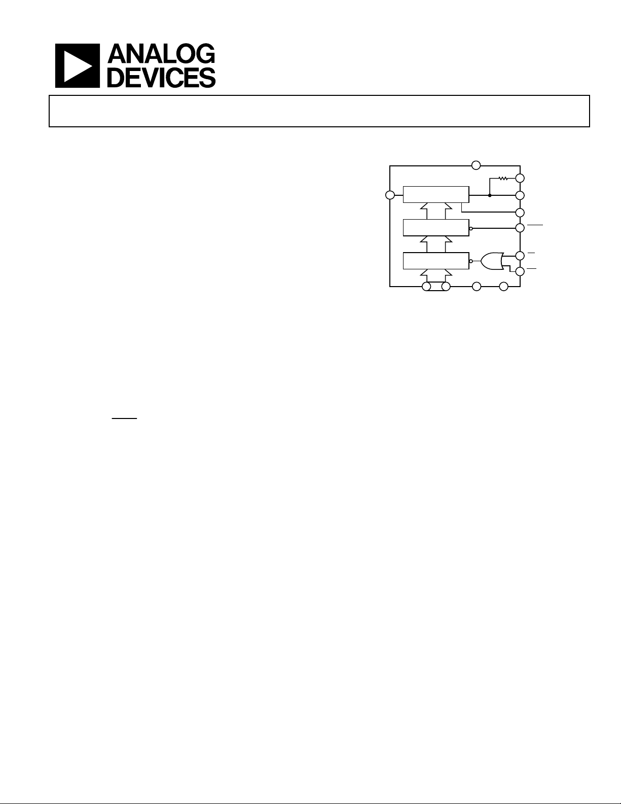
FUNCTIONAL BLOCK DIAGRAM
DD
23
AD7538
14-BIT DAC
1
REF
DAC REGISTER
INPUT
REGISTER
14
619
DB13 TO DB0 DGND
Figure 1.
PRODUCT HIGHLIGHTS
1. Guaranteed Monotonicity.
The AD7538 is guaranteed monotonic to 14-bits over the
full temperature range for all grades.
2. Low Cost.
The AD7538, with its 14-bit dynamic range, affords a low
cost solution for 12-bit system upgrades.
3. Small Package Size.
The AD7538 is packaged in a small 24-pin, 0.3" DIP and a
24-pin SOIC.
4. Low Output Leakage.
By tying V
achieve a low output leakage current at high temperatures.
5. Wide Power Supply Tolerance.
The device operates on a +12 V to +15 V V
tolerance on this nominal figure. All specifications are
guaranteed over this range.
(Pin 24) to a negative voltage, it is possible to
SS
2
R
FB
3
I
OUT
4
AGND
20
LDAC
21
CS
22
WR
245
V
SS
, with a ±5%
DD
01139-001
Rev. B
Information furnished by Analog Devices is believed to be accurate and reliable. However, no
responsibility is assumed by Analog Devices for its use, nor for any infringements of patents or other
rights of third parties that may result from its use. Specifications subject to change without notice. No
license is granted by implication or otherwise under any patent or patent rights of Analog Devices.
Trademarks and registered trademarks are the property of their respective owners.
One Technology Way, P.O. Box 9106, Norwood, MA 02062-9106, U.S.A.
Tel: 781.329.4700 www.analog.com
Fax: 781.461.3113 ©2009 Analog Devices, Inc. All rights reserved.
Page 2

AD7538
TABLE OF CONTENTS
Features .............................................................................................. 1
Applications ....................................................................................... 1
Functional Block Diagram .............................................................. 1
General Description ......................................................................... 1
Product Highlights ........................................................................... 1
Revision History ............................................................................... 2
Specifications ..................................................................................... 3
AC Performance Characteristics ................................................ 4
Timing Characteristics ................................................................ 4
Timing Diagram ........................................................................... 5
Absolute Maximum Ratings ............................................................ 6
ESD Caution .................................................................................. 6
Pin Configuration and Function Descriptions ............................. 7
Terminology ...................................................................................... 8
DAC Section ...................................................................................... 9
Circuit Information ........................................................................ 10
Equivalent Circuit Analysis ...................................................... 10
Digital Section ............................................................................ 10
Unipolar Binary Operation (2-Quadrant Multiplication) .... 10
Bipolar Operation (4-Quadrant Multiplication) .................... 11
Low Leakage Configuration ...................................................... 11
Programmable Gain Amplifier ................................................. 12
Application Hints ........................................................................... 13
Output Offset .............................................................................. 13
General Ground Management .................................................. 13
Microprocessor Interfacing ....................................................... 13
AD7538-to-8086 Interface ........................................................ 13
AD7538-to-MC68000 Interface ............................................... 13
Digital Feedthrough ................................................................... 14
Outline Dimensions ....................................................................... 15
Ordering Guide .......................................................................... 16
REVISION HISTORY
1/09—Rev. A to Rev. B
Updated Format .................................................................. Universal
Changes to Table 1 ............................................................................ 3
Updated Outline Dimensions ....................................................... 15
Changes to Ordering Guide .......................................................... 15
5/87—Rev. 0 to Rev. A
Rev. B | Page 2 of 16
Page 3

AD7538
SPECIFICATIONS
VDD = 11.4 V to 15.75 V1, V
Table 1.
Parameter2
ACCURACY
Resolution 14 14 14 14 Bits
Relative Accuracy ±2 ±1 ±2 ±1 LSB max
Differential Nonlinearity ±1 ±1 ±1 ±1 LSB max Over temperature
Full-Scale Error Measured using internal RFB DAC
+25°C ±4 ±4 ±4 ±4 LSB max Registers loaded with all 1s
T
to T
MIN
±8 ±5 ±10 ±6 LSB max
MAX
Gain Temperature Coefficient3;
ΔGain/ΔTemperature
Output Leakage Current
(Pin 3)
I
OUT
25°C ±5 ±5 ±5 ±5 nA max All digital inputs 0 V
T
to T
MIN
T
MIN
±10 ±10 ±20 ±20 nA max VSS = –300 mV
MAX
to T
±25 ±25 ±150 ±150 nA max VSS = 0 V
MAX
REFERENCE INPUT
Input Resistance (Pin 1) 3.5 3.5 3.5 3.5 kΩ min Typical input resistance = 6 kΩ
10 10 10 10 kΩ max
DIGITAL INPUTS
VIH (Input High Voltage) 2.4 2.4 2.4 2.4 V min
VIL (Input Low Voltage) 0.8 0.8 0.8 0.8 V max
IIN (Input Current)
25°C ±1 ±1 ±1 ±1 μA max VIN = 0 V or VDD
T
to T
MIN
±10 ±10 ±10 ±10 μA max
MAX
CIN (Input Capacitance)3 7 7 7 7 pF max
POWER SUPPLY
VDD Range 11.4/15.75 11.4/15.75 11.4/15.75 11.4/15.75 V min/V max
VSS Range −200/−500 −200/−500 −200/−500 −200/−500
IDD 4 4 4 4 mA max All digital inputs are VIL or V
500 500 500 500 μA max All digital inputs are 0 V or V
1
Specifications are guaranteed for a VDD of 11.4 V to 15.75 V. At VDD = 5 V, the device is fully functional with degraded specifications.
2
Temperature range as follows: J, K Versions: 0°C to +70°C
3
Sample tested to ensure compliance.
= 10 V; V
REF
A, J
Versions
PIN3
= V
PIN4
B, K
Versions S Version T Version Unit Test Conditions/Comments
±2 ±2 ±2 ±2 ppm/°C typ
A, B Versions: −25°C to +85°C
S, T Versions: −55°C to +125°C
= 0 V, VSS = −300 mV; all specifications T
to T
MIN
mV min/
mV max
, unless otherwise noted.
MAX
All grades guaranteed
monotonic
Specification guaranteed over
this range
Specification guaranteed over
this range
IH
DD
Rev. B | Page 3 of 16
Page 4
AD7538
AC PERFORMANCE CHARACTERISTICS
These characteristics are included for design guidance only and are not subject to test. VDD = 11.4 V to 15.75 V, V
0 V, V
= 0 V or −300 mV, output amplifier is AD711 except where noted.
SS
Table 2.
T
= 25°C
A
Parameter
TA = T
MIN
, T
MAX
Unit Test Conditions/Comments
Output Current Settling Time 1.5 μs max To 0.003% of full-scale range
load= 100 Ω, C
I
OUT
= 13 pF DAC register alternately loaded
EXT
with all 1s and all 0s; typical value of settling time is 0.8 μs
Digital-to-Analog Glitch Impulse 20 nV-sec typ
Measured with V
REF
= 0 V. I
load = 100 Ω, C
OUT
register alternately loaded with all 1s and all 0s
Multiplying Feedthrough Error 3 5 mV p-p typ V
= ±10 V, 10 kHz sine wave DAC
REF
Register loaded with all 0s
Power Supply Rejection
ΔGain/ΔVDD ±0.01 ±0.02 % per % max ΔVDD = ±5%
Output Capacitance
C
(Pin 3) 260 260 pF max DAC register loaded with all 1s
OUT
C
(Pin 3) 130 130 pF max DAC register loaded with all 0s
OUT
Output Noise Voltage Density
(10 Hz to 100 kHz) 15 nV√Hz typ Measured between RFB and I
OUT
= 10 V, V
REF
= V
PIN3
= 13 pF; DAC
EXT
PIN4
=
TIMING CHARACTERISTICS
VDD = 11.4 V to 15.75 V, V
Figure 2 for a timing diagram.
Table 3.
Limit at
T
Parameter1
t1
t2
t3
= +25°C
A
0 0 0 ns min
0 0 0 ns min
170 200 240 ns min
t4 170 200 240 ns min Write pulse width
t5 140 160 180 ns min Data setup time
t6
1
Temperature range as follows: J, K Versions: 0°C to +70°C
20 20 30 ns min Data hold time
= 10 V, V
REF
PIN3
= V
PIN4
Limit at TA = 0°C to +70°C
TA = −25°C to +85°C
A, B Versions: −25°C to +85°C
S, T Versions: −55°C to +125°C
= 0 V, VSS = 0 V or −300 mV. All specifications T
Limit at
TA = −55°C to +125°C
Unit Test Conditions/Comments
MIN
to T
unless otherwise noted. See
MAX
to WR setup time
CS
CS to WR hold time
LDAC
pulse width
Rev. B | Page 4 of 16
Page 5
AD7538
TIMING DIAGRAM
t
1
CS
LDAC
WR
DATA
NOTES
1. ALL INP UT SIGNAL RISE AND FALL TIMES MEASURES FROM 10%
TO 90% OF 5V,
2. TIMING MEASUREMENT REFERENCE LEVEL IS .
3. IF LDAC I S ACTIVATED PRIOR TO THE RISI NG EDGE O F WR,
THEN IT MUST STAY LOW FOR
t
2
t
4
t
t
t
6
5
=
t
= 20ns.
R
F
t
3
Figure 2. Timing Diagram
t
3
+ V
V
IH
IL
2
OR LONGE R AFTER WR GOES HIGH.
5V
0V
5V
0V
5V
0V
5V
0V
01139-002
Rev. B | Page 5 of 16
Page 6

AD7538
ABSOLUTE MAXIMUM RATINGS
T
= +25°C unless, otherwise stated.
A
Table 4.
Parameter Rating
VDD (Pin 23) to DGND −0.3 V, +17 V
VSS (Pin 24) to AGND −15 V, +0.3 V
V
(Pin 1) to AGND ±25 V
REF
V
(Pin 2) to AGND ±25 V
RFB
Digital Input Voltage (Pins 6 to 22)
to DGND −0.3 V, VDD +0.3 V
V
to DGND −0.3 V, VDD +0.3 V
PIN3
AGND to DGND −0.3 V, VDD +0.3 V
Power Dissipation (Any Package)
To 75°C 1000 mW
Derates Above 75°C 10 mW/°C
Operating Temperature Range
Commercial (J, K Versions) 0°C to +70°C
Industrial (A, B Versions) −25°C to +85°C
Extended (S, T Versions) −55°C to +125°C
Storage Temperature −65°C to +150°C
Lead Temperature (Soldering, 10 sec) 300°C
Stresses above those listed under Absolute Maximum Ratings
may cause permanent damage to the device. This is a stress
rating only; functional operation of the device at these or any
other conditions above those indicated in the operational
section of this specification is not implied. Exposure to absolute
maximum rating conditions for extended periods may affect
device reliability.
ESD CAUTION
Rev. B | Page 6 of 16
Page 7

AD7538
PIN CONFIGURATION AND FUNCTION DESCRIPTIONS
V
1
REF
R
2
FB
3
I
OUT
AGND
4
DGND
(MSB) DB13
DB12
DB11
DB10
DB9
DB8
DB7
AD7538
5
TOP VIEW
6
(Not to Scale)
7
8
9
10
11
12
Figure 3. Pin Configuration
Table 5. Pin Function Description
Pin No. Mnemonic Description
1 V
Voltage Reference.
REF
2 RFB Feedback Resistor. Used to close the loop around an external op amp.
3 I
Current Output Terminal.
OUT
4 AGND Analog Ground
5 DGND Digital Ground.
6 to 19 DB13 to DB0 Data Inputs. Bit DB13 (MSB) to Bit DB0 (LSB).
20
21
22
LDAC
CS
WR
Chip Select Input. Active low.
Asynchronous Load DAC Input. Active low.
Write Input. Active low.
CS
LDAC
WR
0 1 0 Load input register.
1 0 X1 Load DAC register from input register.
0 0 0 Input and DAC registers are transparent.
1 1 X1 No operation.
XX1 1 1 No operation.
23 VDD +12 V to +15 V Supply Input.
24 VSS
Bias pin for high temperature low leakage configuration. To implement low leakage system, the pin should be
at a negative voltage. See Figure 6 and Figure 8 for recommended circuitry.
1
X = don’t care.
V
24
V
23
22
WR
CS
21
LDAC
20
DB0 (LSB)
19
18
DB1
DB2
17
DB3
16
DB4
15
14
DB5
DB6
13
SS
DD
Operation
1139 -0 03
Rev. B | Page 7 of 16
Page 8

AD7538
TERMINOLOGY
Relative Accuracy
Relative accuracy or endpoint nonlinearity is a measure of the
maximum deviation from a straight line passing through the
endpoints of the DAC transfer function. It is measured after
adjusting for zero error and full-scale error and is normally
expressed in least significant bits or as a percentage of fullscale reading.
Differential Nonlinearity
Differential nonlinearity is the difference between the measured
change and the ideal 1 LSB change between any two adjacent
codes. A specified differential nonlinearity of ±1 LSB maximum
over the operating temperature range ensures monotonicity.
Gain Error
Gain error is a measure of the output error between an ideal
DAC and the actual device output. It is measured with all 1s
in the DAC after the offset error has been adjusted out and is
expressed in least significant bits. Gain error is adjustable to
zero with an external potentiometer.
Digital-To-Analog Glitch Impulse
The amount of charge injected from the digital inputs to the
analog output when the inputs change state is called digital-toanalog glitch impulse. This is normally specified as the area of
the glitch in either pA-secs or nV-secs depending upon whether
the glitch is measured as a current or voltage. It is measured
with V
= AGND.
REF
Output Capacitance
This is the capacitance from I
to AGND.
OUT
Output Leakage Current
Output leakage current is current which appears at I
with the
OUT
DAC register loaded to all 0s.
Multiplying Feedthrough Error
This is the ac error due to capacitive feedthrough from the V
terminal to I
with the DAC register loaded to all zeros.
OUT
REF
Rev. B | Page 8 of 16
Page 9

AD7538
V
DAC SECTION
Figure 4 shows a simplified circuit diagram for the AD7538
DAC section. The three MSBs of the 14-bit data word are
decoded to drive the seven switches (A to G). The 11 LSBs
of the data word consist of an R-2R ladder operated in a
current steering configuration.
The R-2R ladder current is ⅛ of the total reference input
current. ⅞ current flows in the parallel ladder structure.
REF
2R 2R 2R 2R 2R 2R 2R 2R 2R 2R 2R
G F E D C B A S10 S9 S0
Figure 4. Simplified Circuit Diagram for the AD7538 DAC Section
Switch A to Switch G steer equally weighted currents between
I
and AGND.
OUT
Because the input resistance at V
is constant, it may be driven
REF
by a voltage source or a current source of positive or negative
polarity.
RR R
R/4
R
FB
I
OUT
AGND
01139-004
Rev. B | Page 9 of 16
Page 10

AD7538
V
CIRCUIT INFORMATION
EQUIVALENT CIRCUIT ANALYSIS
Figure 5 shows an equivalent circuit for the analog section
of the AD7538 DAC. The current source I
of surface and junction leakages. The R
resistor denotes the
O
equivalent output resistance of the DAC, which varies with
input code. C
is the capacitance due to the current steering
OUT
switches and varies from about 90 pF to 180 pF (typical values)
depending upon the digital input. g(V
REF
equivalent voltage generator due to the reference input voltage,
V
, and the transfer function of the DAC ladder, N.
REF
R/4
R
O
g (V
REF
, N)
I
LEAKAGE
C
Figure 5. AD7538 Equivalent Analog Output Circuit
DIGITAL SECTION
The digital inputs are designed to be both TTL and 5 V CMOS
compatible. All logic inputs are static protected MOS gates with
typical input currents of less than 1 nA. To minimize power supply
currents, it is recommended that the digital input voltages be
driven as close as possible to 0 V and 5 V logic levels.
is composed
LEAKAGE
, N) is the Thevenin
R
FB
I
OUT
OUT
AGND
01139-005
V
IN
LDAC
CS
WR
R1
20Ω
V
REF
20
LDAC
21
22
DB13 TO DB0 DGND
INPUT DATA
CS
WR
619
AD7538
DD
231
V
DD
5 24
DIGITAL
GND
R
V
R2
10Ω
2
FB
I
OUT
AGND
SS
R3
1kΩ
3
4
C2
4.7µF
R4
47kΩ
C1
33pF
A1
AD711
ANALOG
+
GND
–15V
Figure 6. Unipolar Binary Operation
Table 6. Unipolar Binary Code Table
Binary Number In
DAC Register
Analog Output, V
OUT
MSB LSB
11 1111 1111 1111 −VIN(16,383/16,384)
10 0000 0000 0000 −VIN(8192/16,384) = −½VIN
00 0000 0000 0001 −VIN(1/16,384)
00 0000 0000 0000 0 V
V
O
01139-006
UNIPOLAR BINARY OPERATION (2-QUADRANT MULTIPLICATION)
Figure 6 shows the circuit diagram for unipolar binary
operation. With an ac input, the circuit performs 2-quadrant
multiplication. The code table for Figure 6 is given in Table 6.
Capacitor C1 provides phase compensation and helps prevent
overshoot and ringing when high-speed op amps are used.
For zero offset adjustment, the DAC register is loaded with
all 0s and amplifier offset (V
Adjusting V
to 0 V is not necessary in many applications,
OUT
but it is recommended that V
(V
) to maintain specified DAC accuracy (see the Application
REF
) adjusted so that V
OS
be no greater than (25 × 10−6)
OS
OUT
is 0 V.
Hints section).
Full-scale trimming is accomplished by loading the DAC
register with all 1s and adjusting R1 so that V
OUTA
= −VIN
(16,383/16,384). For high temperature operation, resistors
and potentiometers should have a low temperature coefficient.
In many applications, because of the excellent gain TC and
gain error specifications of the AD7538, gain error trimming is
not necessary. In fixed reference applications, full scale can also
be adjusted by omitting R1 and R2 and trimming the reference
voltage magnitude.
Rev. B | Page 10 of 16
Page 11

AD7538
V
BIPOLAR OPERATION (4-QUADRANT MULTIPLICATION)
The recommended circuit diagram for bipolar operation is
shown in Figure 8. Offset binary coding is used. The code table
for Figure 8 is given in Table 7.
With the DAC loaded to 10 0000 0000 0000, adjust R1 for V
=
O
0 V. Alternatively, one can omit R1 and R2 and adjust the ratio
of R5 and R6 for V
plished by adjusting the amplitude of V
= 0 V. Full-scale trimming can be accom-
O
or by varying the
IN
value of R7.
The values given for R1, R2 are the minimum necessary to
calibrate the system for Resistors R5, R6, R7 ratio matched to
0.1%. System linearity error is independent of resistor ratio
matching and is affected by DAC linearity error only.
When operating over a wide temperature range, it is important
that the resistors be of the same type so that their temperature
coefficients match.
LOW LEAKAGE CONFIGURATION
For CMOS multiplying DAC, as the device is operated at higher
temperatures, the output leakage current increases. For a 14-bit
resolution system, this can be a significant source of error. The
AD7538 features a leakage reduction configuration to keep the
leakage current low over an extended temperature range. One
may operate the device with or without this configuration. If V
(Pin 24) is tied to AGND then the DAC exhibits normal output
leakage currents at high temperatures. To use the low leakage
facility, V
should be tied to a voltage of approximately −0.3 V
SS
as in Figure 6 and Figure 8. A simple resistor divider (R3, R4)
produces approximately −300 mV from −15 V. The C2
capacitor in parallel with R3 is an integral part of the low
leakage configuration and must be 4.7 μF or greater. Figure 7
is a plot of leakage current vs. temperature for both conditions.
It clearly shows the improvement gained by using the low
leakage configuration.
IN
LDAC
CS
WR
R1
50Ω
V
REF
20
LDAC
21
CS
22
WR
DB13 TO DB0 DGND
619
INPUT DATA
V
DD
231
V
DD
AD7538
5 24
DIGITAL
GND
SS
2
R
FB
V
SS
Figure 8. Bipolar Operation
I
OUT
AGND
R3
1kΩ
22Ω
Table 7. Bipolar Code Table for the Offset Binary Circuit
of Figure 8
Binary Number In
DAC Register
Analog Output V
11 1111 1111 1111 +VIN(8191/8192)
10 0000 0000 0001 +VIN(1/8192)
10 0000 0000 0000 0 V
01 1111 1111 1111 −VIN(1/8192)
00 0000 0000 0000 −VIN(8191/8192)
V
= 15V
DD
= 10V
V
REF
V
SS
30 40 50 60 70 80 90 100 110 120
R5
R6
20kΩ
R7
20kΩ
A2
AD711
TEMPERATURE (°C)
V
O
01139-007
R2
C2
4.7µF
47kΩ
60
50
40
30
20
10
LEAKAGE CURRENT (n A)
0
Figure 7. Graph of Typical Leakage Current vs. Temperature for AD7538
C1
33pF
3
4
R4
+
A1
ANALOG
GND
AD711
–15V
10kΩ
R8
5kΩ, 10%
= 0V
V
OUT
= –0.3V
SS
MSB LSB
01139-008
Rev. B | Page 11 of 16
Page 12

AD7538
N
(
PROGRAMMABLE GAIN AMPLIFIER
The circuit shown in Figure 9 provides a programmable gain
amplifier (PGA). In it the DAC behaves as a programmable
resistance and thus allows the circuit gain to be digitally
controlled.
DIGITAL
INPUT
N
V
I
OUT
AD7538
GND
A
V
R
FB
V
IN
NOTES
1. RESISTOR R
INCLUDED ON THE DICE.
IS ACTUALLY
FB
DD
A
V
SS
Figure 9. Programmable Gain Amplifier (PGA)
The transfer function of Figure 9 is:
V
Gain −==
R
is the equivalent transfer impedance of the DAC from the
EQ
V
pin to the I
REF
R
OUT
V
n
2
= (2)
EQ
R
EQ
(1)
R
IN
OUT
R
IN
FB
pin and can be expressed as
DD
V
REF
V
OUT
01139-009
Substituting this expression into Equation 1 and assuming
zero gain error for the DAC (R
= RFB), the transfer function
IN
simplifies to
V
OUT
IN
The ratio N/2
n
2
−=
(3)
NV
n
is commonly represented by the term, D, and, as
such, is the fractional representation of the digital input word.
V
OUT
IN
n
−
−= (4)
12 −
=
DNV
Equation 4 indicates that the gain of the circuit can be varied
from 16,384 down to unity (actually 16,384/16,383) in 16,383
steps. The all 0s code is never applied. This avoids an open-loop
condition thereby saturating the amplifier. With the all 0s code
n
excluded there remains (2
n
choice of (2
– 1) output levels. In decibels the dynamic range is
V
OUT
V
IN
– 1) possible input codes allowing a
n
)
1010
=−=
dB8412log20log20
where:
n is the resolution of the DAC.
N is the DAC input code in decimal.
R
is the constant input impedance of the DAC (RIN = R
IN
LAD
).
Rev. B | Page 12 of 16
Page 13

AD7538
APPLICATION HINTS
OUTPUT OFFSET
CMOS DACs in circuits such as Figure 6 and Figure 8 exhibit
a code dependent output resistance, which in turn can cause a
code dependent error voltage at the output of the amplifier.
The maximum amplitude of this error, which adds to the DAC
nonlinearity, depends on V
offset voltage. To maintain specified accuracy with V
it is recommended that V
−6
) (V
10
), over the temperature range of operation. The AD711 is
REF
, where VOS is the amplifier input
OS
at 10 V,
REF
be no greater than 0.25 mV, or (25 ×
OS
a suitable op amp. The op amp has a wide bandwidth and high
slew rate and is recommended for ac and other applications
requiring fast settling.
GENERAL GROUND MANAGEMENT
Because the AD7538 is specified for high accuracy, it is important to use a proper grounding technique. AC or transient
voltages between AGND and DGND can cause noise injection
into the analog output. The simplest method of ensuring that
voltages at AGND and DGND are equal is to tie AGND and
DGND together at the AD7538. In more complex systems
where the AGND and DGND intertie on the backplane, it is
recommended that two diodes be connected in inverse
parallel between the AD7538 AGND and DGND pins
(1N914 or equivalent).
MICROPROCESSOR INTERFACING
The AD7538 is designed for easy interfacing to 16-bit microprocessors and can be treated as a memory mapped peripheral.
This reduces the amount of external logic needed for interfacing
to a minimal.
AD7538-TO-8086 INTERFACE
Figure 10 shows the 8086 processor interface to a single device.
LDAC
In this setup, the double buffering feature (using
DAC is not used. The 14-bit word is written to the DAC in one
MOVE instruction and the analog output responds
immediately.
ADDRESS BUS
8096
ALE
WR
16-BIT
LATCH
1
LINEAR CIRCUITRY OMITT ED FOR CLARI TY.
Figure 10. AD7538-to-8086 Interface Circuit
ADDRESS
DECODE
DATA BUSAD0 TO AD15
AD13
AD0
) of the
CS
LDAC
AD7538
WR
DB0 TO DB13
1
01139-010
In a multiple DAC system, the double buffering of the AD7538
allows the user to simultaneously update all DACs. In Figure 11,
a 14-bit word is loaded to the input registers of each of the DACs
in sequence. Then, with one instruction to the appropriate
LDAC
address, CS4 (that is,
) is brought low, updating all the
DACs simultaneously.
ADDRESS BUS
CS3 CS2
CS1
AD7538
LDAC
WR
DB0 TO DB13
CS
AD7538
LDAC
WR
DB0 TO DB13
CS
AD7538
LDAC
WR
DB0 TO DB13
1
1
1
ALE CS
8096
WR
1
LINEAR CIRCUIT RY OMITT ED FOR CLARITY.
16-BIT
LATCH
ADDRESS
DECODE
CS4
DATA BUSAD0 TO AD15
Figure 11. AD7538-to-8086 Interface: Multiple DAC System
AD7538-TO-MC68000 INTERFACE
Figure 12 shows the MC68000 processor interface to a single
device. In this setup, the double buffering feature of the DAC
is not used and the appropriate data is written into the DAC in
one MOVE instruction.
A1 TO A23
MC68000
DTACK
D0 TO D15
AS
R/W
1
LINEAR CIRCUIT RY OMITT ED FOR CLARI TY.
ADDRESS
DECODE
Figure 12. AD7538-to-MC68000 Interface
ADDRESS BUS
DATA BUS
CS
LDAC
AD7538
WR
DB0 TO DB13
1
01139-011
01139-012
Rev. B | Page 13 of 16
Page 14

AD7538
DIGITAL FEEDTHROUGH
The digital inputs to the AD7538 are directly connected to the
microprocessor bus in the preceding interface configurations.
These inputs are constantly changing even when the device is
not selected. The high frequency logic activity on the bus can
feed through the DAC package capacitance to show up as noise
on the analog output. To minimize this digital feedthrough
isolate the DAC from the noise source. Figure 13 shows an
interface circuit, which uses this technique. All data inputs are
CS
latched from the bus by the
means, such as peripheral interface devices, to reduce the digital
feedthrough.
signal. One may also use other
A0 TO A15
MICRO-
PROCESSOR
SYSTEM
WR
D0 TO D15
1
LINEAR CIRCUIT RY OMITT ED FOR CLARI TY.
Figure 13. AD7538 Interface Circuit Using Latches to Minimize Digital
ADDRESS
DECODE
EN
16-BIT
LATCH
Feedthrough
AD7538
CS
LDAC
WR
DB0 TO DB13
1
01139-013
Rev. B | Page 14 of 16
Page 15

AD7538
OUTLINE DIMENSIONS
1.280 (32.51)
1.250 (31.75)
1.230 (31.24)
0.210 (5.33)
0.150 (3.81)
0.130 (3.30)
0.115 (2.92)
0.022 (0.56)
0.018 (0.46)
0.014 (0.36)
MAX
24
1
0.100 (2.54)
BSC
0.070 (1.78)
0.060 (1.52)
0.045 (1.14)
13
12
0.280 (7. 11)
0.250 (6.35)
0.240 (6.10)
0.015
(0.38)
MIN
SEATING
PLANE
0.005 (0.13)
MIN
0.060 (1.52)
MAX
0.015 (0.38)
GAUGE
PLANE
0.325 (8.26)
0.310 (7.87)
0.300 (7.62)
0.430 (10.92)
MAX
0.195 (4.95)
0.130 (3.30)
0.115 (2.92)
0.014 (0.36)
0.010 (0.25)
0.008 (0.20)
CONTROLL ING DIMENS IONS ARE IN INCHES; MILLIMETER DIMENSIONS
(IN PARENTHESES) ARE ROUNDED-O FF INCH EQ UIVALENTS FOR
REFERENCE ONLY AND ARE NOT APPROPRI ATE FOR USE IN DESIGN.
CORNER LEADS M AY BE CONFIGURED AS WHOLE O R HALF LEADS.
COMPLIANT TO JEDEC STANDARDS MS-001
071006-A
Figure 14. 24-Lead Plastic Dual In-Line Package [PDIP]
Narrow Body
(N-24-1)
Dimensions shown in inches and (millimeters)
0.005 (0.13)
PIN 1
0.200 (5.08)
MAX
0.200 (5.08)
0.125 (3.18)
0.023 (0.58)
0.014 (0.36)
MIN
24
112
CONTROLL ING DIMENS IONS ARE IN I NCHES; MILL IMETER DI MENSIONS
(IN PARENTHESES ) ARE ROUNDED-OF F INCH EQUI VALENTS FOR
REFERENCE ONLY AND ARE NOT APPRO PRIATE FO R USE IN DESIGN.
Figure 15. 24-Lead Ceramic Dual In-Line Package [CERDIP]
0.098 (2.49)
1.280 (32.51) MAX
0.100
(2.54)
BSC
MAX
0.070 (1.78)
0.030 (0.76)
13
0.310 (7.87)
0.220 (5.59)
0.060 (1.52)
0.015 (0.38)
0.150 (3.81)
MIN
SEATING
PLANE
(Q-24-1)
Dimensions shown in inches and (millimeters)
15°
0°
0.320 (8.13)
0.290 (7.37)
0.015 (0.38)
0.008 (0.20)
100808-A
Rev. B | Page 15 of 16
Page 16

AD7538
0.30 (0.0 118)
0.10 (0.0039)
COPLANARIT Y
0.10
CONTROLL ING DIMENS IONS ARE IN MILLIMETERS; INCH DI MENSIONS
(IN PARENTHESES) ARE ROUNDED-O FF MIL LIMETER EQUIVALENTS FOR
REFERENCE ONLY AND ARE NOT APPROPRIATE FOR USE IN DESIGN.
24
1
1.27 (0.0500)
BSC
15.60 (0.6142)
15.20 (0.5984)
13
7.60 (0.2992)
7.40 (0.2913)
12
0.51 (0.0201)
0.31 (0.0122)
COMPLIANT TO JEDEC STANDARDS MS-013-AD
10.65 (0.4193)
10.00 (0.3937)
2.65 (0.1043)
2.35 (0.0925)
SEATING
PLANE
0.33 (0.0130)
0.20 (0.0079)
(
0
.
0
2
9
5
7
5
2
5
0
(
0
.
0
)
45°
9
8
)
1.27 (0.0500)
0.40 (0.0157)
060706-A
0
.
0
.
8°
0°
Figure 16. 24-Lead Standard Small Outline Package [SOIC_W]
Wide Body
(RW-24)
Dimensions shown in millimeters and (inches)
ORDERING GUIDE
Model Temperature Range Relative Accuracy Full-Scale Error Package Description Package Option
AD7538JN 0°C to +70°C ±2 LSB ±8 LSB 24-Lead PDIP N-24-1
AD7538JNZ1 0°C to +70°C ±2 LSB ±8 LSB 24-Lead PDIP N-24-1
AD7538KN 0°C to +70°C ±1 LSB ±5 LSB 24-Lead PDIP N-24-1
AD7538KNZ1 0°C to +70°C ±1 LSB ±5 LSB 24-Lead PDIP N-24-1
AD7538JR 0°C to +70°C ±2 LSB ±8 LSB 24-Lead SOIC_W RW-24
AD7538JR-REEL 0°C to +70°C ±2 LSB ±8 LSB 24-Lead SOIC_W RW-24
AD7538JRZ1 0°C to +70°C ±2 LSB ±8 LSB 24-Lead SOIC_W RW-24
AD7538JRZ-REEL1 0°C to +70°C ±2 LSB ±8 LSB 24-Lead SOIC_W RW-24
AD7538KR 0°C to +70°C ±1 LSB ±5 LSB 24-Lead SOIC_W RW-24
AD7538KR-REEL 0°C to +70°C ±1 LSB ±5 LSB 24-Lead SOIC_W RW-24
AD7538KRZ1 0°C to +70°C ±1 LSB ±5 LSB 24-Lead SOIC_W RW-24
AD7538KRZ-REEL1 0°C to +70°C ±1 LSB ±5 LSB 24-Lead SOIC_W RW-24
AD7538AQ −25°C to +85°C ±2 LSB ±8 LSB 24-Lead CERDIP Q-24-1
AD7538BQ −25°C to +85°C ±1 LSB ±5 LSB 24-Lead CERDIP Q-24-1
AD7538SQ −55°C to +125°C ±2 LSB ±10 LSB 24-Lead CERDIP Q-24-1
AD7538TQ −55°C to +125°C ±1 LSB ±6 LSB 24-Lead CERDIP Q-24-1
1
Z = RoHS Compliant Part.
©2009 Analog Devices, Inc. All rights reserved. Trademarks and
registered trademarks are the property of their respective owners.
D01139-0-1/09(B)
Rev. B | Page 16 of 16
 Loading...