

Page 1
CMOS
a
FEATURES
DTL/TTL/CMOS Direct Interface
Power Dissipation: 30 W
: 170 ⍀
R
ON
Standard 16-Lead DlPs and 20-Terminal Surface
Mount Packages
GENERAL DESCRIPTION
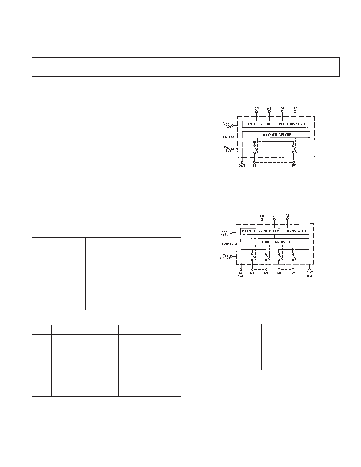
The AD7501 and AD7503 are monolithic CMOS, 8-channel
analog multiplexers which switch one of eight inputs to a
common
lines and an “enable” input. The AD7503 is identical to the
AD7501 except its “enable” logic is inverted. All digital inputs
are TTL/DTL and CMOS logic compatible.
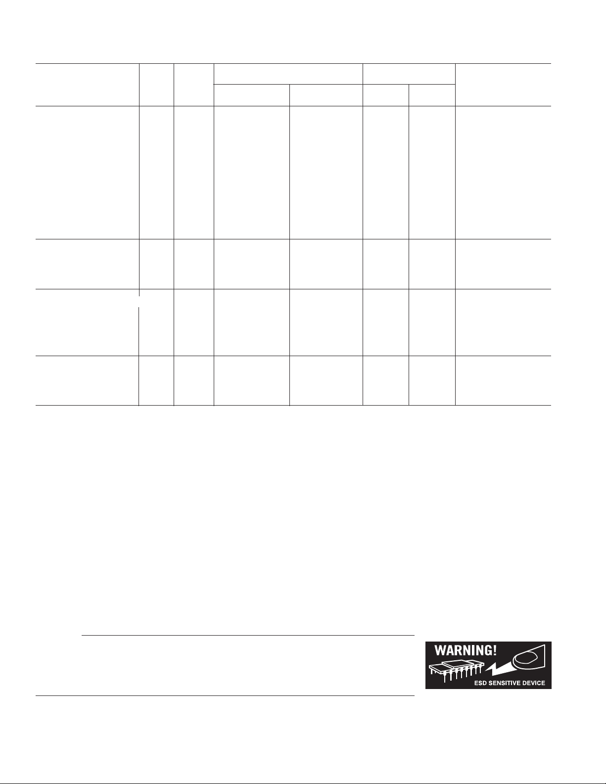
The AD7502 is a monolithic CMOS dual 4-channel analog
multiplexer. Depending on the state of two binary address
inputs and an “enable,” it switches two output buses to two
of eight inputs.
output, depending on the state of three binary address
Truth Tables
4-/8-Channel Analog Multiplexers
AD7501/AD7502/AD7503
FUNCTIONAL BLOCK DIAGRAM
AD7501/AD7503
AD7502
AD7501
A
2
00011
00112
01013
01114
10015
10116
11017
11118
XXX0None
A
2
00001
00102
01003
01104
10005
10106
11007
11108
XXX1None
A
1
A
1
A
0
AD7503
A
0
EN “ON”
EN “ON”
A
l
00 11 & 5
01 12 & 6
10 13 & 7
11 14 & 8
XX 0None
AD7502
A
0
EN “ON”
REV. B
Information furnished by Analog Devices is believed to be accurate and
reliable. However, no responsibility is assumed by Analog Devices for its
use, nor for any infringements of patents or other rights of third parties that
may result from its use. No license is granted by implication or otherwise
under any patent or patent rights of Analog Devices. Trademarks and
registered trademarks are the property of their respective companies.
One Technology Way, P.O. Box 9106, Norwood, MA 02062-9106, U.S.A.
Tel: 781/329-4700 www.analog.com
Fax: 781/326-8703 © 2003 Analog Devices, Inc. All rights reserved.
Page 2
AD7501/AD7502/AD7503–SPECIFICATIONS
@ +25°C Temperature Range
Parameter Version1Condition AD7501, AD7503 AD7502 AD7503 AD7502 Test Conditions
ANALOG SWITCH
R
ON
RON vs. V
S
R
vs. Temperature All ON 0.5%/°C typ 0.5%/°C typ VS = 0 V, IS = 1.0 mA
ON
∆R
Between Switches All ON 4% typ 4% typ
ON
R
vs. Temperature Between
ON
Switches All ON ± 0.01%/°C ± 0.01%/°C
I
S
I
OUT
|I
– IS|KON 12 nA max 7 nA max 300 nA max 175 nA max VS = 0
OUT
DIGITAL CONTROL
V
INL
V
INH
I
or I
INL
INH
C
IN
DYNAMIC CHARACTERISTICS
t
ON
t
OFF
C
S
C
OUT
C
SOUT
CSS Between Any Two Switches All OFF 0.5 pF typ 0.5 pF typ
POWER SUPPLY
I
DD
I
SS
I
DD
I
SS
NOTES
1
KN version specified for 0°C to +70°C, KQ version for –25°C to +85°C; and SQ, SE versions for –55°C to +125°C.
Specifications subject to change without notice.
All ON 170 Ω typ, 300 Ω max 170 Ω typ, 300 Ω max –10 V ≤ VS ≤ +10 V
All ON 20% typ 20% typ IS = 1.0 mA
K OFF 0.2 nA typ, 2 nA max 0.2 nA typ, 2 nA max 50 nA max 50 nA max VS = –10 V, V
S OFF 0.5 nA max 0.5 nA max 50 nA max 50 nA max VS = +10 V, V
K OFF 1 nA typ, 10 nA max 0.6 nA typ, 5 nA max 250 nA max 125 nA max VS = –10 V, V
S OFF 5 nA max 3 nA max 250 nA max 125 nA max AD7501/02: Enable LOW
SON5.5 nA max 3.5 nA max 300 nA max 175 nA max
All 0.8 V max 0.8 V max
All 2.4 V min 2.4 V min
All 10 nA typ 10 nA typ
All 3 pF typ 3 pF typ
All 0.8 µs typ 0.8 µs typ VIN = 0 to +5.0 V
All 0.8 µs typ 0.8 µs typ (See Test Circuit 2)
All OFF 5 pF typ 5 pF typ
All OFF 30 pF typ 15 pF typ
All OFF 0.5 pF typ 0.5 pF typ
All 500 µA max 500 µA max 500 µA max 500 µA max All Digital Inputs Low
All 500 µA max 500 µA max 500 µA max 500 µA max
All 800 µA max 800 µA max 800 µA max 800 µA max All Digital Inputs High
All 800 µA max 800 µA max 800 µA max 800 µA max
Switch AD7501,
(VDD = +15 V, VSS = –15 V unless otherwise noted.)
Over Specified
V
= +10 V, V
S
AD7503: Enable HIGH
= +10 V and
OUT
= –10 V
OUT
= +10 V and
OUT
= –10 V
OUT
ABSOLUTE MAXIMUM RATINGS
(TA = +25°C unless otherwise noted)
VDD to GND . . . . . . . . . . . . . . . . . . . . . . . . . . . . . . . . . +17 V
to GND . . . . . . . . . . . . . . . . . . . . . . . . . . . . . . . . . . –17 V
V
SS
V Between Any Switch Terminals
Digital Input Voltage Range . . . . . . . . . . . . . . . V
Overvoltage at V
(VS) . . . . . . . . . . . . . . . . . . . . . . VSS, V
OUT
1
. . . . . . . . . . . . . . . . . 25 V
to GND
DD
DD
Switch Current (IS, Continuous One Channel) . . . . . . .35 mA
Switch Current (I
, Surge One Channel)
S
1 ms Duration, 10% Duty Cycle . . . . . . . . . . . . . . . 50 mA
Power Dissipation (Any Package)
Up to +75°C . . . . . . . . . . . . . . . . . . . . . . . . . . . . . 450 mW
Operating Temperature
Commercial (KN Version) . . . . . . . . . . . . . . . 0°C to +70°C
Industrial (KQ Version) . . . . . . . . . . . . . . . –25°C to +85°C
Extended (SQ, SE Versions) . . . . . . . . . . –55°C to +125°C
Storage Temperature . . . . . . . . . . . . . . . . . . –65°C to +150°C
Lead Temperature (Soldering, 10 sec) . . . . . . . . . . . .+300°C
CAUTION
1
Do not apply voltages higher than VDD and VSS to any other terminal, especially
when VSS = VDD = 0 V all other pins should be at 0 V.
2
The digital control inputs are diode protected; however, permanent damage may
occur on unconnected units under high energy electrostatic fields. Keep unused
units in conductive foam at all times.
Derates above +75°C by . . . . . . . . . . . . . . . . . . . 6 mW/°C
CAUTION
ESD (electrostatic discharge) sensitive device. Electrostatic charges as high as 4000 V readily
accumulate on the human body and test equipment and can discharge without detection. Although the
AD7501, AD7502, and AD7503 feature proprietary ESD protection circuitry, permanent damage
may occur on devices subjected to high energy electrostatic discharges. Therefore, proper ESD
precautions are recommended to avoid performance degradation or loss of functionality.
–2–
REV. B
Page 3

AD7501/AD7502/AD7503
ORDERING GUIDE
Temperature Package
Range Options
2
Model
l
AD7501KN 0°C to +70°C N-16
AD7501KQ –25°C to +85°C Q-16
AD7501SQ –55°C to +125°C Q-16
AD7501SE –55°C to +125°C E-20A
AD7502KN 0°C to +70°C N-16
AD7502KQ –25°C to +85°C Q-16
AD7502SQ –55°C to +125°C Q-16
AD7502SE –55°C to +125°C E-20A
AD7503KN 0°C to +70°C N-16
AD7503KQ –25°C to +85°C Q-16
AD7503SQ –55°C to +125°C Q-16
AD7503SE –55°C to +125°C E-20A
NOTES
1
To order MIL-STD-883, Class B processed parts, add/883B to part number.
See the Analog Devices’ 1990 Military Databook for military data sheet.
2
E = LCC; N = PDIP; Q = CERDIP.
PIN CONFIGURATIONS
PDIP CERDIP
LCC
Typical Performance Characteristics
Figure 1a. RON vs. VS At Different Power
Supplies
Figure 2a. Digital Threshold Voltage
(V
, V
INH
INL
) vs. Power Supply
Figure 3. tON, t
Voltage
vs. Digital Input
OFF
Figure 1b. RON vs. VS At Different
Temperatures
Figure 2b. Digital Threshold Voltage
(V
, V
INH
) vs. Temperature
INL
–3–REV. B
Figure 4. Power Dissipation vs. Logic
Frequency (50% Duty Cycle)
Page 4

AD7501/AD7502/AD7503
TYPICAL SWITCHING CHARACTERISTICS
TEST CIRCUIT 1
1 µs/DIV
1 µs/DIV
OUTLINE DIMENSIONS
16-Lead Plastic Dual In-Line Package [PDIP]
(N-16)
Dimensions shown in inches and (millimeters)
0.785 (19.94)
0.765 (19.43)
0.745 (18.92)
16
1
0.100 (2.54)
BSC
0.015 (0.38)
0.180 (4.57)
MAX
0.150 (3.81)
0.130 (3.30)
0.110 (2.79)
0.022 (0.56)
0.018 (0.46)
0.014 (0.36)
CONTROLLING DIMENSIONS ARE IN INCHES; MILLIMETER DIMENSIONS
(IN PARENTHESES) ARE ROUNDED-OFF INCH EQUIVALENTS FOR
REFERENCE ONLY AND ARE NOT APPROPRIATE FOR USE IN DESIGN
COMPLIANT TO JEDEC STANDARDS MO-095AC
0.060 (1.52)
0.050 (1.27)
0.045 (1.14)
9
8
MIN
0.295 (7.49)
0.285 (7.24)
0.275 (6.99)
SEATING
PLANE
0.325 (8.26)
0.310 (7.87)
0.300 (7.62)
0.015 (0.38)
0.010 (0.25)
0.008 (0.20)
0.150 (3.81)
0.135 (3.43)
0.120 (3.05)
16-Lead Ceramic Dual In-Line Package [CERDIP]
(Q-16)
Dimensions shown in inches and (millimeters)
C01129-0-7/03(B)
TEST CIRCUIT 2
1 µs/DIV
1 µs/DIV
1 µs/DIV
0.005
(0.13)
MIN
0.200 (5.08)
MAX
0.200 (5.08)
0.125 (3.18)
0.023 (0.58)
0.014 (0.36)
CONTROLLING DIMENSIONS ARE IN INCHES; MILLIMETERS DIMENSIONS
(IN PARENTHESES) ARE ROUNDED-OFF INCH EQUIVALENTS FOR
REFERENCE ONLY AND ARE NOT APPROPRIATE FOR USE IN DESIGN
0.098 (2.49)
MAX
18
0.840 (21.34) MAX
0.070 (1.78)
0.100
(2.54)
0.030 (0.76)
BSC
PIN 1
16
9
0.310 (7.87)
0.220 (5.59)
0.060 (1.52)
0.015 (0.38)
0.150 (3.81)
MIN
SEATING
PLANE
15
0
20-Terminal Ceramic Leadless Chip Carrier [LCC]
(E-20A)
Dimensions shown in inches and (millimeters)
20
1
VIEW
0.150 (3.81)
BSC
0.200 (5.08)
REF
0.100 (2.54) REF
0.015 (0.38)
MIN
3
4
0.028 (0.71)
0.022 (0.56)
0.050 (1.27)
8
BSC
9
45 TYP
0.075 (1.91)
0.095 (2.41)
0.075 (1.90)
0.011 (0.28)
0.007 (0.18)
R TYP
0.075 (1.91)
REF
0.055 (1.40)
0.045 (1.14)
REF
19
18
14
13
BOTTOM
0.100 (2.54)
0.064 (1.63)
0.358 (9.09)
0.342 (8.69)
SQ
CONTROLLING DIMENSIONS ARE IN INCHES; MILLIMETERS DIMENSIONS
(IN PARENTHESES) ARE ROUNDED-OFF INCH EQUIVALENTS FOR
REFERENCE ONLY AND ARE NOT APPROPRIATE FOR USE IN DESIGN
0.358
(9.09)
MAX
0.088 (2.24)
0.054 (1.37)
SQ
0.320 (8.13)
0.290 (7.37)
0.015 (0.38)
0.008 (0.20)
–4–
REV. B
 Loading...