

Page 1
VOLTAGE
REFERENCE
TTL
INPUTS
8-BIT
BUS
INPUT
LATCHES
DAC
LATCHES
+5V
D7
D6
D5
D4
D3
D2
D1
D0
CONTROL LOGIC
TTL INPUTS
A3 A2 A1 A0
2.22k
+12V
10k
V
REFOUT
V
REFIN
CS WR
V
OUT3
V
OUT2
V
OUT1
V
OUT0
V
DD
V
SS
AGND
DGND
8 + 4-BIT
LATCHES
8 + 4-BIT
LATCHES
8 + 4-BIT
LATCHES
8 + 4-BIT
LATCHES
12-BIT
LATCH
–12V
12-BIT
DAC
12-BIT
DAC
12-BIT
DAC
12-BIT
DAC
12-BIT
LATCH
12-BIT
LATCH
12-BIT
LATCH
10k
10k
10k
AD75004
Quad 12-Bit
a
FEATURES
4 Complete 12-Bit D/A Functions
Double-Buffered Latches
Simultaneous Update of All DACs Possible
65 V Output Range
High Stability Bandgap Reference
Monolithic BiMOS Construction
Guaranteed Monotonic over Temperature
3/4 LSB Linearity Guaranteed over Temperature
4 ms max Settling Time to 0.01%
Operates with 612 V Supplies
Low Power: 720 mW max Including Reference
TTL/5 V CMOS Compatible Logic Inputs
8-Bit Microprocessor Interface
24-Pin PDIP or 28-Lead PLCC Package
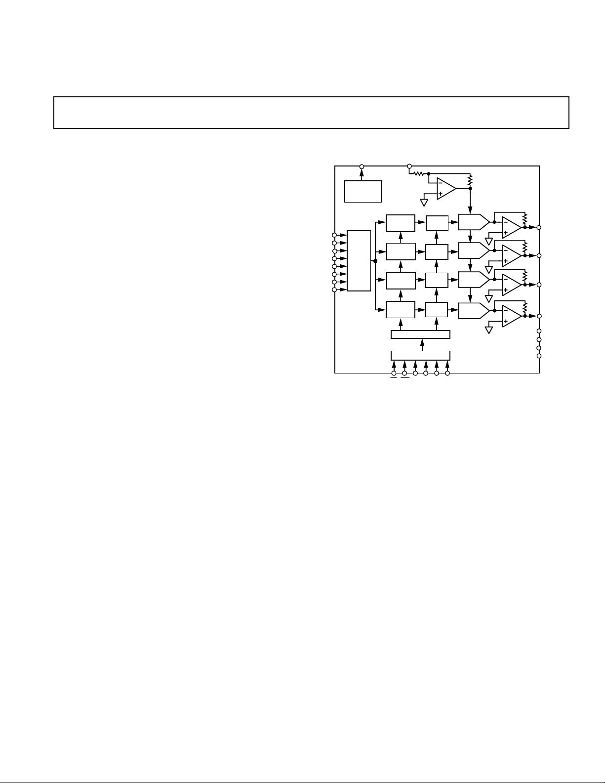
PRODUCT DESCRIPTION
The AD75004 contains four complete, voltage output, 12-bit
digital-to-analog converters, a high stability bandgap reference,
and double-buffered input latches on a single chip. The converters use 12 precision high speed bipolar current steering switches
and laser-trimmed thin-film resistor networks to provide fast
settling time and high accuracy.
Microprocessor compatibility is achieved by the on-chip
double-buffered latches. The design of the input latches allows
direct interface to 8-bit buses. The 12 bits of data from the first
rank of latches can then be transferred to the second rank,
avoiding generation of spurious analog output values. The latch
responds to strobe pulses as short as 50 ns, allowing use with
fast microprocessors.
The functional completeness and high performance of the
AD75004 results from a combination of advanced switch design, the BiMOS II fabrication process, and proven laser trimming technology. BiMOS II is an epitaxial BiCMOS process
optimized for analog and converter functions. The AD75004 is
trimmed at the wafer level and is specified to ± 1/2 LSB maximum linearity error at 25°C and ±3/4 LSB over the full operating temperature range. The on-chip output amplifiers provide
an output range of ±5 V, with 1 LSB equal to 2.44 mV.
REV. A
Information furnished by Analog Devices is believed to be accurate and
reliable. However, no responsibility is assumed by Analog Devices for its
use, nor for any infringements of patents or other rights of third parties
which may result from its use. No license is granted by implication or
otherwise under any patent or patent rights of Analog Devices.
D/A Converter
AD75004
FUNCTIONAL BLOCK DIAGRAM
The bandgap reference on the chip has low noise, long term
stability and temperature drift characteristics comparable to
discrete reference diodes. The absolute value of the reference is
laser trimmed to +5.00 V with 0.6% maximum error. Its temperature coefficient is also laser trimmed.
Typical full-scale gain TC is 15 ppm/°C. With guaranteed
monotonicity over the full temperature range, the AD75004 is
well suited for wide temperature range performance.
One Technology Way, P.O. Box 9106, Norwood, MA 02062-9106, U.S.A.
Tel: 617/329-4700 Fax: 617/326-8703
Page 2

AD75004–SPECIFICA TIONS
(TA = +258C, 612.0 V power supplies unless otherwise noted)
Parameter Symbol Min Typ Max Units
DIGITAL INPUTS (D0–D7, A0–A3, CS, WR)
Logic Levels (TTL Compatible)
Input Voltage, Logic “1” V
Input Voltage, Logic “0” V
Input Current, V
Input Current, V
= 5.5 V I
IH
= 0.8 V I
IL
Input Capacitance C
IH
IL
IH
IL
IN
2.0 5.5 V
0 0.8 V
10 µA
10 µA
10 pF
ACCURACY
Resolution 12 Bits
Integral Linearity Error ±1/4 61/2 LSB
Integral Linearity Error, T
MIN
to T
MAX
±1/2 ±3/4 LSB
Differential Linearity Error ±1/2 63/4 LSB
Differential Linearity Error, T
Gain (Full-Scale) Error
Gain Error Drift, T
Bipolar Zero Error
1
to T
MIN
1
Bipolar Zero Error Drift, T
MAX
MIN
MIN
1
to T
to T
MAX
MAX
1
Guaranteed Monotonic
±2 610 LSB
±15 ±30 ppm/°C
±1 62 LSB
±3 ±7 ppm/°C
CHANNEL-TO-CHANNEL MISMATCH
Integral Linearity Error ±1/2 61 LSB
Gain Error
Bipolar Zero Error
1
1
±1 64 LSB
±1 62 LSB
DYNAMIC PERFORMANCE
Settling Time to ±0.01% of FSR
for FSR Change, 2 kΩ || 500 pF Load 2 4 µs
Slew Rate, 2 kΩ || 500 pF Load 5 V/µs
Digital Input Crosstalk (Static)
2
–50 dB
ANALOG OUTPUTS
Full-Scale Range (FSR) V
Output Current I
OUT
OUT
±5mA
±5V
Short Circuit Limit Current 640 mA
VOLTAGE REFERENCE
Reference Output Voltage V
Temperature Coefficient ±15 ± 25 ppm/°C
Reference Output Currents
3
Reference Input Voltage V
Reference Input Current @ 5.0 V I
POWER SUPPLY GAIN SENSITIVITY
∆Gain/∆V
, VDD = +10.8 to +13.2 V dc
DD
∆Gain/∆VSS, VSS = –10.8 to –13.2 V dc
1
1
REFOUT
REFIN
REFIN
4.97 5.00 5.03 V
3.0 5.0 mA
4.5 5.0 5.5 V
3.0 mA
±15 625 ppm of FSR/%
±15 625 ppm of FSR/%
POWER SUPPLY REQUIREMENTS
Voltage Range V
Supply Currents IDD, I
DD
, V
SS
SS
610.8 ±12 613.2 V
±25 630 mA
TEMPERATURE RANGE
Specification T
MIN
, T
MAX
0 +70 °C
Storage –65 +150 °C
NOTES
1
Gain and bipolar zero errors are measured using internal voltage reference and include its errors.
2
Digital crosstalk is defined as the change in any one output’s steady state value as a result of any other output being driven from V
2 kΩ || 500 pF load by means of varying the digital input code.
3
The internal voltage reference is intended to drive on-chip only; buffer it if using it externally.
4
All minimum and maximum specifications are guaranteed, and specifications shown in boldface are tested on all production units at final electrical test. Results from
those tests are used to calculate outgoing quality levels.
Specifications subject to change without notice.
OUTMIN
to V
OUTMAX
into a
–2–
REV. A
Page 3

AD75004
WARNING!
ESD SENSITIVE DEVICE
TIMING CHARACTERISTICS
1
(TA = +258C, 612.0 V power supplies unless otherwise noted)
Parameter Symbol Min Units
Address Setup Time t
Address Hold Time t
Data Setup Time t
Data Hold Time t
Chip Select to Write Setup Time t
Write to Chip Select Hold Time t
Write Pulse Width t
NOTES
1
Timing measurement reference level is 1.5 V.
Specifications subject to change without notice
ADDRESS INPUTS
(A0–A3)
DATA INPUTS
(D0–D7)
CHIP SELECT
(CS)
WRITE
(WR)
t
1
1
2
3
4
5
6
7
t
5
t
t
7
t
2
t
3
4
30 ns
10 ns
10 ns
45 ns
0ns
0ns
50 ns
t
6
ABSOLUTE MAXIMUM RATINGS*
(TA = +25°C unless otherwise noted)
Min Max Units Conditions
TRUTH TABLE
Control and Address Lines
CS WR A3 A2 A1 A0 Operation
1 X X X X X No operation
X 1 X X X X No operation
0 0 0 0 A1* A0* 8 LSBs → one input latch
0 0 0 1 A1* A0* 4 MSBs → one input latch
0 0 1 0 A1* A0* Update one DAC latch
0 0 1 1 X X Update all 4 DAC latches
NOTE
*The A1 and A0 inputs specify the relevant channel.
A1 A0 Channel
000
011
102
113
V
to DGND –0.3 +18 V
DD
V
to DGND –18 +0.3 V
SS
V
to V
DD
V
SS
to AGND –0.3 V
REFIN
Digital Inputs to DGND –0.3 V
–0.3 +26.4 V
DD
DD
V
V
AGND to DGND –0.3 +0.3 V
Short to AGND on Analog Outputs Indefinite sec
Power Dissipation 1.0 W T
≤ 75°C
A
Specification Temperature Range 0 +70 °C
Storage Temperature –65 +150 °C
Lead Temperature +300 °C Soldering, 10 seconds
*Stresses above those listed under “Absolute Maximum Ratings” may cause permanent damage to the device. These are stress
ratings only and functional operation of the device at these or any other conditions above those indicated in the operational
sections of this specification is not implied. Exposure to absolute maximum rating conditions for extended periods may affect
device reliability.
CAUTION
ESD (electrostatic discharge) sensitive device. Electrostatic charges as high as 4000 V readily
accumulate on the human body and test equipment and can discharge without detection.
Although the AD75004 features proprietary ESD protection circuitry, permanent damage may
occur on devices subjected to high energy electrostatic discharges. Therefore, proper ESD
precautions are recommended to avoid performance degradation or loss of functionality.
ORDERING GUIDE
Model Temperature Range Package Option*
AD75004KN 0°C to +70°C N-24A
AD75004KP 0°C to +70°C P-28A
*N = Plastic DIP; P = Plastic Leaded Chip Carrier.
REV. A
–3–
Page 4

AD75004
WR
A2
D7
D6
D5
D4
D3
D2
D1
D0
A3
CS
AGND
DGND
A0
A1
V
DD
OUT3
V
V
OUT2
OUT0
V
OUT1
V
REFIN
V
V
SS
REFOUT
V
1
2
3
7
24
23
22
18
8
9
10
17
16
15
11
12
14
13
4
5
21
20
6
19
TOP VIEW
(Not to Scale)
AD75004KN
AD75004KP
TOP VIEW
(Not to Scale)
5
6
7
8
9
10
11
28 27 261234
25
24
23
22
21
20
19
12 13 14 15 16 17 18
D7
D6
D5
D4
D3
D2
D1
D0
WR
A2
A3
CS
AGND
DGND
A0
A1
V
DD
V
OUT3
V
OUT1
V
SS
NC
NC
NC
NC
NC = NO CONNECT
V
OUT2
V
OUT0
V
REFIN
V
REFOUT
4
PIN 1
IDENTIFIER
5
26
25
11
12
19
18
TOP VIEW
(PINS DOWN)
0.495 (12.57)
0.485 (12.32)
SQ
0.456 (11.58)
0.450 (11.43)
SQ
0.048 (1.21)
0.042 (1.07)
0.048 (1.21)
0.042 (1.07)
0.020
(0.50)
R
0.050
(1.27)
BSC
0.021 (0.53)
0.013 (0.33)
0.430 (10.92)
0.390 (9.91)
0.032 (0.81)
0.026 (0.66)
0.180 (4.57)
0.165 (4.19)
0.040 (1.01)
0.025 (0.64)
0.056 (1.42)
0.042 (1.07)
0.025 (0.63)
0.015 (0.38)
0.110 (2.79)
0.085 (2.16)
PIN DESCRIPTIONS
Plastic
PLCC DIP
Pin Pin Name Description
1 1 D7 Data Input Bit 7
2 2 D6 Data Input Bit 6
3 3 D5 Data Input Bit 5
5 4 D4 Data Input Bit 4
6 5 D3 Data Input Bit 3 or 11 (MSB)
7 6 D2 Data Input Bit 2 or 10
9 7 D1 Data Input Bit 1 or 9
10 8 D0 Data Input Bit 0 (LSB) or 8
11 9
13 10
CS Chip Select Input; Active Low
WR Write Input; Active Low
14 11 A3 Address Input Bit 3 (MSB)
15 12 A2 Address Input Bit 2
16 13 A1 Address Input Bit 1
17 14 A0 Address Input Bit 0 (LSB)
18 15 DGND Digital Ground
19 16 AGND Analog Ground
20 17 V
21 18 V
22 19 V
23 20 V
24 21 V
26 22 V
27 23 V
28 24 V
SS
REFOUT
REFIN
OUT0
OUT1
OUT2
OUT3
DD
–12 V Power Supply
+5 V Reference Output
Reference Input
Analog Output 0
Analog Output 1
Analog Output 2
Analog Output 3
+12 V Power Supply
4 – NC No Internal Connection
8 – NC No Internal Connection
12 – NC No Internal Connection
25 – NC No Internal Connection
PIN CONFIGURATIONS
24-Pin Plastic DIP
C1389a–5–10/91
28-Pin PLCC
Twos Complement Analog Output
Value in DAC Latch Voltage
MSB LSB
0111 1111 1111 (2047/2048) * V
0000 0000 0001 (1/2048) * V
0000 0000 0000 0 V
1111 1111 1111 – (1/2048) * V
1000 0000 0000 –V
24
0.2
(5.08)
MAX
0.175 (4.45)
0.12 (3.05)
112
PIN 1
0.02 (0.508)
0.015 (0.381)
BINARY CODE TABLE
Plastic DIP (N-24A) PLCC (P-28A)
1.290 (32.77)
1.150 (29.21)
0.100
(2.54)
BSC
0.060 (1.52)
0.015 (0.38)
0.065 (1.66)
0.45 (1.15)
REFIN
13
0.55 (13.97)
0.53 (13.47)
0.150
(3.81)
MIN
SEATING
PLANE
REFIN
REFIN
REFIN
OUTLINE DIMENSIONS
Dimensions shown in inches and (mm).
0.606 (15.4)
0.594 (15.09)
0.16 (4.07)
0.14 (3.56)
0.012 (0.305)
0.008 (0.203)
–4–
PRINTED IN U.S.A.
REV. A
 Loading...