

Page 1
a
A
781/461-3113
2010
1 MSPS, Serial 14-Bit SAR ADC
AD7485
FEATURES
Fast Throughput Rate: 1 MSPS
Wide Input Bandwidth: 40 MHz
Excellent DC Accuracy Performance
Flexible Serial Interface
Low Power:
80 mW (Full Power) and 3 mW (NAP Mode)
STANDBY Mode: 2 A Max
Single 5 V Supply Operation
Internal 2.5 V Reference
Full-Scale Overrange Indication
GENERAL DESCRIPTION
The AD7485 is a 14-bit, high speed, low power, successiveapproximation ADC. The part features a serial interface with
throughput rates up to 1 MSPS. The part contains a low noise,
wide bandwidth track-and-hold that can handle input frequencies
in excess of 40 MHz.
The conversion process is a proprietary algorithmic successiveapproximation technique. The input signal is sampled and a
conversion is initiated on the falling edge of the CONVST signal.
The conversion process is controlled by an external master
clock. Interfacing is via standard serial signal lines, making the
part directly compatible with microcontrollers and DSPs.
The AD7485 provides excellent ac and dc performance specifications. Factory trimming ensures high dc accuracy resulting in
very low INL, DNL, offset, and gain errors.
The part uses advanced design techniques to achieve very low
power dissipation at high throughput rates. Power consumption
in the normal mode of operation is 80 mW. There are two powersaving modes: a NAP mode keeps reference circuitry alive for
quick power-up and consumes 3 mW, while a STANDBY mode
reduces power consumption to a mere 10 µW.
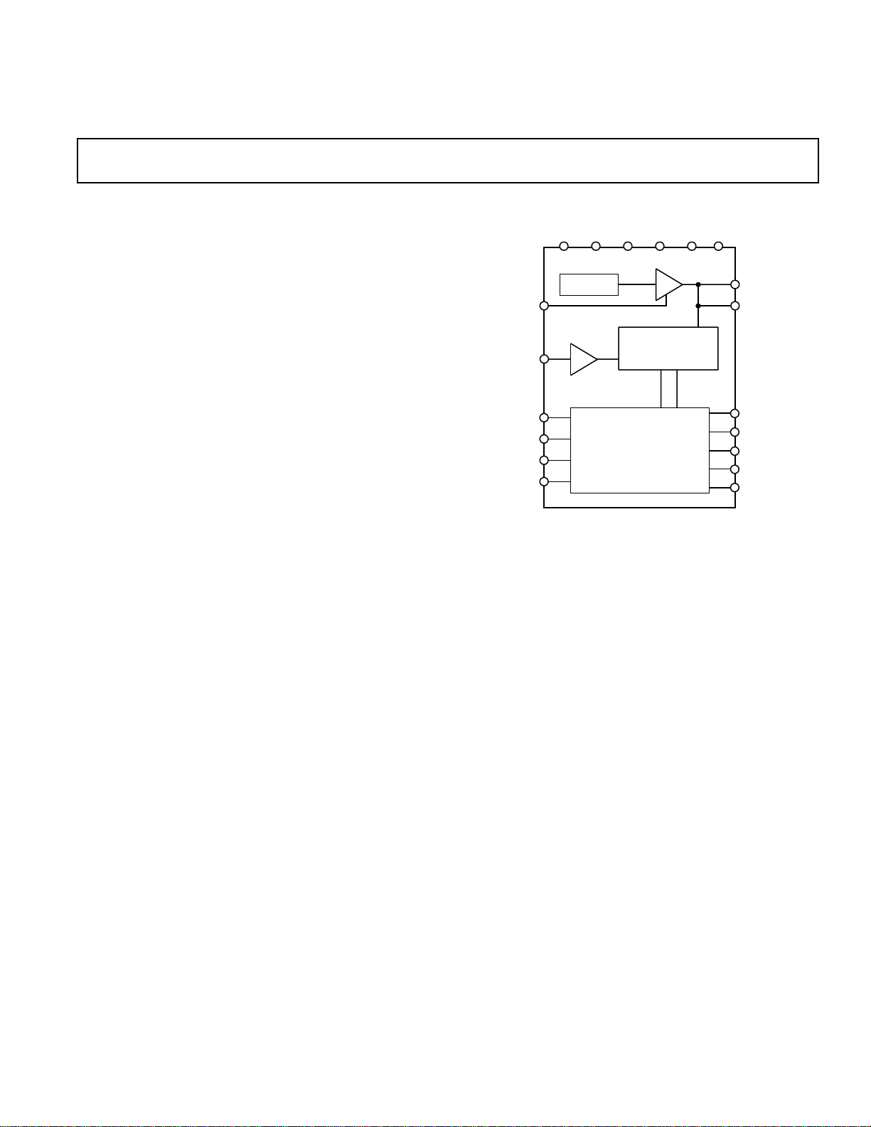
FUNCTIONAL BLOCK DIAGRAM
REFSEL
VIN
NAP
STBY
RESET
CONVST
AVDDAGND C
2.5 V
REFERENCE
T/H
AD7485
LOGIC AND I/O
BIASDVDD
ALGORITHMIC
CONTROL
REGISTERS
BUF
14-BIT
SAR
V
DRIVE
DGND
REFOUT
REFIN
MCLK
TFS
SCO
SDO
SMODE
The AD7485 features an on-board 2.5 V reference, but the part can
also accommodate an externally provided 2.5 V reference source.
The nominal analog input range is 0 V to 2.5 V.
The AD7485 also provides the user with overrange indication via a
fifteenth bit. If the analog input range strays outside the 0 V to
2.5 V input range, the fifteenth data bit is set to a logic high.
The AD7485 is powered from a 4.75 V to 5.25 V supply. The
part also provides a V
pin that allows the user to set the
DRIVE
voltage levels for the digital interface lines. The range for this
V
pin is from 2.7 V to 5.25 V. The part is housed in a
DRIVE
48-lead LQFP package and is specified over a –40°C to +85°C
temperature range.
REV.
Information furnished by Analog Devices is believed to be accurate and
reliable. However, no responsibility is assumed by Analog Devices for its
use, nor for any infringements of patents or other rights of third parties that
may result from its use. No license is granted by implication or otherwise
under any patent or patent rights of Analog Devices.
One Technology Way, P.O. Box 9106, Norwood, MA 02062-9106, U.S.A.
Tel: 781/329-4700 www.analog.com
Fax: © Analog Devices, Inc.,
Page 2

AD7485–SPECIFICATIONS
A
(VDD = 5 V 5%, AGND = DGND = 0 V, V
1
tions T
MIN
to T
MAX
and valid for V
DRIVE
= External, f
REF
= 1 MSPS; all specifica-
SAMPLE
= 2.7 V to 5.25 V, unless otherwise noted.)
Parameter Specification Unit Test Conditions/Comments
DYNAMIC PERFORMANCE
2, 3
Signal to Noise + Distortion (SINAD)
4
76.5 dB min
fIN = 500 kHz Sine Wave
78 dB typ
Total Harmonic Distortion (THD)
4
77 dB typ Internal Reference
–90 dB max
–95 dB typ
–92 dB typ Internal Reference
Peak Harmonic or Spurious Noise (SFDR)
Intermodulation Distortion (IMD)
4
Second-Order Terms –96 dB typ f
4
–88 dB max
= 95.053 kHz, f
IN1
= 105.329 kHz
IN2
Third-Order Terms –94 dB typ
Aperture Delay 10 ns typ
Full Power Bandwidth 40 MHz typ @ 3 dB
3.5 MHz typ @ 0.1 dB
DC ACCURACY
Resolution 14 Bits
Integral Nonlinearity
Differential Nonlinearity
Offset Error
Gain Error
4
4
4
4
± 1LSB max
± 0.5 LSB typ
± 0.75 LSB max Guaranteed No Missed Codes to 14 Bits
± 0.25 LSB typ
± 6LSB max
0.036 %FSR max
± 6LSB max
0.036 %FSR max
ANALOG INPUT
Input Voltage 0 V min
2.5 V max
DC Leakage Current ± 1 µA max
Input Capacitance
5
35 pF typ
REFERENCE INPUT/OUTPUT
V
Input Voltage 2.5 V ± 1% for Specified Performance
REFIN
V
Input DC Leakage Current ± 1 µA max
REFIN
V
Input Capacitance
REFIN
V
Input Current
REFIN
V
V
V
V
Output Voltage 2.5 V typ
REFOUT
Error @ 25°C ± 50 mV typ
REFOUT
Error T
REFOUT
Output Impedance 1 Ω typ
REFOUT
MIN
6
to T
5
MAX
25 pF typ
220 A typ External Reference
± 100 mV max
LOGIC INPUTS
Input High Voltage, V
Input Low Voltage, V
Input Current, I
Input Capacitance, C
LOGIC OUTPUTS
Output High Voltage, V
Output Low Voltage, V
Floating-State Leakage Current ± 10 µA max
Floating-State Output Capacitance
INH
INL
IN
5
IN
7
OH
7
OL
5
V
–1V min
DRIVE
0.4 V max
± 1 µA max
10 pF typ
0.7 × V
0.3 × V
DRIVE
DRIVE
V min
V max
10 pF max
Output Coding Straight (Natural) Binary
CONVERSION RATE
Conversion Time 24 MCLKs
Track/Hold Acquisition Time 100 ns max Sine Wave Input
70 ns max Full-Scale Step Input
Throughput Rate 1 MSPS max
REV. –2–
Page 3
Parameter Specification Unit Test Conditions/Comments
131785
A
POWER REQUIREMENTS
V
DD
V
DRIVE
5V± 5%
2.7 V min
5.25 V max
I
DD
Normal Mode (Static) mA max
Normal Mode (Operational) mA max
NAP Mode 0.6 mA max
STANDBY Mode
8
2 µA max
0.5 µA typ
Power Dissipation
Normal Mode (Operational) mW max
NAP Mode 3 mW max
STANDBY Mode
NOTES
1
Temperature ranges as follows: –40°C to +85°C.
2
SINAD figures quoted include external analog input circuit noise contribution of approximately 1 dB.
3
See Typical Performance Characteristics section for analog input circuits used.
4
See Terminology.
5
Sample tested @ 25°C to ensure compliance.
6
Current drawn from external reference during conversion.
7
I
= 200 µA.
LOAD
8
Digital input levels at GND or V
Specifications subject to change without notice.
8
.
DRIVE
10 µW max
AD7485
TIMING CHARACTERISTICS
(VDD = 5 V 5%, AGND = DGND = 0 V, V
1
valid for V
= 2.7 V to 5.25 V, unless otherwise noted.)
DRIVE
= External; all specifications T
REF
MIN
to T
MAX
and
Parameter Symbol Min Typ Max Unit
Master Clock Frequency f
MCLK Period t
Conversion Time t
CONVST Low Period (Mode 1)
CONVST High Period (Mode 1)
2
2
MCLK High Period t
MCLK Low Period t
CONVST Falling Edge to MCLK Rising Edge t
MCLK Rising Edge to MSB Valid t
Data Valid before SCO Falling Edge t
Data Valid after SCO Falling Edge t
CONVST Rising Edge to SDO Three-State t
CONVST Low Period (Mode 2)
CONVST High Period (Mode 2)
2
3
CONVST Falling Edge to TFS Falling Edge t
TFS Falling Edge to MSB Valid t
TFS Rising Edge to SDO Three-State t
TFS Low Period
TFS High Period
4
4
MCLK Fall Time t
MCLK Rise Time t
MCLK – SCO Delay t
NOTES
1
All timing specifications given above are with a 25 pF load capacitance. With a load capacitance greater than this value, a digital buffer or latch must be used.
2
CONVST idling high. See Serial Interface section for further details.
3
CONVST idling low. See Serial Interface section for further details.
4
TFS can also be tied low in this mode.
Specifications subject to change without notice.
MCLK
1
2
t
3
t
4
5
6
7
8
9
10
11
t
12
t
13
14
15
16
t
17
t
18
19
20
21
0.01 25 MHz
40 100000 ns
t1 24 ns
t1 22 ns
10 ns
0.4 t
0.4 t
1
1
0.6 t
0.6 t
1
1
ns
ns
7ns
15 ns
10 ns
20 ns
6ns
10 t1 2ns
10 ns
10 ns
30 ns
8ns
t1 22 ns
10 ns
525ns
525ns
625ns
REV.
–3–
Page 4
AD7485
A
ABSOLUTE MAXIMUM RATINGS*
(TA = 25°C, unless otherwise noted.)
VDD to GND . . . . . . . . . . . . . . . . . . . . . . . . . . –0.3 V to +7 V
V
to GND . . . . . . . . . . . . . . . . . . . . . . . . –0.3 V to +7 V
DRIVE
Analog Input Voltage to GND . . . . . . –0.3 V to AV
Digital Input Voltage to GND . . . . . –0.3 V to V
REFIN to GND . . . . . . . . . . . . . . . . –0.3 V to AV
DD
DRIVE
DD
+ 0.3 V
+ 0.3 V
+ 0.3 V
Input Current to Any Pin except Supplies . . . . . . . . . ±10 mA
Operating Temperature Range
Commercial . . . . . . . . . . . . . . . . . . . . . . . . –40°C to +85°C
Storage Temperature Range . . . . . . . . . . . . –65°C to +150°C
Junction Temperature . . . . . . . . . . . . . . . . . . . . . . . . . 150°C
JA Thermal Impedance . . . . . . . . . . . . . . . . . . . . . . . 50°C/W
Thermal Impedance . . . . . . . . . . . . . . . . . . . . . . . 10°C/W
JC
Lead Temperature, Soldering
Vapor Phase (60 sec) . . . . . . . . . . . . . . . . . . . . . . . . 215°C
Infrared (15 sec) . . . . . . . . . . . . . . . . . . . . . . . . . . . 220°C
ESD . . . . . . . . . . . . . . . . . . . . . . . . . . . . . . . . . . . . . . . . . 1 kV
*Stresses above those listed under Absolute Maximum Ratings may cause perma-
nent damage to the device. This is a stress rating only; functional operation of the
device at these or any other conditions above those listed in the operational sections
of this specification is not implied. Exposure to absolute maximum rating conditions for extended periods may affect device reliability.
CAUTION
ESD (electrostatic discharge) sensitive device. Electrostatic charges as high as 4000 V readily accumulate
on the human body and test equipment and can discharge without detection. Although the AD7485
features proprietary ESD protection circuitry, permanent damage may occur on devices subjected to
high energy electrostatic discharges. Therefore, proper ESD precautions are recommended to avoid
performance degradation or loss of functionality.
PIN CONFIGURATION
AGND
AGND
AVDDDVDDDGND
DGND
RESET
CONVST
SCO
DGND
DGND
SDO
DGND
DGND
DGND
36
35
34
33
32
31
30
29
28
27
26
25
DGND
SMODE
TFS
DGND
DGND
V
DRIVE
DGND
DGND
DV
DD
DGND
DGND
DGND
DGND
AV
C
BIAS
AGND
AGND
AV
AGND
VIN
REFOUT
REFIN
REFSEL
AGND
AGND
48 47 46 45 44 39 38 3743 42 41 40
1
DD
PIN 1
2
IDENTIFIER
3
4
5
DD
6
7
8
9
10
11
12
13 14 15 16 17 18 19 20 21 22 23 24
DD
AV
AGND
AGND
AD7485
TOP VIEW
(Not to Scale)
NAP
STBY
MCLK
DGND
DGND
WARNING!
ESD SENSITIVE DEVICE
REV. –4–
Page 5

AD7485
A
PIN FUNCTION DESCRIPTIONS
Pin
No. Mnemonic Description
1, 5, 13, 46 AV
2C
DD
BIAS
3, 4, 6, 11, 12, AGND Power Supply Ground for Analog Circuitry
14, 15, 47, 48
7VIN Analog Input. Single-ended analog input channel.
8 REFOUT Reference Output. REFOUT connects to the output of the internal 2.5 V reference buffer. A 470 nF
9 REFIN Reference Input. A 470 nF capacitor must be placed between this pin and AGND. When using
10 REFSEL Reference Decoupling Pin. When using the internal reference, a 1 nF capacitor must be connected
16 STBY Standby Logic Input. When this pin is logic high, the device will be placed in STANDBY mode.
17 NAP Nap Logic Input. When this pin is logic high, the device will be placed in a very low power mode.
18 MCLK
19, 20, 22–28 DGND Ground Reference for Digital Circuitry
30, 31, 33, 34
37–39, 43, 44
21 SDO Serial Data Output. The conversion data is latched out on this pin on the rising edge of SCO. It
29, 45 DV
32 V
DD
DRIVE
35 TFS Transmit Frame Sync Input. In Serial Mode 2, this pin acts as a framing signal for the serial data
36 SMODE Serial Mode Input. A logic low on this pin selects Serial Mode 1 and a logic high selects Serial
40 SCO Serial Clock Output. This clock is derived from MCLK and is used to latch conversion data from
41 CONVST
42 RESET Reset Logic Input. A falling edge on this pin resets the internal state machine and terminates a
Positive Power Supply for Analog Circuitry
Decoupling Pin for Internal Bias Voltage. A 1 nF capacitor should be placed between this pin
and AGND.
capacitor must be placed between this pin and AGND.
an external voltage reference source, the reference voltage should be applied to this pin.
from this pin to AGND. When using an external reference source, this pin should be connected
directly to AGND.
See the Power Saving section for further details.
See the Power Saving section for further details.
Master Clock Input. This is the input for the master clock, which controls the conversion cycle. The fre-
quency of this clock may be up to 25 MHz. Twenty-four clock cycles are required for each conversion.
should be latched into the receiving serial port of the DSP on the falling edge of SCO. The overrange bit is latched out first, then 14 bits of data (MSB first) followed by a trailing zero.
Positive Power Supply for Digital Circuitry
Logic Power Supply Input. The voltage supplied at this pin determines at what voltage the interface
logic of the AD7485 will operate.
being clocked out on SDO. A falling edge on TFS brings SDO out of three-state and the data starts
to get clocked out on the next rising edge of SCO.
Mode 2. See the Serial Interface section for further details.
the device. See the Serial Interface section for further details.
Convert Start Logic Input. A conversion is initiated on the falling edge of the CONVST signal. The
input track/hold amplifier goes from track mode to hold mode and the conversion process commences.
conversion that may be in progress. Holding this pin low keeps the part in a reset state.
REV.
–5–
Page 6

AD7485
A
TERMINOLOGY
Integral Nonlinearity
This is the maximum deviation from a straight line passing
through the endpoints of the ADC transfer function. The endpoints of the transfer function are zero scale, a point 1/2 LSB
below the first code transition, and full scale, a point 1/2 LSB
above the last code transition.
Differential Nonlinearity
This is the difference between the measured and the ideal
1 LSB change between any two adjacent codes in the ADC.
Offset Error
This is the deviation of the first code transition (00 . . . 000) to
(00 . . . 001) from the ideal, i.e., AGND + 0.5 LSB.
Gain Error
This is the deviation of the last code transition (111 . . . 110) to
(111 . . . 111) from the ideal (i.e., V
– 1.5 LSB) after the
REF
offset error has been adjusted out.
Track/Hold Acquisition Time
Track/hold acquisition time is the time required for the output
of the track/hold amplifier to reach its final value, within ±1/2 LSB,
after the end of conversion (the point at which the track/hold
returns to track mode).
Signal to (Noise + Distortion) Ratio
This is the measured ratio of signal to (noise + distortion) at
the output of the A/D converter. The signal is the rms amplitude
of the fundamental. Noise is the sum of all nonfundamental
signals up to half the sampling frequency (f
/2), excluding dc.
S
The ratio is dependent on the number of quantization levels in
the digitization process; the more levels, the smaller the quantization noise. The theoretical signal to (noise + distortion) ratio
for an ideal N-bit converter with a sine wave input is given by:
Signal to Noise Distortion N dB()..+=+
602 176
()
Thus, for a 14-bit converter this is 86.04 dB.
Total Harmonic Distortion
Total harmonic distortion (THD) is the ratio of the rms sum
of the harmonics to the fundamental. For the AD7485, it is
defined as:
VVVVV
++++
THD dB log
where V1 is the rms amplitude of the fundamental and V2, V3,
V
, V5, and V6 are the rms amplitudes of the second through
4
=
20
()
223242526
V
1
2
sixth harmonics.
Peak Harmonic or Spurious Noise
Peak harmonic or spurious noise is defined as the ratio of the
rms value of the next largest component in the ADC output
spectrum (up to f
/2 and excluding dc) to the rms value of the
S
fundamental. Normally, the value of this specification is determined by the largest harmonic in the spectrum, but for ADCs
where the harmonics are buried in the noise floor, it will be a
noise peak.
Intermodulation Distortion
With inputs consisting of sine waves at two frequencies, fa and fb,
any active device with nonlinearities will create distortion products
at sum and difference frequencies of mfa ± nfb where m, n = 0, 1, 2,
3, and so on. Intermodulation distortion terms are those for which
neither m nor n is equal to zero. For example, the second-order
terms include (fa + fb) and (fa – fb), while the third-order terms
include (2fa + fb), (2fa – fb), (fa + 2fb), and (fa – 2fb).
The AD7485 is tested using the CCIF standard where two
input frequencies near the top end of the input bandwidth are
used. In this case, the second-order terms are usually distanced
in frequency from the original sine waves while the third-order
terms are usually at a frequency close to the input frequencies.
As a result, the second- and third-order terms are specified
separately. The calculation of the intermodulation distortion
is as per the THD specification where it is the ratio of the rms
sum of the individual distortion products to the rms amplitude
of the sum of the fundamentals expressed in dBs.
REV. –6–
Page 7
1.0
INPUT FREQUENCY – kHz
100
THD – dB
–60
–100
1000 10000
–40
–80
–90
–70
–50
100
51
10
0
FREQUENCY – kHz
10
PSRR – dB
–20
–60
100 1000
0
–40
–50
–30
–10
–80
–70
100mV p-p SINE WAVE ON SUPPLY PINS
TEMPERATURE – C
–55
REFOUT – V
–0.0004
35 125
0.0004
–0.0008
–0.0012
0
–0.0020
–0.0016
–25 5 65 95
A
0.8
0.6
0.4
0.2
0
DNL – LSB
–0.2
–0.4
–0.6
–0.8
–1.0
0
1.0
0.8
0.6
0.4
0.2
0
INL – LSB
–0.2
–0.4
–0.6
–0.8
–1.0
0
Typical Performance Characteristics–AD7485
4096 8192 12288 16384
ADC CODE
TPC 1. Typical DNL
4096 8192 12288 16384
ADC CODE
TPC 4. THD vs. Input Tone for Different Input Resistances
SINAD – dB
TPC 3. SINAD vs. Input Tone (AD8021 Input Circuit)
REV.
TPC 2. Typical INL
80
75
70
65
10
100 1000 10000
INPUT FREQUENCY – kHz
TPC 5. PSRR without Decoupling
TPC 6. Reference Error
–7–
Page 8

AD7485
A
0
–20
–40
–60
dB
–80
–100
–120
–140
0 300100 200 400 500
FREQUENCY – kHz
f
= 10.7kHz
IN
SNR = 78.76dB
SNR + D = 78.70dB
THD = –97.10dB
TPC 7. 64k FFT Plot with 10 kHz Input Tone
+V
S
SIGNAL
BIAS
VOLTA G E
1k
AC
100
1k
3
2
150
8
+
AD829
–
1
5
7
220pF
V
6
4
–V
S
IN
Figure 1. Analog Input Circuit Used for 10 kHz Input Tone
+V
S
SIGNAL
BIAS
VOLTA G E
50
AC
220
2
3
8
+
AD8021
–
1
220
10pF
5
7
10pF
V
6
4
–V
S
IN
Figure 2. Analog Input Circuit Used for 500 kHz Input Tone
0
f
= 507.3kHz
IN
SNR = 78.35dB
–20
SNR + D = 78.33dB
THD = –100.33dB
–40
–60
dB
–80
–100
–120
–140
0 300100 200 400 500
FREQUENCY – kHz
TPC 8. 64k FFT Plot with 500 kHz Input Tone
Figure 1 shows the analog input circuit used to obtain the data
for the FFT plot shown in TPC 7. The circuit uses an Analog
Devices AD829 op amp as the input buffer. A bipolar analog
signal is applied as shown and biased up with a stable, low noise
dc voltage connected to the labeled terminal shown. A 220 pF
compensation capacitor is connected between Pin 5 of the AD829
and the analog ground plane. The AD829 is supplied with +12 V
and –12 V supplies. The supply pins are decoupled as close to
the device as possible, with both a 0.1 µF and 10 µF capacitor
connected to each pin. In each case, the 0.1 µF capacitor should be
the closer of the two capacitors to the device. More information
on the AD829 is available on the Analog Devices website.
For higher input bandwidth applications, Analog Devices’ AD8021
op amp (also available as a dual AD8022) is the recommended
choice to drive the AD7485. Figure 2 shows the analog input
circuit used to obtain the data for the FFT plot shown in TPC 8.
A bipolar analog signal is applied to the terminal shown and
biased with a stable, low noise dc voltage connected as shown. A
10 pF compensation capacitor is connected between Pin 5 of the
AD8021 and the negative supply. As with the previous circuit,
the AD8021 is supplied with +12 V and –12 V supplies. The
supply pins are decoupled as close to the device as possible with
both a 0.1 µF and 10 µF capacitor connected to each pin. In each
case, the 0.1 µF capacitor should be the closer of the two capaci-
tors to the device. The AD8021 Logic Reference pin is tied to
analog ground and the DISABLE pin is tied to the positive supply as shown. Detailed information on the AD8021 is available
on the Analog Devices website.
REV. –8–
Page 9

AD7485
A
CIRCUIT DESCRIPTION
CONVERTER OPERATION
The AD7485 is a 14-bit algorithmic successive-approximation
analog-to-digital converter based around a capacitive DAC. It provides the user with track-and-hold, reference, an A/D converter,
and versatile interface logic functions on a single chip. The analog
input signal range that the AD7485 can convert is 0 V to 2.5 V.
The part requires a 2.5 V reference that can be provided from
the part’s own internal reference or an external reference source.
Figure 3 shows a very simplified schematic of the ADC. The
Control Logic, SAR, and Capacitive DAC are used to add and
subtract fixed amounts of charge from the sampling capacitor to
bring the comparator back to a balanced condition.
COMPARATOR
CAPACITIVE
DAC
V
IN
REF
SWITCHES
SAR
CONTROL
LOGIC
OUTPUT DATA
14-BIT SERIAL
V
CONTROL
INPUTS
Figure 3. Simplified Block Diagram
Conversion is initiated on the AD7485 by pulsing the CONVST
input. On the falling edge of CONVST, the track/hold goes from
track to hold mode and the conversion sequence is started.
Conversion time for the part is 24 MCLK periods. Figure 4 shows
the ADC during conversion. When conversion starts, SW2 will
open and SW1 will move to position B causing the comparator to
become unbalanced. The ADC then runs through its successive
approximation routine and brings the comparator back into a
balanced condition. When the comparator is rebalanced, the
conversion result is available in the SAR register.
CAPACITIVE
DAC
A
V
AGND
IN
SW1
B
SW2
+
–
COMPARATOR
CONTROL LOGIC
Figure 4. ADC Conversion Phase
At the end of conversion, track-and-hold returns to tracking
mode and the acquisition time begins. The track/hold acquisition
time is 70 ns. Figure 5 shows the ADC during its acquisition
phase. SW2 is closed and SW1 is in position A. The comparator
is held in a balanced condition and the sampling capacitor acquires
the signal on V
.
IN
CAPACITIVE
DAC
V
AGND
A
IN
SW1
B
SW2
+
–
COMPARATOR
CONTROL LOGIC
Figure 5. ADC Acquisition Phase
ADC TRANSFER FUNCTION
The output coding of the AD7485 is straight binary. The designed
code transitions occur midway between successive integer LSB
values (i.e., 1/2 LSB, 3/2 LSB, and so on). The LSB size is
V
/16384. The nominal transfer characteristic for the
REF
AD7485 is shown in Figure 6.
111...111
111...110
111...000
011...111
ADC CODE
000...010
000...001
000...000
0V
0.5LSB
1LSB = V
ANALOG INPUT
+V
REF
/16384
REF
–1.5LSB
Figure 6. Transfer Characteristic
POWER SAVING
The AD7485 uses advanced design techniques to achieve very
low power dissipation at high throughput rates. In addition to
this, the AD7485 features two power saving modes, NAP mode
and STANDBY mode. These modes are selected by bringing
either the NAP or STBY pin to a logic high.
When operating the AD7485 with a 25 MHz MCLK in normal,
fully powered mode, the current consumption is 16 mA during
conversion and the quiescent current is 12 mA. Operating at a
throughput rate of 500 kSPS, the conversion time of 960 ns
contributes 38.4 mW to the overall power dissipation.
960 2 5 16 38 4ns s V mA mW/.
()
××
()
=
For the remaining 1.04 µs of the cycle, the AD7485 dissipates
31.2 mW of power.
104 2 5 12 312./ .ss V mA mW
()
××
()
=
Thus the power dissipated during each cycle is:
38 4 31 2 69 6...mW mW mW+=
REV.
–9–
Page 10

AD7485
C
C
A
Figure 7 shows the AD7485 conversion sequence operating in
normal mode.
2s
ONVST
TFS
READ DATA CONVERSION
960ns 1.04s
FINISHED
Figure 7. Normal Mode Power Dissipation
In NAP mode, all the internal circuitry except for the internal
reference is powered down. In this mode, the power dissipation
of the AD7485 is reduced to 3 mW. When exiting NAP mode,
a minimum of 300 ns when using an external reference must be
waited before initiating a conversion. This is necessary to allow
the internal circuitry to settle after power-up and for the track/hold
to properly acquire the analog input signal.
If the AD7485 is put into NAP mode after each conversion, the
average power dissipation will be reduced but the throughput
rate will be limited by the power-up time. Using the AD7485 with
a throughput rate of 100 kSPS while placing the part in NAP
mode after each conversion would result in average power dissipation as follows:
The power-up phase contributes:
300 10 5 12 1 8ns s V mA mW/.
()
××
()
=
The conversion phase contributes:
960 10 5 16 7 68ns s V mA mW/.
()
××
()
=
While in NAP mode for the rest of the cycle, the AD7485 dissipates
only 2.185 mW of power.
874 10 5 06 2622./ . .ssV mA mW
()
××
()
=
Thus the power dissipated during each cycle is:
18 768 2622 12 1.. . .mW mW mW mW++ +
Figure 8 shows the AD7485 conversion sequence if putting the
part into NAP mode after each conversion.
1.26s
NAP
300ns
ONVST
TFS
8.74s
Figures 9 and 10 show a typical graphical representation of
power versus throughput for the AD7485 when in normal and
NAP modes, respectively.
80
78
76
74
72
70
68
POWER – mW
66
64
62
60
0 100
200 400300 500 600 700 800 900 1000
THROUGHPUT – kSPS
Figure 9. Normal Mode, Power vs. Throughput
50
45
40
35
30
25
20
POWER – mW
15
10
5
0
050
100 200150 250 300 350 400 450 500
THROUGHPUT – kSPS
Figure 10. NAP Mode, Power vs. Throughput
In STANDBY mode, all the internal circuitry is powered down
and the power consumption of the AD7485 is reduced to 10 µW.
Because the internal reference has been powered down, the
power-up time necessary before a conversion can be initiated is
longer. If using the internal reference of the AD7485, the ADC
must be brought out of STANDBY mode 500 ms before a conversion is initiated. Initiating a conversion before the required
power-up time has elapsed will result in incorrect conversion
data. If an external reference source is used and kept powered up
while the AD7485 is in STANDBY mode, the power-up time
required will be reduced to 80 µs.
10s
Figure 8. NAP Mode Power Dissipation
REV. –10–
Page 11

C/P
RESET
SMODE
NAP
STBY
CONVST
TFS
SCO
SDO
C
BIAS
REFSEL
REFIN
REFOUT
V
IN
AD7485
ADM809
V
DRIVEDVDDAVDD
0.1F
DIGITAL
SUPPLY
4.75V–5.25V
10F 1nF+0.1F 0.1F
+
47F
ANALOG
SUPPLY
4.75V–5.25V
0V TO 2.5V
1nF
0.47F
0.47F
AD780 2.5V
REFERENCE
25MHz
XO
MCLK
A
SERIAL INTERFACE
The AD7485 has two serial interface modes, selected by the state
of the SMODE pin. In both these modes, the MCLK pin must be
supplied with a clock signal of between 10 kHz and 25 MHz. This
MCLK signal controls the internal conversion process and is also
used to derive the SCO signal. As the AD7485 uses an algorithmic
successive-approximation technique, 24 MCLK cycles are
required to complete a conversion. Due to the error-correcting
operation of this ADC, all bit trials must be completed before the
conversion result is calculated. This results in a single sample
delay in the result that is clocked out.
In Serial Mode 1 (Figure 13), the CONVST pin is used to
initiate the conversion and also frame the serial data. When
CONVST is brought low, the SDO line is taken out of threestate, the overrange bit will be clocked out on the next rising
edge of SCO followed by the 14 data bits (MSB first) and a
trailing zero. CONVST must remain low for 22 SCO pulses to
allow all the data to be clocked out and the conversion in
progress to be completed. When CONVST returns to a logic
high, the SDO line returns to three-state. TFS should be tied to
ground in this mode.
In Serial Mode 2 (Figure 14), the CONVST pin is used to
initiate the conversion, but the TFS signal is used to frame the
serial data. The CONVST signal can idle high or low in this
mode. Idling high, the CONVST pulsewidth must be
10 ns and two MCLK periods. Idling low, the
between
CONVST
pulsewidth must be at least 10 ns. TFS must remain low for a
minimum of 22 SCO cycles in this mode but can also be tied
permanently low. If TFS is tied low, the SDO line will always
be driven.
The relationship between the MCLK and SCO signals is shown
in Figure 15.
Figure 11 shows a typical connection diagram for the AD7485.
In this case, the MCLK signal is provided by a 25 MHz crystal
oscillator module. It could also be provided by the second serial
port of a DSP (e.g., ADSP-2189M) if one were available.
In Figure 11 the V
output levels being either 0 V or DV
V
controls the voltage value of the output logic signals. For
DRIVE
example, if DV
DD
pin is tied to DVDD, which results in logic
DRIVE
is supplied by a 5 V supply and V
. The voltage applied to
DD
DRIVE
by a 3 V
supply, the logic output levels would be either 0 V or 3 V. This
feature allows the AD7485 to interface to 3 V devices while still
enabling the A/D to process signals at 5 V supply.
The maximum slew rate at the input of the ADC should be
limited to 500 V/µs while the conversion is taking place. This
will prevent corruption of the current conversion. In any multiplexed application, the channel switching should occur as early
as possible after the first MCLK period.
AD7485
Figure 11. Typical Connection Diagram
Driving the CONVST Pin
To achieve the specified performance from the AD7485, the
CONVST pin must be driven from a low jitter source. Since the
falling edge on the CONVST pin determines the sampling instant,
any jitter that may exist on this edge will appear as noise when
the analog input signal contains high frequency components.
The relationship between the analog input frequency (f
jitter (t
), and resulting SNR is given by the equation below.
j
SNR dB
() log
J
ITTER
=
10
1
ft
()
××
π
2
IN j
As an example, if the desired SNR due to jitter was 100 dB with
a maximum full-scale analog input frequency of 500 kHz, ignoring all other noise sources we get an allowable jitter
on the
CONVST falling edge. For a 14-bit converter (ideal
SNR = 86.04 dB), the allowable jitter will be greater than the
figure given above; but due consideration needs to be given to the
design of the CONVST circuitry to achieve 14-bit performance
with large analog input frequencies.
), timing
IN
2
of 3.18 ps
REV.
–11–
Page 12

AD7485
A
Board Layout and Grounding
To obtain optimum performance from the AD7485, it is recommended that a printed circuit board with a minimum of three
layers is used. One of these layers, preferably the middle layer,
should be as complete a ground plane as possible to give the
best shielding. The board should be designed in such a way that
the analog and digital circuitry are separated and confined to
certain areas of the board. This practice, along with avoiding
running digital and analog lines close together, should help to
avoid coupling digital noise onto analog lines.
The power supply lines to the AD7485 should be approximately
3 mm wide to provide a low impedance path and reduce the
effects of glitches on the power supply lines. It is vital that good
decoupling is also present. A combination of ferrites and
decoupling capacitors should be used as shown in Figure 11.
The decoupling capacitors should be as close to the supply pins
as possible. This is made easier by the use of multilayer boards.
The signal traces from the AD7485 pins can be run on the top
layer while the decoupling capacitors and ferrites mounted on
the bottom layer where the power traces exist. The ground
plane between the top and bottom planes provides excellent
shielding.
Figures 12a–12e show a sample layout of the board area immediately surrounding the AD7485. Pin 1 is the bottom left corner
of the device. Figure 12a shows the top layer where the AD7485
is mounted with vias to the bottom routing layer highlighted.
Figure 12b shows the bottom layer where the power routing is
with the same vias highlighted. Figure 12c shows the bottom
layer silkscreen where the decoupling components are soldered
directly beneath the device. Figure 12d shows the silkscreen
overlaid on the solder pads for the decoupling components, and
Figure 12e shows the top and bottom routing layers overlaid.
The black area in each figure indicates the ground plane present
on the middle layer.
Figure 12a
Figure 12c
Figure 12b
Figure 12d
Figure 12e
C1-6 : 100 nF, C7–8: 470 nF, C9: 1 nF
L1-4: Meggit-Sigma Chip Ferrite Beads (BMB2A0600RS2)
REV. –12–
Page 13

C
ONVST
C
A
MCLK
SCO
SDO
ONVST
MCLK
SCO
SDO
TFS
AD7485
t
2
t
3
t
7
t
8
t
1
t
5
t
6
t
9
t
10
D0D1D2D3D4D5D6D7D8D9D10D11D12D13D14
t
Figure 13. Serial Mode 1 (SMODE = 0) Read Cycle
t
2
t
12
t
7
t
14
t
15
t
1
t
5
t
6
t
9
t
10
D0D1D2D3D4D5D6D7D8D9D10D11D12D13D14
t
16
t
4
11
t
13
t
17
t
18
Figure 14. Serial Mode 2 (SMODE = 1) Read Cycle
t
MCLK
SCO
1
t
19
t
21
t
20
t
5
t
6
Figure 15. Serial Clock Timing
REV.
–13–
Page 14

AD7485
OUTLINE DIMENSIONS
9.20
1
12
0.50
BSC
48
13
9.00 SQ
8.80
PIN 1
TOP VIEW
(PINS DOWN)
37
36
7.20
7.00 SQ
6.80
25
24
0.27
0.22
0.17
051706-A
1.45
1.40
1.35
0.15
SEATING
0.05
PLANE
VIEW A
ROTATED 90° CCW
0.75
0.60
0.45
0.20
0.09
7°
3.5°
0°
0.08
COPLANARITY
COMPLIANT TO JEDE C S TANDARDS MS-026-BBC
1.60
MAX
VIEW A
LEAD PITCH
Figure 1. 48-Lead Low Profile Quad Flatpack [LQFP]
7 mm × 7 mm, Very Thin Quad
(ST-48)
Dimensions shown in millimeters
ORDERING GUIDE
Model1 Temperature Range Package Description Package Option
AD7485BSTZ −40°C to +85°C 48-Lead Low Profile Quad Flatpack [LQFP] ST-48
1
Z = RoHS Compliant Part.
REVISION HISTORY
4/10—Rev. 0 to Rev. A
Changes to Specifications Table ............................................................. 3
©2002-2010 Analog Devices, Inc. All rights reserved. Trademarks and
registered trademarks are the property of their respective owners.
D02758-0-4/10(A)
Rev. A | Page 14
 Loading...