

Page 1
Dual Precision, 500 ns
a
FEATURES
AC PERFORMANCE
500 ns Settling to 0.01% for 10 V Step
m
s Slew Rate
75 V/
0.0001% Total Harmonic Distortion (THD)
13 MHz Gain Bandwidth
Internal Compensation for Gains of +2 or Greater
DC PERFORMANCE
0.5 mV max Offset Voltage (AD746B)
10 mV/8C max Drift (AD746B)
175 V/mV min Open Loop Gain (AD746B)
2 mV p-p Noise, 0.1 Hz to 10 Hz
Available in Plastic Mini-DIP, Cerdip and Surface
Mount Packages
Available in Tape and Reel in Accordance with
EIA-481A Standard
MIL-STD-883B Processing also Available
Single Version: AD744
APPLICATIONS
Dual Output Buffers for 12- and 14-Bit DACs
Input Buffers for Precision ADCs, Wideband
Preamplifiers and Low Distortion Audio Circuitry
Settling, BiFET Op Amp
AD746
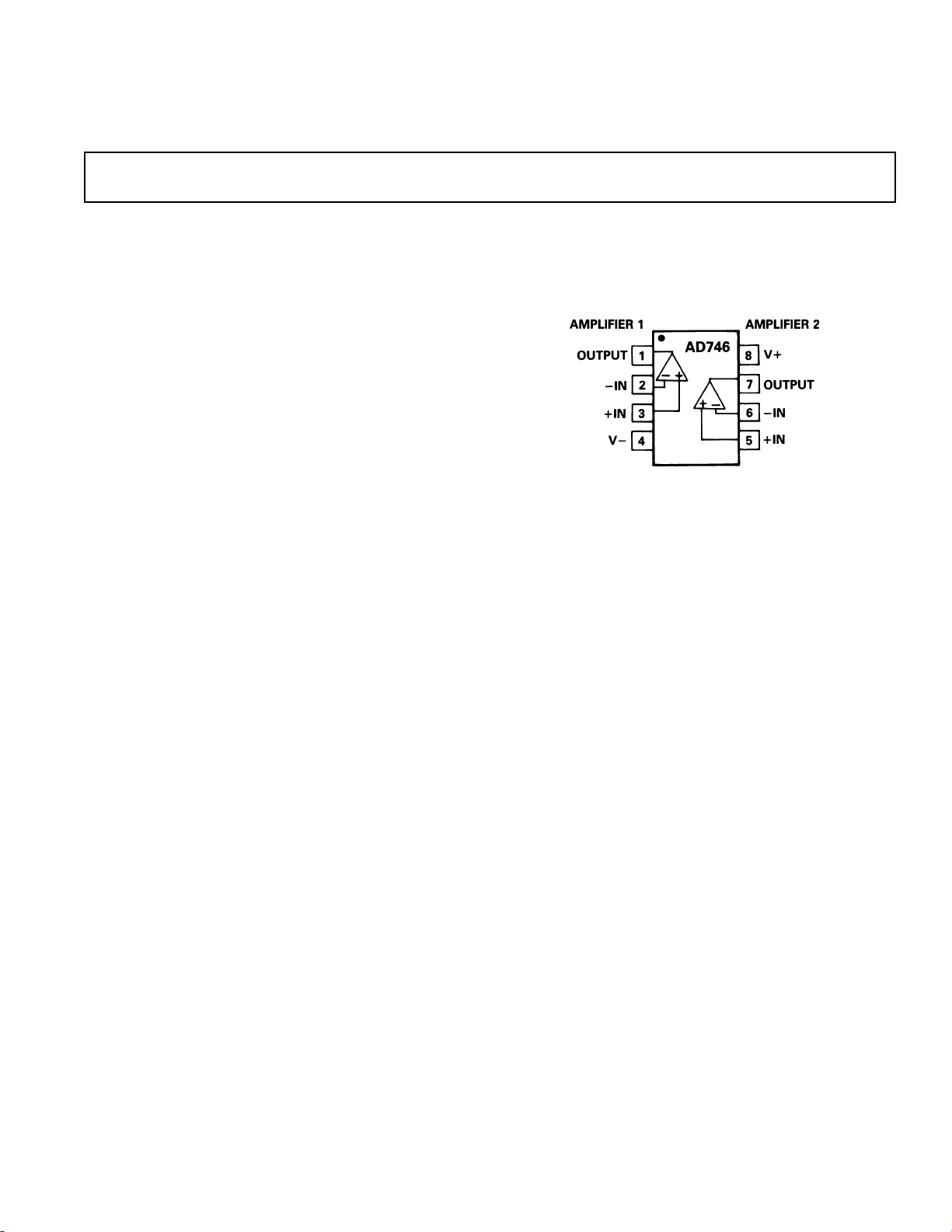
CONNECTION DIAGRAM
Plastic Mini-DIP (N)
Cerdip (Q) and
Plastic SOIC (R) Packages
The AD746 is available in three 8-pin packages: plastic mini
DIP, hermetic cerdip and surface mount (SOIC).
PRODUCT DESCRIPTION
The AD746 is a dual operational amplifier, consisting of two
AD744 BiFET op amps on a single chip. These precision
monolithic op amps offer excellent dc characteristics plus rapid
settling times, high slew rates and ample bandwidths. In
addition, the AD746 provides the close matching ac and dc
characteristics inherent to amplifiers sharing the same
monolithic die.
The single pole response of the AD746 provides fast settling:
500 ns to 0.01%. This feature, combined with its high dc
precision, makes it suitable for use as a buffer amplifier for 12or 14-bit DACs and ADCs. Furthermore, the AD746’s low total
harmonic distortion (THD) level of 0.0001% and very close
matching ac characteristics make it an ideal amplifier for many
demanding audio applications.
The AD746 is internally compensated for stable operation as a
unity gain inverter or as a noninverting amplifier with a gain of 2
or greater. It is available in four performance grades. The
AD746J is rated over the commercial temperature range of 0 to
+70°C. The AD746A and AD746B are rated over the industrial
temperature range of –40°C to +85°C. The AD746S is rated
over the military temperature range of –55°C to +125°C and is
available processed to MIL-STD-883B, Rev. C.
PRODUCT HIGHLIGHTS
1. The AD746 offers exceptional dynamic response for high
speed data acquisition systems. It settles to 0.01% in 500 ns
and has a 100% tested minimum slew rate of 50 V/µs
(AD746B).
2. Outstanding dc precision is provided by a combination of
Analog Devices’ advanced processing technology, laser wafer
drift trimming and well-matched ion-implanted JFETs. Input
offset voltage, input bias current and input offset current are
specified in the warmed-up condition and are 100% tested.
3. Differential and multichannel systems will benefit from the
AD746’s very close matching of ac characteristics. Input
offset voltage specs are fully tested and guaranteed to a
maximum of 0.5 mV (AD746B).
4. The AD746 has very close, guaranteed matching of input
bias current between its two amplifiers.
5. Unity gain stable version AD712 also available.
REV. B
Information furnished by Analog Devices is believed to be accurate and
reliable. However, no responsibility is assumed by Analog Devices for its
use, nor for any infringements of patents or other rights of third parties
which may result from its use. No license is granted by implication or
otherwise under any patent or patent rights of Analog Devices.
One Technology Way, P.O. Box 9106, Norwood, MA 02062-9106, U.S.A.
Tel: 617/329-4700 Fax: 617/326-8703
Page 2
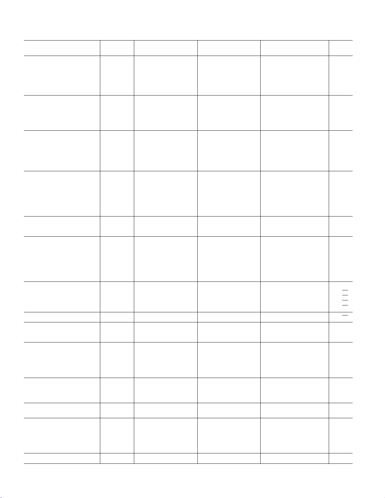
AD746–SPECIFICATIONS
(@ +258C and 615 V dc, unless otherwise noted)
Model Conditions Min Typ Max Min Typ Max Min Typ Max Units
AD746J/A AD746B AD746S
INPUT OFFSET VOLTAGE
1
Initial Offset 0.3 1.5 0.25 0.5 0.3 1.0 mV
Offset T
vs. Temperature 12 20 5 10 12 20 µV/°C
MIN
to T
MAX
2.0 0.7 1.5 mV
vs. Supply2 (PSRR) 80 95 84 100 80 95 dB
vs. Supply (PSRR) T
Long Term Stability 15 15 15 µV/month
INPUT BIAS CURRENT
Either Input VCM = 0 V 110 250 110 150 110 250 pA
Either Input @ T
Either Input VCM = +10 V 145 350 145 200 145 350 pA
Offset Current VCM = 0 V 45 125 45 75 45 125 pA
Offset Current @ T
MATCHING CHARACTERISTICS
Input Offset Voltage 0.6 1.5 0.3 0.5 0.6 1.0 mV
3
MAX
MAX
Input Offset Voltage T
Input Offset Voltage Drift 20 20 20 µV/°C
Input Bias Current 125 75 125 pA
MIN
to T
80 84 80 dB
MAX
VCM = 0 V 2.5/7 5.7/16 7 9.6 113 256 nA
VCM = 0 V 1.0/3 2.8/8 3 4.8 45 128 nA
MIN
to T
MAX
2.0 0.7 1.5 mV
Crosstalk @ 1 kHz 120 120 120 dB
@ 100 kHz 90 90 90 dB
FREQUENCY RESPONSE
Gain BW, Small Signal G = –1 8 13 9 13 8 13 MHz
Slew Rate, Unity Gain G = –1 45 75 50 75 45 75 V/µs
Full Power Response VO = 20 V p-p 600 600 600 kHz
Settling Time to 0.01%
Total Harmonic f = 1 kHz
Distortion R1 ≥ 2 kΩ
4
G = 1 0.5 0.75 0.5 0.75 0.5 0.75 µs
VO = 3 V rms 0.0001 0.0001 0.0001 %
INPUT IMPEDANCE
Differential 2.5 × l01li5.5 2.5 × l01li5.5 2.5 × l01li5.5 ΩipF
Common Mode 2.5 × l01li5.5 2.5 × l01li5.5 2.5 × l01li5.5 ΩipF
INPUT VOLTAGE RANGE
Differential
Common-Mode Voltage +14.5, –11.5 +14.5, –11.5 +14.5, –11.5 V
Over Max Operating Range
5
6
–11 +13 –11 +13 –11 +13 V
±20 ±20 ±20 V
Common-Mode Rejection Ratio VCM = ±10 V 78 88 82 88 78 88 dB
T
to T
MIN
VCM = ±11 V 72 84 78 84 72 84 dB
T
to T
MIN
INPUT VOLTAGE NOISE 0.1 to 10 Hz 2 2 2 µV p-p
f = 10 Hz 45 45 45 nV/ÏHz
76 84 80 84 76 84 dB
MAX
70 80 74 80 70 80 dB
MAX
f = 100 Hz 22 22 22 nV/ÏHz
f = 1 kHz 18 18 18 nV/ÏHz
f = 10 kHz 16 16 16 nV/ÏHz
INPUT CURRENT NOISE f = 1 kHz 0.01 0.01 0.01 pA/ÏHz
OPEN LOOP GAIN VO = ±10 V
R1 ≥ 2 kΩ 150 300 175 300 150 300 V/mV
T
MIN
to T
75 200 75 200 65 175 V/mV
MAX
OUTPUT CHARACTERISTICS
Voltage R1 ≥ 2 kΩ +13, –12.5 +13.9, –13.3 +13, –12.5 +13.9, –13.3 +13, –12.5 +13.9, –13.3 V
T
to T
Current Short Circuit 25 25 25 mA
MIN
±12 +13.8, –13.1 612 +13.8, –13.1 612 +13.8, –13.1 V
MAX
Max Capacitive Load Gain = –1 50 50 50 pF
Driving Capability Gain = –10 500 500 500 pF
POWER SUPPLY
Rated Performance ±15 ±15 ±15 V
Operating Range 64.5 618 64.5 618 64.5 618 V
Quiescent Current 7 10 7 8.0 7 10 mA
TEMPERATURE RANGE
Rated Performance 0 to +70/–40 to +85 –40 to +85 –55 to +125 °C
PACKAGE OPTIONS
8-Pin Plastic Mini-DIP (N-8) AD746JN
8-Pin Cerdip (Q-8) AD746AQ AD746BQ AD746SQ
8-Pin Surface Mount (R-8) AD746JR
Tape and Reel AD746JR-REEL
Chips AD746SCHIPS
TRANSISTOR COUNT 54 54 54
–2–
REV. B
Page 3
WARNING!
ESD SENSITIVE DEVICE
AD746
NOTES
1
Input Offset Voltage specifications are guaranteed after 5 minutes of operation at TA = +25°C.
2
PSRR test conditions: +VS = 15 V, –VS = –12 V to –18 V and +VS = 12 V to 18 V, –VS = –15 V.
3
Bias Current Specifications are guaranteed maximum at either input after 5 minutes of operation at T
10°C.
4
Gain = –1, Rl = 2 k, Cl = 10 pF.
5
Defined as voltage between inputs, such that neither exceeds ±10 V from ground.
6
Typically exceeding –14.1 V negative common-mode voltage on either input results in an output phase reversal.
Specifications subject to change without notice.
Specifications in boldface are tested on all production units at final electrical test. Results from those tests are used to calculate outgoing quality levels. All min and
max specifications are guaranteed, although only those shown in boldface are tested on all production units.
= +25°C. For higher temperature, the current doubles every
A
ABSOLUTE MAXIMUM RATINGS
Supply Voltage . . . . . . . . . . . . . . . . . . . . . . . . . . . . . . . . .±18 V
Internal Power Dissipation
2
. . . . . . . . . . . . . . . . . . . . . 500 mW
Input Voltage . . . . . . . . . . . . . . . . . . . . . . . . . . . . . . . . . . .±V
1
S
Output Short Circuit Duration
(For One Amplifier) . . . . . . . . . . . . . . . . . . . . . . . Indefinite
Differential Input Voltage . . . . . . . . . . . . . . . . . . +V
and –V
S
S
Storage Temperature Range (Q) . . . . . . . . . . –65°C to +150°C
Storage Temperature Range (N, R) . . . . . . . . –65°C to +125°C
Operating Temperature Range
AD746J . . . . . . . . . . . . . . . . . . . . . . . . . . . . . .0°C to +70°C
AD746A/B . . . . . . . . . . . . . . . . . . . . . . . . . .–40°C to +85°C
AD746S . . . . . . . . . . . . . . . . . . . . . . . . . . . –55°C to +125°C
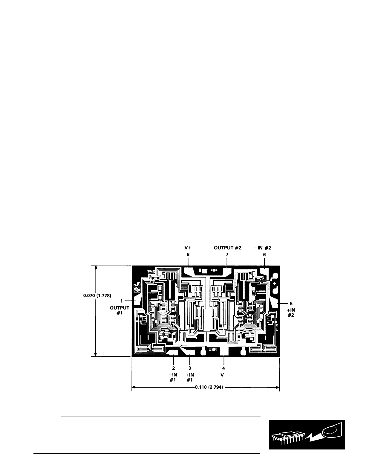
METALIZATION PHOTOGRAPH
Contact factory for latest dimensions.
Dimensions shown in inches and (mm).
Lead Temperature Range
(Soldering 60 seconds) . . . . . . . . . . . . . . . . . . . . . . . +300°C
ESD Rating . . . . . . . . . . . . . . . . . . . . . . . . . . . . . . . . . . . . . . .
NOTES
1
Stresses above those listed under “Absolute Maximum Ratings” may cause
permanent damage to the device. This is a stress rating only and functional
operation of the device at these or any other conditions above those indicated in
the operational section of this specification is not implied. Exposure to absolute
maximum rating conditions for extended periods may affect device reliability.
2
8-Pin Plastic Package: θJA = 100°C/Watt, θJC = 50°C/Watt
8-Pin Cerdip Package: θJA = 110°C/Watt, θJC = 30°C/Watt
8-Pin Small Outline Package: θJA = 160°C/Watt, θJC = 42°C/Watt
CAUTION
ESD (electrostatic discharge) sensitive device. Electrostatic charges as high as 4000 V readily
accumulate on the human body and test equipment and can discharge without detection.
Although the AD746 features proprietary ESD protection circuitry, permanent damage may
occur on devices subjected to high energy electrostatic discharges. Therefore, proper ESD
precautions are recommended to avoid performance degradation or loss of functionality.
REV. B
–3–
Page 4

AD746
–Typical Characteristics
Figure 1. Input Voltage Swing vs.
Supply Voltage
Figure 4. Quiescent Current vs.
Supply Voltage
Figure 2. Output Voltage Swing
vs. Supply Voltage
Figure 5. Input Bias Current vs.
Temperature
Figure 3. Output Voltage Swing
vs. Load Resistance
.
Figure 6. Output Impedance vs.
Frequency
Figure 7. Input Bias Current vs.
Common Mode Voltage
Figure 8. Short Circuit Current
Limit vs. Temperature
–4–
Figure 9. Gain Bandwidth Product
vs. Temperature
REV. B
Page 5

AD746
Figure 10. Open Loop Gain and
Phase Margin vs. Frequency
Figure 13. Common-Mode and
Power Supply Rejection vs.
Frequency
Figure 11. Settling Time vs.
Closed Loop Voltage Gain
Figure 14. Large Signal Frequency
Response
Figure 12. Open Loop Gain vs.
Supply Voltage
Figure 15. Output Swing and
Error vs. Settling Time
Figure 16. Total Harmonic
Distortion vs. Frequency Using
Circuit of Figure 19
REV. B
Figure 17. Input Noise Voltage
Spectral Density
–5–
Figure 18. Slew Rate vs. Input
Error Signal
Page 6

AD746
POWER SUPPLY BYPASSING
The power supply connections to the AD746 must maintain a
low impedance to ground over a bandwidth of 13 MHz or more.
This is especially important when driving a significant resistive
or capacitive load, since all current delivered to the load comes
from the power supplies. Multiple high quality bypass capacitors
are recommended for each power supply line in any critical
application. A 0.1 µF ceramic and a 1 µF tantalum capacitor as
shown in Figure 20 placed as close as possible to the amplifier
Figure 19. THD Test Circuit
(with short lead lengths to power supply common) will assure
adequate high frequency bypassing, in most applications. A
minimum bypass capacitance of 0.1 µF should be used for any
application.
If only one of the two amplifiers inside the AD746 is to be
utilized, the unused amplifier should be connected as shown in
Figure 21a. Note that the noninverting input should be
grounded and that R
and CL are not required.
L
Figure 20. Power Supply
Bypassing
Figure 21a. Gain of 2 Follower
Figure 22a. Unity Gain Inverter
Figure 21b. Gain of 2 Follower
Large Signal Pulse Response
Figure 22b. Unity Gain Inverter
Large Signal Pulse Response
–6–
Figure 21c. Gain of 2 Follower
Small Signal Pulse Response
Figure 22c. Unity Gain Inverter
Small Signal Pulse Response
REV. B
Page 7

AD746
A HIGH SPEED 3 OR AMP INSTRUMENTATION AMPLIFIER CIRCUIT
The instrumentation amplifier circuit shown in Figure 23 can
provide a range of gains from 2 up to 1000 and higher. The
circuit bandwidth is 2.5 MHz at a gain of 2 and 750 kHz at a
gain of 10; settling time for the entire circuit is less than 2 µs to
within 0.01% for a 10 volt step, (G = 10).
Figure 23. A High Performance, 3 Op Amp, Instrumentation Amplifier Circuit
Table I. Performance Summary for the 3 Op Amp
Instrumentation Amplifier Circuit
T
Gain R
G
Bandwidth (0.01%)
SETTLE
2 20 kΩ 2.5 MHz 1.0 µs
10 4.04 kΩ 1 MHz 2.0 µs
100 404 Ω 290 kHz 5.0 µs
Figure 25. Settling Time of the 3 Op
Amp Instrumentation Amplifier.
µ
Gain = 10, Horizontal Scale: 0.5
Vertical Scale: 5 V/Div.
Error Signal Scale: 0.01%/Div.
THD Performance Considerations
s/Div,
The AD746 was carefully optimized to offer excellent
performance in terms of total harmonic distortion (THD) in
signal processing applications. The THD level when operating
the AD746 in inverting gain applications will show a gradual
rise from the distortion floor of 20 dB/decade (see Figure 28).
In noninverting applications, care should be taken to balance
the source impedances at both the inverting and noninverting
inputs, to avoid distortion caused by the modulation of input
capacitance inherent in all BiFET op amps.
REV. B
Figure 24. Pulse Response of the 3
Op Amp Instrumentation Amplifier.
Gain = 10, Horizontal Scale:
µ
s/Div, Vertical Scale: 5 V/Div.
0.5
Figure 26. THD Measurement, Inverter Circuit
Figure 27. THD Measurement, Follower Circuit
–7–
Page 8

AD746
Figure 28. THD vs. Frequency Using Standard Distortion
Analyzer
2kΩ
SINE WAVE
GENERATOR
20V p-p
OUTPUT
LEVEL
2kΩ
–
2
1/2
AD746
+
3
4
–V
S
1µF 0.1µF
1
+
V
OUT
#1
20V p-p
OUTLINE DIMENSIONS
Dimensions shown in inches and (mm).
Mini-DIP (N) Package
C1319–10–9/89
Cerdip (Q) Package
20kΩ
+V
2.21kΩ
–
6
8
1/2
AD746
+
5
CROSSTALK = 20 LOG
S
+
1µF 0.1µF
7
10
Figure 29. Crosstalk Test Circuit
Figure 30. Crosstalk vs. Frequency
V
OUT
#2
V
#1
OUT
+ 20dB
V
#2
OUT
Plastic Small Outline
(R) Package
PRINTED IN U.S.A.
–8–
REV. B
 Loading...