

Page 1
Low Cost, Low Power
=
Preliminary Technical Data
FEATURES
2.5V Stereo Audio Codec with 3.3 V Tolerant Digital
Interface
Supports 96 kHz Sample Rates
Supports 16/18 /20/24-Bit Word Lengths
Multibit Sigma Delta Modulators with
“Perfect Differential Linearity Restoration” for
Reduced Idle Tones and Noise Floor
Data Directed Scrambling DACs - Least Sensitive to Jitter
Performance (20 Hz to 20 kHz)
90 dB ADC and DAC SNR
Digitally Programmable Input/Output Gain
On-chip Volume Controls Per Output Channel
Hardware and Software Controllable Clickless Mute
Supports 256xFs, 512xF
Master Clock Pre-Scaler for use with DSP master clocks
Flexible Serial Data Port with Right-Justified, LeftJustified, I
2
S-Compatible and DSP Serial Port Modes
Supports Packed Data Mode (“TDM”) for cascading
devices.
On-Chip Reference
16, 20 and 24-Lead SOIC, SSOP and TSSOP Package
options.
APPLICATIONS
Digital Video Camcorders (DVC)
Portable Audio Devices (Walkman etc)
Audio Processing
Voice Processing
Conference Phones
General Purpose Analog I/O
and 768xFs Master Mode Clocks
s
PRELIMINARY
TECHNICAL
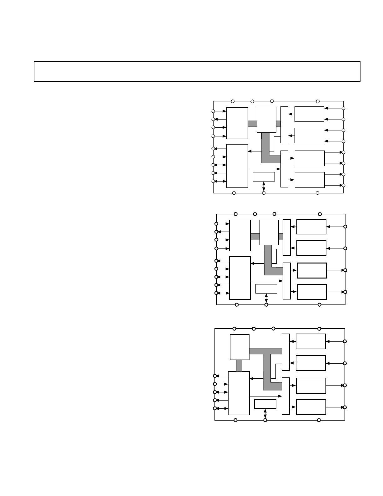
Stereo Audio Analog Front End
DVDD1(EXT)
CDIN
CDOUT
CCLK
CLATCH
ASDATA/SDO
DSDATA/SDI
LRCLK/SDIFS
SDOFS
BCLK/SCLK
CDIN
CDOUT
CCLK
CLATCH
ASDATA
DATA
DSDATA
LRCLK
BCLK
SPI
Port
I2S
Port
DGND
DVDD1(EXT)
SPI
Port
I2S
Port
AD74322
FUNCTIONAL BLOCK DIAGRAM
CLKINDVDD2(INT)
Control
Block
Reference
CLKINDVDD2(INT)
Control
Block
Reference
AVDD
ADC
CHANNEL 1
ADC
CHANNEL 2
DAC
CHANNEL 1
DAC
CHANNEL 2
AGNDREFCAP
AVDD
ADC
CHANNEL 1
ADC
CHANNEL 2
DAC
CHANNEL 1
DAC
CHANNEL 2
VIN1P
VIN1N
VIN2P
VIN2N
VOUT1P
VOUT1N
VOUT2P
VOUT2N
VIN1
VIN2
VOUT1
VOUT2
GENERAL DESCRIPTION
The AD74322 is a front-end processor for general purpose
audio and voice applications. It features two multi-bit Σ∆
A/D conversion channels and two multi-bit Σ∆ D/A
conversion channels. Each ADC channel provides >85 dB
signal-to-noise ratio while each DAC channel provides
>90 dB, both over an audio signal bandwidth.
The AD74322 is particularly suitable for a variety of applications where stereo input and output channels are
required, including audio sections of Digital Video
Camcorder, portable personal audio devices and the
analog front ends of conference phones . Its high quality
performance also make it suitable for speech and telephony
applications such as speech recognition and synthesis and
modern feature phones.
REV. Pr D 03/00
Information furnished by Analog Devices is believed to be accurate and
reliable. However, no responsibility is assumed by Analog Devices for its
use, nor for any infringements of patents or other rights of third parties
which may result from its use. No license is granted by implication or
otherwise under any patent or patent rights of Analog Devices.
DGND
DVDD1(EXT)
Control
Block
SDO
SDI
SDIFS
SDOFS
SCLK
One T echnolog y Way, P .O . Box 91 06, Norwood, MA 02062-9106, U.S.A.
T e l: 781/329-4700 World Wide W eb Site: http://www .analog.com
Fax: 781/326-8703 Analog Devices, Inc., 1998
Data
Port
DGND
CLKINDVDD2(INT)
Reference
AGNDREFCAP
AVDD
ADC
CHANNEL 1
ADC
CHANNEL 2
DAC
CHANNEL 1
DAC
CHANNEL 2
AGNDREFCAP
VIN1
VIN2
VOUT1
VOUT2
Page 2

AD74322
An on-chip reference voltage is included but can be
bypassed if required for use with an external reference
source.
The AD74322 offers sampling rates which, depending on
MCLK selection and MCLK divider ratio, range from 8
kHz in the voiceband range to 96 kHz in the audio range.
The digital interface to the AD74322 is configured as two
separate ports which allow separation of device control
and data streams. Control and status are monitored using
®
an SPI
data streams are controlled using an I
2
I
Left/Right Clock pins. There is also a DSP mode
available on the audio data port which will also allow both
control and data to be streamed through the same interface
where controller resources are limited.
The AD74322 is available in various lead count package
options. These range from a 16-pin variant with singleended inputs/outputs and no SPI port through a 20-pin
variant with single-ended inputs/outputs and an SPI port
to a 24-pin variant with differential inputs/outputs and an
SPI port. These devices will be available in SOIC, SSOP
and TSSOP package options and are specified for the
industrial temperature range of -40°C to +85°C.
compatible serial port while the input and output
S streams are controlled by a common Bit-Clock and
2S®
port. The two
PRELIMINARY TECHNICAL DA TA
PRELIMINARY
TECHNICAL
DATA
– 2 – Pr D 03/00
Page 3

PRELIMINARY TECHNICAL DA TA
AD74322A
PARAMETER Min Ty p Max Units Test Conditions
ANALOG-TO-DIGITAL CONVERTERS
ADC Resolution (all ADCs) 24 Bits
Dynamic Range (20 Hz to 20 kHz, -60 dB Input)
No Filter 9 0 d B
With A-Weighted Filter 9 2 d B
Total Harmonic Distortion + Noise -85(0.0056) dB(%)
Interchannel Isolation TBD d B
Interchannel Gain Mismatch TBD d B
Programmable Input Gain 12 dB
Gain Step Size 3 d B
Offset Error 0 LSB
Full Scale Input Voltage At Each Pin 0.5 (1.414) Vrms (Vpp) Single Ended
Automatic Level Control
Attack Time Resolution TBD Bits
Attack Time T BD µs/Bit
Decay Time Resolution TBD Bits
Decay Time TB D µs/Bit
Gain Drift TBD ppm/°C
Input Resistance 10 kΩ
Input Capacitance 15 p F
Common Mode Input Volts 1.1V V
DIGITAL-TO-ANALOG CONVERTERS
Dynamic Range (20 Hz to 20 kHz, -60 dB Input)
No Filter 9 0 d B
With A-Weighted Filter 9 2 d B
Total Harmonic Distortion + Noise -85(0.0056) dB(%)
Interchannel Isolation TBD d B
Interchannel Gain Mismatch TBD dB(%)
DC Accuracy
Gain Error T B D %
Interchannel Gain Mismatch TBD ppm/°C
Gain Drift T BD d B
Interchannel Crosstalk (EIAJ method) TBD d B
Interchannel Phase Deviation TBD Degrees
Volume Control Step Size (1023 Linear Steps) 0.098 %
Volume Control Range (Max Attenuation) 60 dB
Mute Attenuation -100 d B
De-emphasis Gain Error +/- 0.1 d B
Full Scale Output Voltage At Each Pin 0.5 (1.414) Vrms(Vpp) Single Ended
Output Resistance At Each Pin ?? ?? Ω
Common Mode Output Volts 2.25 V
REFERENCE (Internal)
Absolute Voltage, V
V
TC T BD ppm/°C
REF
ADC DECIMATION FILTER
Pass Band 0.xxxFs Hz
Pass Band Ripple ±0.00xx d B
Transition Band 0.xxFs 0.xxFs Hz
Stop Band 0.xxFs H z
Stop Band Attenuation 7 0 d B
Group Delay lll/Fs nnn/Fs mmm/Fs m s
DAC INTERPOLATION FILTER
Pass Band 0.xxxFs Hz
Pass Band Ripple ±0.00xx d B
Transition Band 0.xxFs 0.xxFs Hz
Stop Band 0.xxFs H z
Stop Band Attenuation 7 0 d B
Group Delay lll/Fs nnn/Fs mmm/Fs m s
PR D 03/00
REF
PRELIMINARY
TECHNICAL
DATA
1.1 V
–3–
AD74322
Page 4
AD74322–SPECIFICA TIONS
PARAMETER Min Typ Max Units Test Conditions
LOGIC INPUT
V
, Input High Voltage DVDD1 - 0.8 DVDD1 V
INH
, Input Low Voltage 0 0. 8 V
V
INL
Input Current -10 +10 µA
Input Capacitance 10 p F
LOGIC OUTPUT
VOH, Output High Voltage DVDD1 - 0.4 DVDD1 V
, Output Low Voltage 0 0.4 V
V
OL
Three-State Leakage Current -10 +10 µA
POWER SUPPLIES
AVDD, DVDD2 2.25 2.5 2.75 V
DVDD1 2.7 3.0 3.3 V
POWER CONSUMPTION
All Sections On TBD m A
ADCs On Only TB D mA
DACs On Only TB D mA
Reference On Only TBD m A
Powerdown Mode TBD µA
(AVDD = DVDD2 = +2.5V ±10%, DVDD1 = 3.0V ±10%, f
f
= 48 kHz, TA = T
SAMP
AD74322A
MIN
to T
, unless otherwise noted)
MAX
CLKIN
= 12.288 MHz,
PRELIMINARY
TECHNICAL
DATA
–4–
Pr D 03/00
Page 5
PRELIMINARY TECHNICAL DA TA
ORDERING GUIDE
Model Range Package
AD74322DAR -40 C to +85 C R-16
AD74322DARU -40 C to +85 C RU-16
AD74322AAR -40 C to +85 C R-20
AD74322AARU -40 C to +85 C RU-20
AD74322AAR -40 C to +85 C R-24
AD74322AARU -40 C to +85 C RU-24
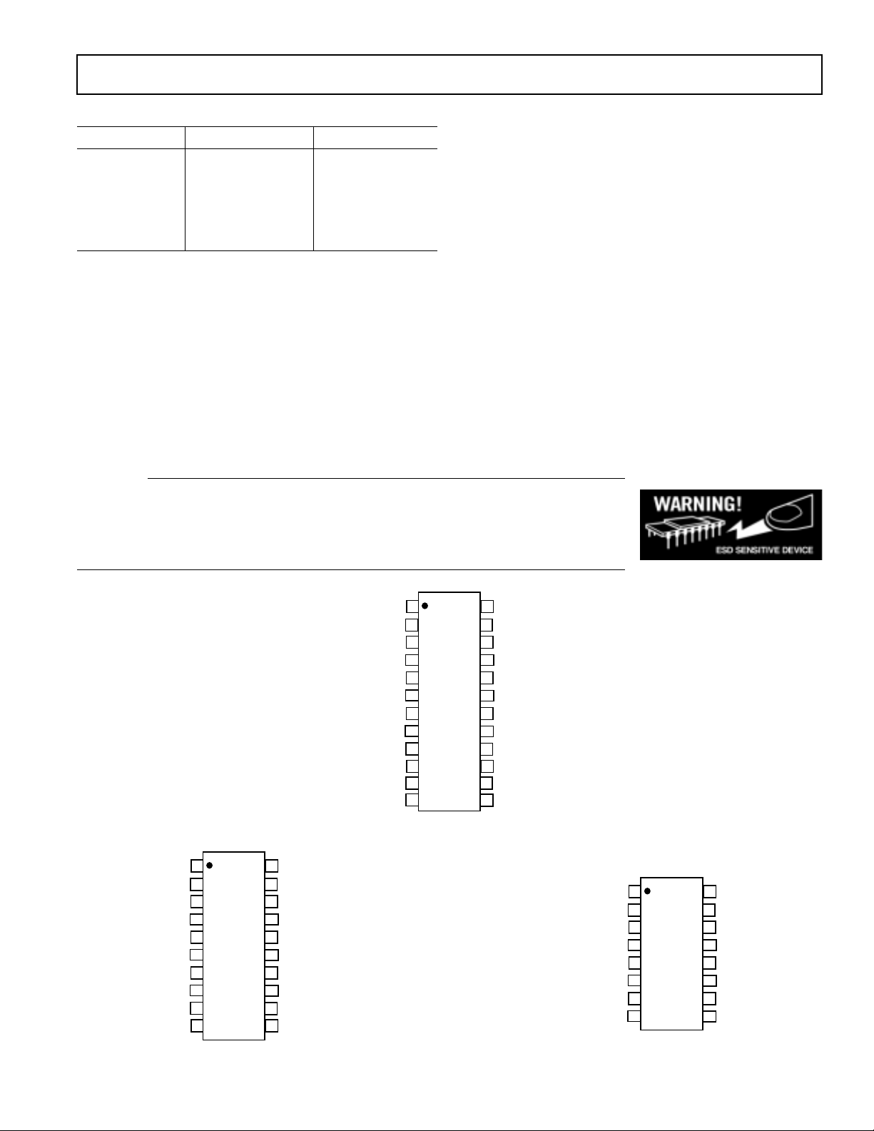
CAUTION
ESD (electrostatic discharge) sensitive device. Electrostatic charges as high as 4000 V readily
accumulate on the human body and test equipment and can discharge without detection.
Although the XX0000 features proprietary ESD protection circuitr y, permanent damage may
occur on devices subjected to high energy electrostatic discharges. Therefore, proper ESD
precautions are recommended to avoid performance degradation or loss of functionality.
PRELIMINARY
AD74322
VOUTP2VINP2
1
VINP1
VINP1
2
3
AGND
4
DGND
5
DVDD2
6
CIN
TOP VIEW
7
(Not to Scale)
8
9
10
DVDD1
MCLK SCLK
CCLK
20
19
18
17
16
15
14
13
12
11
VOUTP1
VOUTP1
AVDDREFCAP
RESET
SDO
SDFS
SDI
COUT
CLATCH
TECHNICAL
VINN1
1
VINN2
VINP1
AGND
DGND
DVDD2
DVDD1
MCLK SCLK
CCLK
CIN
DATA
2
3
4
5
6
7
8
TOP VIEW
9
(Not to Scale)
10
11
12
24
23
22
21
20
19
18
17
16
15
14
13
VOUTN1
VOUTN2
VOUTN1VINN1
VOUTP1
AVDDREFCAP
RESET
SDO
SDFS
SDI
COUT
CLATCH
1
VINP1
VINP1
2
3
AGND
4
DGND
5
DVDD2
6
DVDD1
7
MCLK SCLK
8
TOP VIEW
(Not to Scale)
16
15
14
13
12
11
10
9
VOUTP2VINP2
VOUTP1
VOUTP1
AVDDREFCAP
RESET
SDO
SDFS
SDI
–5–Pr D 03/00
Page 6

AD74322
PIN FUNCTION DESCRIPTION (SINGLE-ENDED I/O ; NO SPI PORT)
Mnemonic I/O Function
VIN1 I Analog Input - Channel 1
VIN2 I Analog Input - Channel 2
VOUT1 O Analog Output - Channel 1
VOUT2 O Analog Output - Channel 2
REFCAP I/O Internal Reference - Can also be used for connection of an external reference
AVDD Analog Power Supply Connection
AGND Analog Ground/Substrate Connection
DVDD1 Digital Power Supply Connection (Interface)
DVDD2 Digital Power Supply Connection (Core)
DGND Digital Ground/Substrate Connection
MCLK I External Clock Connection
SDO O ADC Serial Data Out - DSP Mode
SDI I DAC Serial Data In - DSP Mode
SDFS I/O Serial Data Input Frame Sync - DSP Mode
4-5-6 I Powerdown/Reset Input
SCLK I/O Serial Clock - DSP Mode
PIN FUNCTION DESCRIPTION (SINGLE-ENDED I/O WITH SPI PORT)
Mnemonic I/O Function
VIN1 I Analog Input - Channel 1
VIN2 I Analog Input - Channel 2
VOUT1 O Analog Output - Channel 1
VOUT2 O Analog Output - Channel 2
REFCAP I/O Internal Reference - Can also be used for connection of an external reference
AVDD Analog Power Supply Connection
AGND Analog Ground/Substrate Connection
DVDD1 Digital Power Supply Connection (Interface)
DVDD2 Digital Power Supply Connection (Core)
DGND Digital Ground/Substrate Connection
MCLK I External Clock Connection
CDIN I Serial Data In on SPI Control Port
CDOUT O Serial Data Out on SPI Control Port
CCLK I Serial Clock on SPI Control Port
CLATCH I Serial Data Latch on SPI Control Port
ASDATA O ADC Serial Data Out - I
DSDATA I DAC Serial Data In - I
LRCLK/ I/O Left/Right Channel Select - I
BCLK I/O Bit Clock - I
RESET I Powerdown/Reset Input
PRELIMINARY
TECHNICAL
DATA
2
S
2
S
2
S
2
S
PRELIMINARY TECHNICAL DA TA
– 6 – Pr D 03/00
Page 7

PRELIMINARY TECHNICAL DA TA
PIN FUNCTION DESCRIPTION (DIFFERENTIAL I/O WITH SPI PORT)
Mnemonic I/O Function
VINP1 I Analog Input - Channel 1 Positive
VINN1 I Analog Input - Channel 1 Negative
VINP2 I Analog Input - Channel 2 Positive
VINN2 I Analog Input - Channel 2 Negative
VOUTP1 O Analog Output - Channel 1 Positive
VOUTN1 O Analog Output - Channel 1 Negative
VOUTP2 O Analog Output - Channel 2 Positive
VOUTN2 O Analog Output - Channel 2 Negative
REFCAP I/O Internal Reference - Can also be used for connection of an external reference
AVDD Analog Power Supply Connection
AGND Analog Ground/Substrate Connection
DVDD1 Digital Power Supply Connection (Interface)
DVDD2 Digital Power Supply Connection (Core)
DGND Digital Ground/Substrate Connection
MCLK I External Clock Connection
CDIN I Serial Data In on SPI Control Port
CDOUT O Serial Data Out on SPI Control Port
CCLK I Serial Clock on SPI Control Port
CLATCH I Serial Data Latch on SPI Control Port
ASDATA O ADC Serial Data Out - I
DSDATA I DAC Serial Data In - I
LRCLK/ I/O Left/Right Channel Select - I
BCLK I/O Bit Clock - I
RESET I Powerdown/Reset Input
2
S
2
S
2
S
2
S
AD74322
PRELIMINARY
TECHNICAL
DATA
–7–Pr D 03/00
Page 8

AD74322
PRELIMINARY TECHNICAL DA TA
FUNCTIONAL DESCRIPTION
ADC Section
There are two ADC channels in the AD74322, configured as a stereo
pair. Each ADC channel can be independently muted. The input pins
are switched between differential inputs or four single ended inputs
accordingly. The gain block can be programmed for independent left and
right gains, in steps of +3dB, from 0dB to +12dB. The ADC operates at
an oversampling ratio of 128 and the decimation filter reduces the output
to the standard sample rates. The output maximum
sample rate is 96 kHz at ASDATA.
Automatic Level Control
Analog Sigma Delta Modulator
Decimator Section
The digital decimation filter has a passband ripple of ±0.01dB and a
stopband attenuation of 70dB. The filter is an FIR type with a linear
phase response. The group delay at 48kHz is ??us. Output sample rates
up to 96 kHz are supported.
Input Signal swing
Each ADC input has an input range of 0.5 V
Ended) about a bias point equal to V
REFCAP
/ 1.414 V
RMS
(See Figure
(Single-
P-P
<Input_Swing>)
AD743xx
V
P-P
P-P
REFCAP
V
REFCAP
VINPx
PRELIMINARY
VINNx
1.414 V
1.414 V
TECHNICAL
Figure <Input_Swing>
DAC Section
The AD74322 has two DAC channels arranged as a stereo pair, with two,
fully differential voltage, analog outputs for improved noise and distortion
performance. Each channel has it’s own independently programmable
attenuator with a maximum attenuation of 63dB, adjustable in 1dB steps.
Digital inputs are via a serial data input pin and a common frame
(DLRCLK) and bit (DBLCK) clock or using a ‘packed data’ mode, both
channels can be input using a single data pin.
Interpolator Section
Digital Sigma Delta Modulator
DAC
Analog Output Filter
Output Signal swing
Each ADC input has an output range of 0.5 V
Ended) about a bias point equal to V
REFCAP
<Output_Swing>)
/ 1.414 V
RMS
(See Figure
(Single-
P-P
Reference
The AD74322 features an on-chip reference whose
nominal value is 1.125 V.A __ nF capacitor applied at the
REFCAP pin is necessary to stabilise the referrence. (See
Figure <REFCAP_Int>)
AD743xx
REFCAP
Figure <REFCAP_Int>
If it is required to use an external reference, because of its value or its
reference tempco, the internal reference can be disabled via Control
Register __ and the external reference applied at the REFCAP pin (See
Figure <REFCAP_Ext>).
AD743xx
1.0 V
EXTERNAL
REFERENCE
REFCAP
DATA
Figure <REFCAP_Ext>
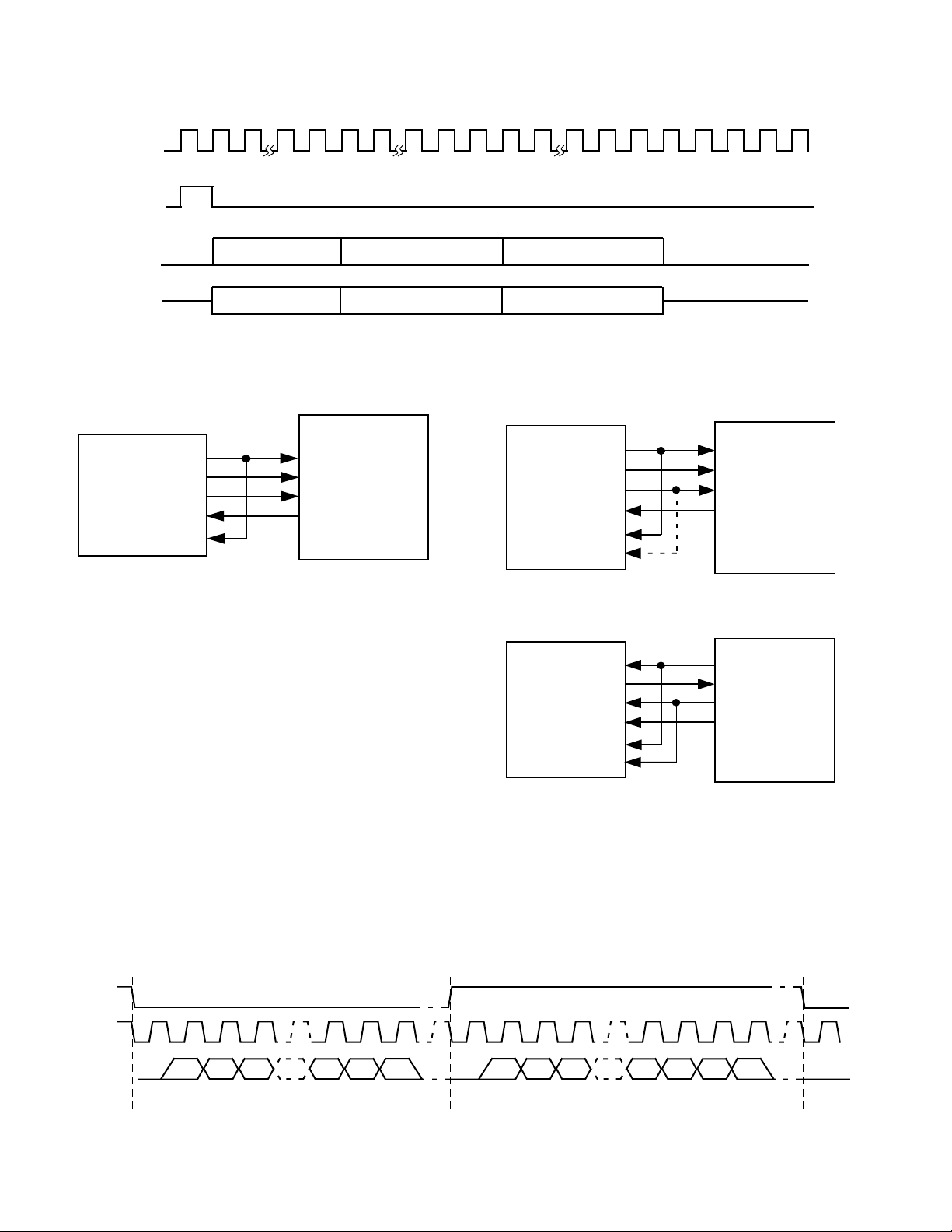
Master Clocking Scheme
The update rate of the AD74322’s ADC and DAC channels require an
internal master clock (IMCLK) which is 256 times that sample update
rate (IMCLK = 256 * F
selecting sample rates, the device has a series of three
master clock pre-scalers which are programmable and
allow the user to choose a range of convenient sample
rates from a single external master clock. The master
clock signal to the AD74322 is applied at the MCLK pin.
The MCLK signal is passed through a series of two
programmable MCLK pre-scalers (divider) circuits which
can be selected to reduce the resulting Internal MCLK
(IMCLK) frequency if required. The first MCLK prescaler provides divider ratios of /1 (pass through), /2, /3
while the second pre-scaler provides divider ratios of ./1
(pass through), /2, /4 and the third pre-scaler provides
ratios of /1 (pass through), /2 and /5..
). In order to provide some flexibility in
S
1.414 V
1.414 V
P-P
P-P
V
REFCAP
V
REFCAP
Figure <Output_Swing>
AD743xx
VOUTPx
VOUTNx
Programmable
MCLK
/1
/2
/3
Divider
Control Reg
/1
/2
/4
Pre-Scaler 1 Pre-Scaler 2
MCLK IMCLK
– 8 – Pr D 03/00
Page 9

PRELIMINARY TECHNICAL DA TA
AD74322
FILTER
AVDD VDD2 VDD1
2.4 V
3.3 V
REGULATOR
4
AD743xx
4
AGND DGND
Figure <PSU_Connection>
Figure <MCLK_Divider>
The divider ratios will allow more convenient sample rate
selection from a common MCLK which may be required
in many voice related applications.
Example 1: f
MCLK = 48*103 * 256 = 12.288 MHz to cater for 48
kHz f
SAMP
For f
Pre-Scaler 1, the /2 setting in Pre-Scaler 2 and pass
through in Pre-Scaler 3. This results in an IMCLK =
8*10
Example 2: f
MCLK = 24.576 MHz
For f
Pre-Scaler 1 and the /1 (pass-through) setting in PreScaler 2 and pass through in Pre-Scaler 3. This results in
an IMCLK = 48*10
For f
Pre-Scaler 1 and the /1 (pass-through) setting in PreScaler 2 and pass through in Pre-Scaler 3. This results in
an IMCLK = 32*10
Example 3: fSAMP = 44.1 kHz and 11.025 kHz required
MCLK = 44.1*103 * 256 = 11.2896 MHz to cater for
44.1 kHz f
For f
Scaler 1 and the /4 setting in Pre-Scaler 2 and pass
through in Pre-Scaler 3. This results in an IMCLK =
11.025*10
Sample Rates
For all applications the sampling rate is defined by the internal master
clock frequency (IMCLK) where IMCLK = 256 * f
Power-On Reset
The AD74322 features a power-on reset circuit which
ensures that all internal circuitry is reset and initialised to
= 8 kHz, it is necessary to use the /3 setting in
SAMP
3
* 256 = 2.048 MHz (= 12.288 MHz/6).
= 48 kHz, it is necessary to use the /2 setting in
SAMP
= 32 kHz, it is necessary to use the /3 setting in
SAMP
= 11.025 kHz, it is necessary to use the /1 setting in Pre-
SAMP
= 48 kHz and 8 kHz required
SAMP
= 48 kHz and 32 kHz required
SAMP
3
* 256 = 12.288 MHz.
3
* 256 = 8.192 MHz.
SAMP
3
* 256 = 2.8224 MHz (= 11.2896 MHz/4).
PRELIMINARY
TECHNICAL
DATA
.
SAMP
–9–Pr D 03/00
DUAL
5.0 V
DVDD
DSP
DGND
a known state following the power-up of the device. There
is also a software reset capability available by setting the
RESET bit in Control Register _. This control register is
accessed through the Control Port.
Power Supplies and Grounds
The AD74322 features three separate supplies: AVDD,
DVDD1 and DVDD2.
AVDD is the supply to the analog section of the device
and must therefore be of sufficient quality to preserve the
AD74322’s performance characteristics. It is nominally a
2.4 V supply.
DVDD1 is the supply for the digital interface section of
the device. It is fed from the digital supply voltage of the
DSP or controller to which the device is interfaced and
allows the AD74322 to interface with devices operating at
supplies of between 2.4 V -5% to 3.3 V + 10%.
DVDD2 is the supply for the digital core of the
AD74322. It is nominally a 2.4 V supply.
Page 10

AD74322
KLCM
)zHM(
840.2 84-2--1----
882.218442-21--6----
483.614623-61--8----
675.426984-42--21----
468.63--84--42---21-
PRELIMINARY TECHNICAL DA TA
)sf652semussa(soitaR)rediviD(ralacSgnisu)zHk(setaRgnilpmaS
12345689 012151
Table <MCLK_Divider>
PRELIMINARY
etaRgnilpmaS
f
S
)zHk(
8
61
1.11
2.22
23
46
1.44
2.88
84
69
rotalopretnI
edoM
)lamroN(x8
)elbuoD(x4
)lamroN(x8
)elbuoD(x4
)lamroN(x8
)elbuoD(x4
)lamroN(x8
)elbuoD(x4
)lamroN(x8
)elbuoD(x4
DATA
f652
S
840.2690.4441.6
4228.28446.52764.8
291.8483.61675.42
6982.112975.228868.33
882.21675.42468.63
f215
TECHNICAL
)zHM(KLCM
S
f867
S
Table <MCLK_Select>
–10– Pr D 03/00
Page 11

PRELIMINARY TECHNICAL DA TA
LRCLK/SDIFS
SDOFS
DSDATA/SDI
BCLK/SCLK
ASDATA/SDO
AD743xx
(MASTER)
TFS
DT
SCLK
DR
RFS
DSP
(SLAVE)
AD74322
INTERFACING
The AD74322 features two separate interfaces, Control and Data, which
are used to program control settings and send/receive sample data
respectively. The Control interface is implemented using an SPI type
protocol but transfers 16-bits per frame. The Data interface uses either a
DSP or I
and codec. The DSP compatible interface mode allows data samples to be
transferred in a protocol that is supported by the serial interfaces of most
fixed- and floating-point DSPs.
In order to reduce peripheral requirements when interfacing the AD74322
with the host DSP, the DSP mode allows the DSP to send both data and
control information to the device via the data interface. This is the default
mode and requires users to only use a single DSP SPORT to both control
the device and service it with data samples.
Control Interface
Control of the AD74322 operation is via a set of 16 Control Registers
which are programmed through the Control Port. The Control Port
protocol is similar to the SPIÒ protocol with the exception that 16-bits of
data are transferred per frame. The Control Port consists of the following
pins: CCLK - Control Port Serial Clock, CLATCH - Control Port Latch
or Frame signal, CDIN - Control Port Serial Data In and CDOUT Control Port Data Out. CLATCH is a framing signal that is active low.
When asserted, it gates the other interface lines as being active. CCLK is
used to clock input data on CDIN and clock output (readback) data on
CDOUT. Figure <Control_Interface> details the connectivity of the
Control Port to a controller and Figure <Control_Timing> details the
interface timing.
2
S protocol to transfer stereo data samples between controller
PRELIMINARY
AD743xx
TECHNICAL
CDIN CLATCH CCLK CDOUT
DATA
Data in and out of the Control Port go through a 16-bit
shift register whose contents are mapped to the internal
registers using the mapping scheme of Figure
<ContPortMap>. A 16-bit word received by the Control
Port is decoded as a read or write to a register address set
by bits 15 - 12. This 4-bit register address selects 1 of 16
registers as shown in Table <ContRegMap>. Bit 11
selects whether a register read or write is requested Write = 0, Read = 1. Bit-10 is reserved. Bits 9 through 0
contain register data. Each Control register’s contents are
detailed below.
Data Interface
There are two modes of operation of the data interface: DSP mode and
I2S mode. The default mode of the data interface is a DSP mode which
combines control and data functions in a single protocol. This is to reduce
the peripheral overhead required on the DSP when interfacing to the
AD74322. This mode operates in a standard DSP serial format. In I2S
mode the data interface streams audio data samples being sent to or
received from the DACs and ADCs respectively, using the I2S serial
protocol.
In either mode it can be configured as either a master or slave device
ensuring connectivity to the largest number of host processors.
DSP Mode
The DSP mode allows interfacing to most fixed- and floating-point DSPs
as well as other processors such as RISCs etc that having serial ports that
support synchronous communications. The key feature of synchronous
DSP communications is that the serial data is framed by a separate Frame
Sync signal. Figures <Data_DSP_Slave> and <Data_DSP_Master> detail
connectivity in Master Mode (codec is master) and Slave Mode (codec is
slave) respectively.
CONTROLLER
Figure <Control_Interface>
CCLK
CDIN
CDOUT
CLATCH
MSB 14 13 12 11 10 9 8 7 6 5 4 3 2 1 LSB
MSB 14 13 12 11 10 9 8 7 6 5 4 3 2 1 LSB
Figure <Data_DSP_Slave>
Figure <Control_Timing>
–11–Pr D 03/00
Page 12
AD74322
BCLK/
SCLK
LRCLK/
FS
PRELIMINARY TECHNICAL DA TA
DSDATA/
SDI
ASDATA/
SDO
CONTROL LEFT DAC RIGHT DAC
STATUS LEFT ADC RIGHT ADC
Figure <DSP_Protocol>
AD743xx
(SLAVE)
LRCLK/SDIFS
DSDATA/SDI
BCLK/SCLK
ASDATA/SDO
SDOFS
DSP
(MASTER)
TFS
DT
SCLK
DR
RFS
Figure <Data_DSP_Master>
The serial protocol uses a fixed position for data being sent to or received
PRELIMINARY
from the Left and Right DACs and ADCs respectively and the control
words being sent to and the status words being received from the device
respectively. Figure <DSP_Protocol> details the arrangement of both
TECHNICAL
audio and control/status information in the serial transfer.
I2S
(Inter IC Sound Bus) Mode
The I2S bus is a three line serial bus which features a serial data line
carrying both left and right (stereo) channels. The Left and Right channel
information are selected by the status of the Left/Right Clock (Word
Select) line. Serial data is clocked by the Bit Clock line. Figures
<Data_I2S_DSP_Master> and <Data_I2S_DSP_Slave> detail the
interface configuration between controller and codec in I
controller as master and slave respectively. Figure <> details I
2
S mode with
2
S timing.
The interface allows easy transfer of arbitrary length serial data samples
sent MSB first. Toggling of the Left/Right Clock line indicates that the
end of the current word will occur after the following Bit Clock cycle and
the start of the alternate channel word will occur on the subsequent Bit
Clock cycle
TFS
ADSP-
21065L
(MASTER)
TCLK
DR
RFS
RCLK
Figure <Data_I2S_DSP_Master>
DATA
ADSP-
21065L
(MASTER)
TFS
TCLK
DR
RFS
RCLK
Figure <Data_I2S_DSP_Slave>
DT
DT
LRCLK/SDIFS
DSDATA/SDI
BCLK/SCLK
ASDATA/SDO
AD743xx
(SLAVE)
LRCLK/SDIFS
DSDATA/SDI
BCLK/SCLK
ASDATA/SDO
AD743xx
(SLAVE)
LRCLK
BCLK
SDATA
LEFT CHANNEL RIGHT CHANNEL
MSB LSB MSB LSB
I2S MODE - 16 TO 24-BITS PER CHANNEL
Figure <I2S_Timing>
–12– Pr D 03/00
Page 13

PRELIMINARY TECHNICAL DA TA
AD74322
CONTROL DATA IN
CONTROL DATA OUT
CONTROL DATA LATCH
CONTROL DATA CLOCK
CCLK
CDIN
CDOUT
MSB
14 13 12 11 10 9 8
DEV N
MSB
14 13 12 11 10 9 8
DEV N
AD743xx
CDIN CLATCH CCLK CDOUT
Figure <Control_Cascade_Daisy_Chain>
PRELIMINARY
DEV N
TECHNICAL
DATA
DEV N
8
DEV 1
8
DEV 1
CDIN CLATCH CCLK CDOUT
7654321LSB
7654321LSB
AD743xx
DEV 1
DEV 1
CLATCH
Figure <Control_Cascade_Timing_Daisy_Chain>
INTERFACING MULTIPLE DEVICES
Many applications require multiple channels of input and output. The
AD743xx series of devices are designed to cater for extending the number
of I/O channels by cascading devices together while interfacing to a single
control or data port. This reduces the overhead requirement on the
controller in terms of serial ports.
Control Port Cascading
There are two methods of cascading the Control Ports of
multiple AD743xx devices together so that all devices can
be controlled from a single controller serial port. One
method is to configure the multiple devices as a daisy
chain of Control Ports each 16-bits wide with common
–13–Pr D 03/00
Page 14

AD74322
PRELIMINARY TECHNICAL DA TA
CONTROL DATA IN
CONTROL DATA OUT
CONTROL DATA CLOCK
CONTROL DATA LATCH 1
CONTROL DATA LATCH N
CCLK
AD743xx
CDIN CLATCH CCLK CDOUT
Figure <Control_Cascade_TDM>
CDIN CLATCH CCLK CDOUT
PRELIMINARY
AD743xx
CDIN
CDOUT
CLATCH N
CLATCH 1
TECHNICAL
MSB
14 5 4 3 2 MSB
DEV N
MSB
14 5 4 3 2 MSB
DEV N
Figure <Control_Cascade_Timing_TDM>
10
10
DATA
DEV N
DEV N
14 13 3 2 1 LSB
DEV 1
14 13 3 2 1 LSB
DEV 1
DEV 1
DEV 1
–14– Pr D 03/00
Page 15

PRELIMINARY TECHNICAL DA TA
AD74322
AD743xx
(SLAVE)
LRCLK/
DSDATA/
SDIFS
TFS
DSP
(MASTER)
Clock and Latch signals. The other method involves
creating a common Data In and Data Out buses where
each device has a common Clock but has separate Latch
signals which enable the devices on the bus at different
times - either as a Time Division Multiplex (TDM) or
software control.
Daisy Chain Mode
In Daisy Chain Mode, the serial registers (16-bit) of each device are
cascaded together by connecting the controller’s Data Out to CDIN of
the first device and the CDOUT of the first device to
CDIN of the next device (see Figure
<Control_Cascade_Daisy_Chain>). The CDOUT of the
final device is connected to the controller’s Data In. The
effective cascade length becomes 16 * N (where N is the
number of devices in cascade) and each control word write
to each device requires 16 * N CCLK cycles. Please note
that the CLATCH pin of each device is driven from a
common controller output signal which must be active
during the entire 16 * N CCLK cycles as shown in Figure
<Control_Cascade_Timing_Daisy_Chain>.
TDM Mode
In TDM Mode, each device’s CDIN and CDOUT are commoned to the
controller’s Data Out and Data In respectively (see Figure
<Control_Cascade_TDM>). Each device’s CLATCH pin is separately
controlled. When CLATCH is disasserted activity on CDIN and CCLK
is not recognised and the CDOUT pin is tri-stated. Figure
<Control_Cascade_Timing_TDM> shows TDM Mode Control timing.
Data Port Cascading
The Data Port of the AD74322 is designed to allow
multiple single or dual channel devices to be cascaded
from a single DSP or controller serial port (SPORT).
There is also a mode which allows stereo ADCs and
DT
SCLK
DR
RFS
PRELIMINARY
TECHNICAL
SDI
BCLK/
ASDATA/
SCLK
SDO
DATA
AD743xx
(SLAVE)
LRCLK/
DSDATA/
SDOFS
DACs (with I2S interfaces) to be interfaced to a cascade
of AD743xx devices. This allows extra flexibility in
choosing the number of input and out channels in the
cascade. The various (potential) modes for interfacing the
data ports of multiple devices are listed below:
DSP Mode - Daisy Chaining
In this mode, sample data is passed along a daisychain of
I/O registers in a similar manner that used in the present
AD733xx devices. At the sample event each ADC result is
placed in the I/O register and is subsequently shifted
towards the DSP’s Rx register. This achieved by a
common SDIFS pulse which samples each device (enables
each device’s sample). {Drawback: as the device is stereo,
we would need to send 32 bits (or perhaps more) to the I/
O register at each sample event.}
TDM Mode
In multiplexed mode, each device is programmed with its cascade
position. This allows devices to be enabled to the data buses only in their
appropriate time-slot as defined by the initial frame-sync
signal.
SDIFS
SDI
BCLK/
SCLK
ASDATA/
SDO
SDOFS
–15–Pr D 03/00
Page 16

AD74322
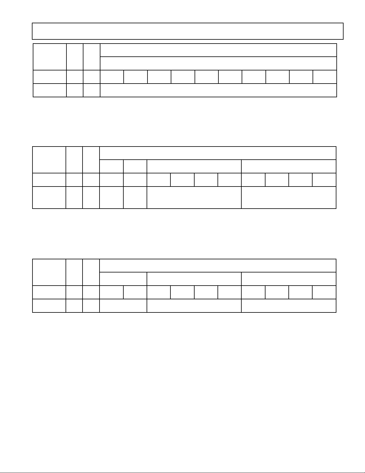
SSERDDARETSIGERW/RSERDLEIFATAD
5141312111019876543210
BSM=51tiB:etoN
Figure <ContPortMap>
SSERDDARETSIGERW/RSERDLEIFATAD
5141312111019876543210
0000 sgnitteSrewoP
0001 srediviDkcolC
0010 lortnoCtroPlaireS
0011 lortnoCetuM
0100 noitarugifnoCtuptuO/tupnI
01010 gnitteSniaG0CDA
0 1 0 1 1 leveLkaeP0CDA
PRELIMINARY TECHNICAL DA TA
01100 gnitteSniaG1CDA
0 1 1 0 1 leveLkaeP1CDA
0111 devreseR
1000 devreseR
100 1 tceleSretliFO/I
1010 gnitteSniaG0CAD
1011 gnitteSniaG1CAD
1100 devreseR
1101 devreseR
1110 lortnoCmirTFER
1111 lortnoCedoMtseT
PRELIMINARY
TECHNICAL
DATA
Figure <ContRegMap>
–16– Pr D 03/00
Page 17

PRELIMINARY TECHNICAL DA TA
AD74322
GER
W/RSER
SSERDDA
TESERARUPRUP1DUP0DUP3AUP2AUP1AUP0AUPUP
lortnoCrewoP
21-5111019876543210
rewoP
pU
0000
GER
W/RSER
SSERDDA
erawtfoS
teseR
-nerefeR
ec
-ifilpmA
re
rewoP
pU
-nerefeR
ec
Table <MCLK_Divider>
rewoP
pU
1CAD
rewoP
pU
0CAD
rewoP
pU
3CDA
rewoP
pU
2CDA
rewoP
pU
1CDA
srediviDkcolC
devreseR0-2DCB0-2DCM
rewoP
pU
0CDA
labolG
rewoP
pU
21-5111019876543210
0000
rediviDkcolCtiBrediviDkcolCretsaM
PRELIMINARY
TECHNICAL
DATA
GER
W/RSER
SSERDDA
-DTSD
EM
2SOPT1SOPT0SOPT1FDD0FDD1FDA0FDAMMSDSMSD
21-5111019876543210
MDT
0000
GER
W/RSER
SSERDDA
edoM
elbanE
MDT
edoM
noitisoP
2
1WWD0WWD1WWA0WWA
MDT
edoM
noitisoP
1
MDT
edoM
noitisoP
0
CAD
ataD
2tamroF
CAD
ataD
-UMD
1ET
21-5111019876543210
lortnoCecafretnIlaireS
CDA
2tamroF
ataD
2tamroF
CDA
ataD
1tamroF
--dexiM
edoM
elbanE
/retsaM
evalS
edoM
lortnoCetuM
-UMD
0ET
--
-UMA
1ET
-UMA
0ET
CAD
0000
droW
1htdiW
CAD
droW
0htdiW
CDA
droW
1htdiW
CDA
droW
0htdiW
–17–Pr D 03/00
etuM
1CAD
etuM
0CAD
devreseRdevreseR
etuM
1CDA
etuM
0CDA
Page 18

AD74322
GER
SSERDDA
21-5111019 8 7 6 5 4 3 2 1 0
W/RSER
PRELIMINARY TECHNICAL DA TA
noitarugifnoCCDA
-AEP
EK
SERBLDBLSD1BLA0BLA1VNI0VNI1EES0EES
CDA
1110
GER
W/RSER
SSERDDA
kaeP
leveL
gnidaeR
devreseR
latigiD
kcabpooL
ataD
TROPS
kcabpooL
golanA
kcabpooL
1hC
golanA
kcabpooL
0hC
trevnI
1CDA
stupnI
trevnI
0CDA
stupnI
kcabdaeRkaeP/gnitteSniaG0CDA
0-9G0A
ni1CDA
elgniS
dednE
edoM
21-5111019 8 7 6 5 4 3 2 1 0
10000
devreseR1G0A0G0A
1
PRELIMINARY
GER
W/RSER
SSERDDA
DATA
0-9G1A
TECHNICAL
kcabdaeRkaeP/gnitteSniaG1CDA
ni0CDA
elgniS
dednE
edoM
0P0AkcabdaeRkaeP0CDA9P0A
21-5111019 8 7 6 5 4 3 2 1 0
10000
1
GER
W/RSER
SSERDDA
devreseR1G1A0G1A
0P0AkcabdaeRkaeP1CDA9P1A
gnitteSniaG0CAD
0-9G0D
21-5111019876543210
1010
0G0DgnitteSniaG0CAD9G0D
–18– Pr D 03/00
Page 19
PRELIMINARY TECHNICAL DA TA
AD74322
GER
0110
GER
21-5111019876543210
0000
W/RSER
SSERDDA
21-5111019876543210
W/RSER
SSERDDA
FMBETL0-3TL0-3TS
wolB
retsaM
esuF
kniL
mirT
elbanE
mirTkniLmirTerawtfoS
gnitteSniaG1CAD
0-9G1D
0G1DgnitteSniaG1CAD9G1D
lortnoCmirT
PRELIMINARY
TECHNICAL
DATA
GER
0000
W/RSER
SSERDDA
21-5111019876543210
0-1EMT0-3ID0-3IA
lortnoCedoMtseTsgnitteStnerruCCADsgnitteStnerruCCDA
lortnoCedoMtseT
–19–Pr D 03/00
Page 20

AD74322
PRELIMINARY TECHNICAL DA TA
OUTLINE DIMENSIONS (STYLE: outline hd)
Dimensions shown in inches and (mm). (STYLE: outline sub)
00000000
PRELIMINARY
TECHNICAL
DATA
PRINTED IN U.S.A.
–20–
Pr D 03/00
 Loading...