

Page 1
10-Bit Digital Temperature Sensor
V
V
(AD7416) and Four Single-Channel ADCs
FEATURES
10-bit ADC with 15 μs and 30 μs conversion times
Single and 4 single-ended analog input channels
On-chip temperature sensor: −40°C to +125°C
On-chip track-and-hold
Overtemperature indicator
Automatic power-down at the end of a conversion
Wide operating supply range: 2.7 V to 5.5 V
2
I
C-compatible serial interface
Selectable serial bus address allows connection of up to 8
AD7416/AD7417 devices to a single bus
AD7416 is a superior replacement for LM75
APPLICATIONS
Data acquisition with ambient temperature monitoring
Industrial process control
Automotive
Battery-charging applications
Personal computers
GENERAL DESCRIPTION
The AD7417 and AD7418 are 10-bit, 4-channel and single-channel
ADCs with an on-chip temperature sensor that can operate from a
single 2.7 V to 5.5 V power supply. The devices contain a 15 μs
successive approximation converter, a 5-channel multiplexer, a
temperature sensor, a clock oscillator, a track-and-hold, and a
reference (2.5 V). The AD7416 is a temperature-monitoring only
device in an 8-lead package.
The temperature sensor on the parts can be accessed via multiplexer Channel 0. When Channel 0 is selected and a conversion
is initiated, the resulting ADC code at the end of the conversion
gives a measurement of the ambient temperature (±1°C @ 25°C).
On-chip registers can be programmed with high and low temperature limits, and an open-drain overtemperature indicator (OTI)
output is provided, which becomes active when a programmed
limit is exceeded.
A configuration register allows programming of the sense of the
OTI output (active high or active low) and its operating mode
(comparator or interrupt). A programmable fault queue counter
allows the number of out-of-limit measurements that must
occur before triggering the OTI output to be set to prevent
spurious triggering of the OTI output in noisy environments.
AD7416/AD7417/AD7418
FUNCTIONAL BLOCK DIAGRAMS
BAND GAP
TEMPERATURE
SENSOR
ADDRESS
POINTER
REGISTER
7
A0
6
A1
A2
5
TEMP
SENSOR
7
A
IN1
8
A
IN2
A
IN3
A
IN4
NC = NO CONNECT
A
MUX
9
10
1
16NC6
NC
DD
7
TEMP
SENSOR
5
MUX
IN
ANALOG-TO-DIGITAL
CONVERTER
TEMPERATURE
T
OTI
T
HYST
CONFIGURATION
Figure 1. AD7416
REF
IN
5
REF
2.5V
SAMPLING
CAPACITOR
V
BALANCE
GND
Figure 2. AD7417
REF
IN
6
REF
2.5V
SAMPLING
CAPACITOR
V
BALANCE
4
GND
Figure 3. AD7418
10-BIT
VAL UE
REGISTER
SETPOINT
REGISTER
SETPOINT
REGISTER
REGISTER
SERIAL BUS
INTERFACE
T
SETPOINT
OTI
REGIS TER
CHARGE
DISTRIBUTI ON
DAC
CLOCK
15
CONVST
T
SETPOINT
OTI
REGIS TER
CHARGE
DISTRIBUTI ON
DAC
CONTROL
CLOCK
8
CONVST
DD
14
CONTROL
LOGIC
LOGIC
AD7416
SETPOINT
COMPARATOR
FAULT
QUEUE
COUNTER
A > B
B
A
DATA OUT
2
I
C
INTERFACE
AD7417
13
12 11
A0
A1 A2
A > B
B
A
DATA OUT
2
I
C
INTERFACE
AD7418
8
V
DD
3
OTI
4
GND
SDA
1
2
SCL
01126-001
4
OTI
3
SCL
SDA
2
01126-002
3
OTI
2
SCL
SDA
1
01126-003
Rev. I
Information furnished by Analog Devices is believed to be accurate and reliable. However, no
responsibility is assumed by Anal og Devices for its use, nor for any infringements of patents or ot her
rights of third parties that may result from its use. Specifications subject to change without notice. No
license is granted by implication or otherwise under any patent or patent rights of Analog Devices.
Trademarks and registered trademarks are the property of their respective owners.
One Technology Way, P.O. Box 9106, Norwood, MA 02062-9106, U.S.A.
Tel: 781.329.4700 www.analog.com
Fax: 781.461.3113 ©1998–2010 Analog Devices, Inc. All rights reserved.
Page 2

AD7416/AD7417/AD7418
TABLE OF CONTENTS
Features.............................................................................................. 1
Applications....................................................................................... 1
General Description ......................................................................... 1
Functional Block Diagrams............................................................. 1
Revision History ............................................................................... 2
Product Highlights ........................................................................... 3
Specifications..................................................................................... 4
AD7417/AD7418 Specifications................................................. 4
AD7416 Specifications................................................................. 6
Absolute Maximum Ratings............................................................ 7
ESD Caution.................................................................................. 7
Pin Configurations and Function Descriptions ........................... 8
Terminology .................................................................................... 10
Theory of Operation ...................................................................... 11
Circuit Information.................................................................... 11
Converter Details........................................................................ 11
Typical Connection Diagram ................................................... 11
Analog Inputs.............................................................................. 11
REVISION HISTORY
11/10—Rev. H to Rev. I
Changes to Figure 19...................................................................... 16
2/09—Rev. G to Rev. H
Updated Format..................................................................Universal
Changes to Data Sheet Title, Figure 2 and Figure 3..................... 1
Moved Product Highlights Section................................................ 3
Changes to Table 1............................................................................ 4
Changes to Endnote 1, Table 2........................................................ 6
Added Figure 5 Caption................................................................... 7
Changes to Table 4............................................................................ 8
Changes to Table 5 and Table 6....................................................... 9
Changes to On-Chip Reference Section...................................... 11
Changes to Figure 13...................................................................... 12
Changes to Table 8 and Table 10................................................... 13
Changes to Figure 15, Figure 16, and Figure 17 ......................... 15
Changes to Reading Data From the AD7416/AD7417/AD7418
Section, Figure 18, and Figure 19 ................................................. 16
Change to Mode 1 .......................................................................... 17
Changes to Figure 22 Caption and
Section.............................................................................................. 18
Moved Figure 21 and Figure 22 .................................................... 18
Changes to Power-On Reset Section............................................ 19
Updated Outline Dimensions....................................................... 21
Changes to Ordering Guide.......................................................... 23
CONVST
Pin Mode
On-Chip Reference .................................................................... 11
Temperature Measurement....................................................... 12
Internal Register Structure........................................................ 12
Serial Bus Interface..................................................................... 14
OTI Output ................................................................................. 17
Fault Queue................................................................................. 17
Power-On Defaults..................................................................... 17
Operating Modes........................................................................ 17
CONVST
Applications Information.............................................................. 19
Supply Decoupling..................................................................... 19
Power-On Reset.......................................................................... 19
Mounting the AD7416/AD7417/AD7418 .............................. 19
Fan Controller............................................................................. 19
Thermostat.................................................................................. 19
System with Multiple AD7416 Devices................................... 20
Outline Dimensions....................................................................... 21
Ordering Guide .......................................................................... 23
8/04—Data Sheet Changed from Rev. F to Rev. G
Changes to Figure 12...................................................................... 12
Changes to Reading Data from the AD7416/AD7417/AD7418
Section.............................................................................................. 13
Changes to Power-On-Reset section ........................................... 14
7/03—Data Sheet Changed from Rev. E to Rev. F
Updated Features...............................................................................1
Updated Specifications .....................................................................3
Updated Absolute Maximum Ratings ............................................6
Updated Ordering Guide .................................................................6
Updated Product Highlights............................................................7
Updated Circuit Information...........................................................7
Updated Temperature Measurement section ................................9
10/02—Data Sheet Changed from Rev. D to Rev. E
Edits to Specifications Headings .....................................................2
Added Temperature Measurement section....................................8
Edits to Serial Bus Address section.............................................. 10
Edits to Figure 11............................................................................ 12
Edits to
Edits to Power-On-Reset section ................................................. 14
Addition of Figures 16 and 17 ...................................................... 15
Updated Outlines ........................................................................... 16
Start Mode................................................................. 18
CONVST
Pin Mode section ........................................... 14
Rev. I | Page 2 of 24
Page 3

AD7416/AD7417/AD7418
An I2C® compatible serial interface allows the AD7416/AD7417/
AD7418 registers to be written to and read back. The three
LSBs of the AD7416/AD7417 serial bus address can be selected,
which allows up to eight AD7416/AD7417 devices to be connected
to a single bus.
The AD7417 is available in a narrow body, 0.15 inch, 16-lead,
small outline package (SOIC) and in a 16-lead, thin shrink,
small outline package (TSSOP). The AD7416 and AD7418 are
available in 8-lead SOIC and MSOP packages.
PRODUCT HIGHLIGHTS
1. The AD7416/AD7417/AD7418 have an on-chip temperature
sensor that allows an accurate measurement of the ambient
temperature (±1°C @ 25°C, ±2°C overtemperature) to be
made. The measurable temperature range is −40°C to
+125°C. An overtemperature indicator is implemented by
carrying out a digital comparison of the ADC code for
Channel 0 (temperature sensor) with the contents of the
on-chip T
2. The AD7417 offers a space-saving, 10-bit analog-to-digital
solution with four external voltage input channels, an onchip temperature sensor, an on-chip reference, and a clock
oscillator.
3. The automatic power-down feature enables the AD7416/
AD7417/AD7418 to achieve superior power performance.
At slower throughput rates, the part can be programmed to
operate in a low power shutdown mode, allowing further
savings in power consumption.
setpoint register.
OTI
Rev. I | Page 3 of 24
Page 4

AD7416/AD7417/AD7418
SPECIFICATIONS
AD7417/AD7418 SPECIFICATIONS
VDD = 2.7 V to 5.5 V, GND = 0 V, REFIN = 2.5 V, unless otherwise noted.
Table 1.
Parameter A Version B Version1 Unit Test Conditions/Comments
DC ACCURACY Any channel
Resolution 10 10 Bits
Minimum Resolution for Which No
Missing Codes Are Guaranteed
Relative Accuracy2 ±1 ±1 LSB max This specification is typical for VDD of 3.6 V to 5.5 V
Differential Nonlinearity2 ±1 ±1 LSB max This specification is typical for VDD of 3.6 V to 5.5 V
Gain Error2 ±3 ±3 LSB max External reference
±10 ±10 LSB max Internal reference
Gain Error Match2 ±0.6 ±0.6 LSB max AD7417 only
Offset Error2 ±4 ±4 LSB max
Offset Error Match2 ±0.7 ±0.7 LSB max AD7417 only
ANALOG INPUTS
Input Voltage Range VREF VREF V max
0 0 V min
Input Leakage Current3 ±1 ±1 A max
Input Capacitance 10 10 pF max
TEMPERATURE SENSOR1
Measurement Error
Ambient Temperature 25°C ±2 ±1 °C max
T
to T
MIN
Temperature Resolution 1/4 1/4 °C/LSB
CONVERSION RATE
Track-and-Hold Acquisition Time4 400 400 ns max Source impedance < 10 Ω
Conversion Time
Temperature Sensor 30 30 s max Typically 27 s
Channel 1 to Channel 4 15 15 s max Typically 10 s
REFERENCE INPUT
REFIN Input Voltage Range 2.625 2.625 V max 2.5 V + 5%
2.375 2.375 V min 2.5 V − 5%
Input Impedance 40 40 kΩ min
Input Capacitance 10 10 pF max
ON-CHIP REFERENCE Nominal 2.5 V
Reference Error6 ±25 ±25 mV max
Temperature Coefficient6 80 80 ppm/°C typ
DIGITAL INPUTS
Input High Voltage, VIH VDD × 0.7 VDD × 0.7 V min
Input Low Voltage, VIL VDD × 0.3 VDD × 0.3 V max
Input Leakage Current 1 1 A max
DIGITAL OUTPUTS
Output Low Voltage, VOL 0.4 0.4 V max IOL = 3 mA
Output High Current 1 1 A max VOH = 5 V
±3 ±2 °C max
MAX
5, 6
10 10 Bits
Rev. I | Page 4 of 24
Page 5

AD7416/AD7417/AD7418
Parameter A Version B Version1 Unit Test Conditions/Comments
POWER REQUIREMENTS
VDD 5.5 5.5 V max For specified performance
2.7 2.7 V min
IDD Logic inputs = 0 V or VDD
Normal Operation 600 600 A max
Power-Down 1.5 1.5 A max 0.7 µA typically
Auto Power-Down Mode VDD = 3 V; see the Operating Modes section
10 SPS Throughput Rate 6 6 W typ
1 kSPS Throughput Rate 60 60 W typ
10 kSPS Throughput Rate 600 600 W typ
Power-Down 3 3 W max Typically 0.15 W
1
B Version applies to AD7417 only with temperature range of −40°C to +85°C. A Version temperature range is −40°C to +125°C. For VDD = 2.7 V, TA = 85°C maximum and
temperature sensor measurement error = ±3°C maximum.
2
See the Terminology section.
3
Refers to the input current when the part is not converting. Primarily due to reverse leakage current in the ESD protection diodes.
4
Sample tested during initial release and after any redesign or process change that may affect this parameter.
5
On-chip reference shuts down when an external reference is applied.
6
The accuracy of the temperature sensor is affected by reference tolerance.
Rev. I | Page 5 of 24
Page 6
AD7416/AD7417/AD7418
AD7416 SPECIFICATIONS
VDD = 2.7 V to 5.5 V, GND = 0 V, REFIN = 2.5 V, unless otherwise noted.
Table 2.
Parameter Min Typ Max Unit Test Conditions/Comments
TEMPERATURE SENSOR AND ADC
Accuracy ±2.0 °C TA = −25°C to + 100°C
(V
±3.0 °C TA = −40°C to + 125°C
(V
Resolution 10 Bits
Temperature Conversion Time 40 s
Update Rate, tR 400 s
OTI Delay 1 × tR 6 × tR ms Depends on fault queue setting
Supply Current 1.0 mA I2C active
350 600 A I2C inactive
0.2 1.5 A Shutdown mode
T
Default Temperature 80 °C
OTI
T
Default Temperature 75 °C
HYST
DIGITAL INPUTS
Input High Voltage, VIH VDD × 0.7 VDD + 0.5 V
Input Low Voltage, VIL −0.3 VDD × 0.3 V
Input High Current, IIH +0.005 +1.0 A VIN = 5 V
Input Low Current, IIL −0.005 −1.0 A VIN = 0 V
Input Capacitance, CIN 20 pF All digital inputs
DIGITAL OUTPUTS
Output Low Voltage, VOL 0.4 V IOL = 3 mA
Output High Current 1 A VOH = 5 V
Output Fall Time, tf 250 ns CL = 400 pF, IO = 3 mA
OS Output Low Voltage, VOL 0.8 V I
AC ELECTRICAL CHARACTERISTICS2 AD7416/AD7417/AD7418
Serial Clock Period, t1 2.5 s See Figure 4
Data In Setup Time to SCL High, t2 50 ns See Figure 4
Data Out Stable after SCL Low, t3 0 ns See Figure 4
SDA Low Setup Time to SCL Low
(Start Condition), t4 50 ns See Figure 4
SDA High Hold Time after SCL High
(Stop Condition), t5 50 ns See Figure 4
SDA and SCL Fall Time, t6 300 ns See Figure 4
1
For VDD = 2.7 V to 3 V, TA maximum = 85°C and temperature sensor measurement error = ±3°C maximum.
2
Sample tested during initial release and after any redesign or process change that may affect this parameter.
t
1
SCL
= 3 V minimum)1
DD
= 3 V minimum)1
DD
= 4 mA
OUT
SDA
DATA IN
SDA
DATA OUT
t
4
t
2
t
3
t
5
t
6
01126-004
Figure 4. Diagram for Serial Bus Timing
Rev. I | Page 6 of 24
Page 7
AD7416/AD7417/AD7418
V
ABSOLUTE MAXIMUM RATINGS
TA = 25°C, unless otherwise noted.
Table 3.
Parameter Rating
VDD to AGND −0.3 V to +7 V
VDD to DGND −0.3 V to +7 V
Analog Input Voltage to AGND
A
to A
IN1
−0.3 V to VDD + 0.3 V
IN4
Reference Input Voltage to AGND1 −0.3 V to VDD + 0.3 V
Digital Input Voltage to DGND −0.3 V to VDD + 0.3 V
Digital Output Voltage to DGND −0.3 V to VDD + 0.3 V
Operating Temperature Range
A Version −40°C to +125°C
B Version −40°C to +85°C
Storage Temperature Range −65°C to +150°C
Junction Temperature 150°C
TSSOP, Power Dissipation 450 mW
θJA Thermal Impedance 120°C/W
Lead Temperature, Soldering 260°C
Vapor Phase (60 sec) 215°C
Infrared (15 sec) 220°C
16-Lead SOIC Package, Power Dissipation 450 mW
θJA Thermal Impedance 100°C/W
Lead Temperature, Soldering
Vapor Phase (60 sec) 215°C
Infrared (15 sec) 220°C
8-Lead SOIC Package, Power Dissipation 450 mW
θJA Thermal Impedance 157°C/W
Lead Temperature, Soldering
Vapor Phase (60 sec) 215°C
Infrared (15 sec) 220°C
MSOP Package, Power Dissipation 450 mW
θJA Thermal Impedance 206°C/W
Lead Temperature, Soldering
Vapor Phase (60 sec) 215°C
Infrared (15 sec) 220°C
1
If the reference input voltage is likely to exceed VDD by more than 0.3 V (for
example, during power-up) and the reference is capable of supplying 30 mA
or more, it is recommended to use a clamping diode between the REFIN pin
and the V
pin. Figure 5 shows how the diode should be connected.
DD
Stresses above those listed under Absolute Maximum Ratings
may cause permanent damage to the device. This is a stress
rating only; functional operation of the device at these or any
other conditions above those indicated in the operational
section of this specification is not implied. Exposure to absolute
maximum rating conditions for extended periods may affect
device reliability.
REF
IN
AD7417
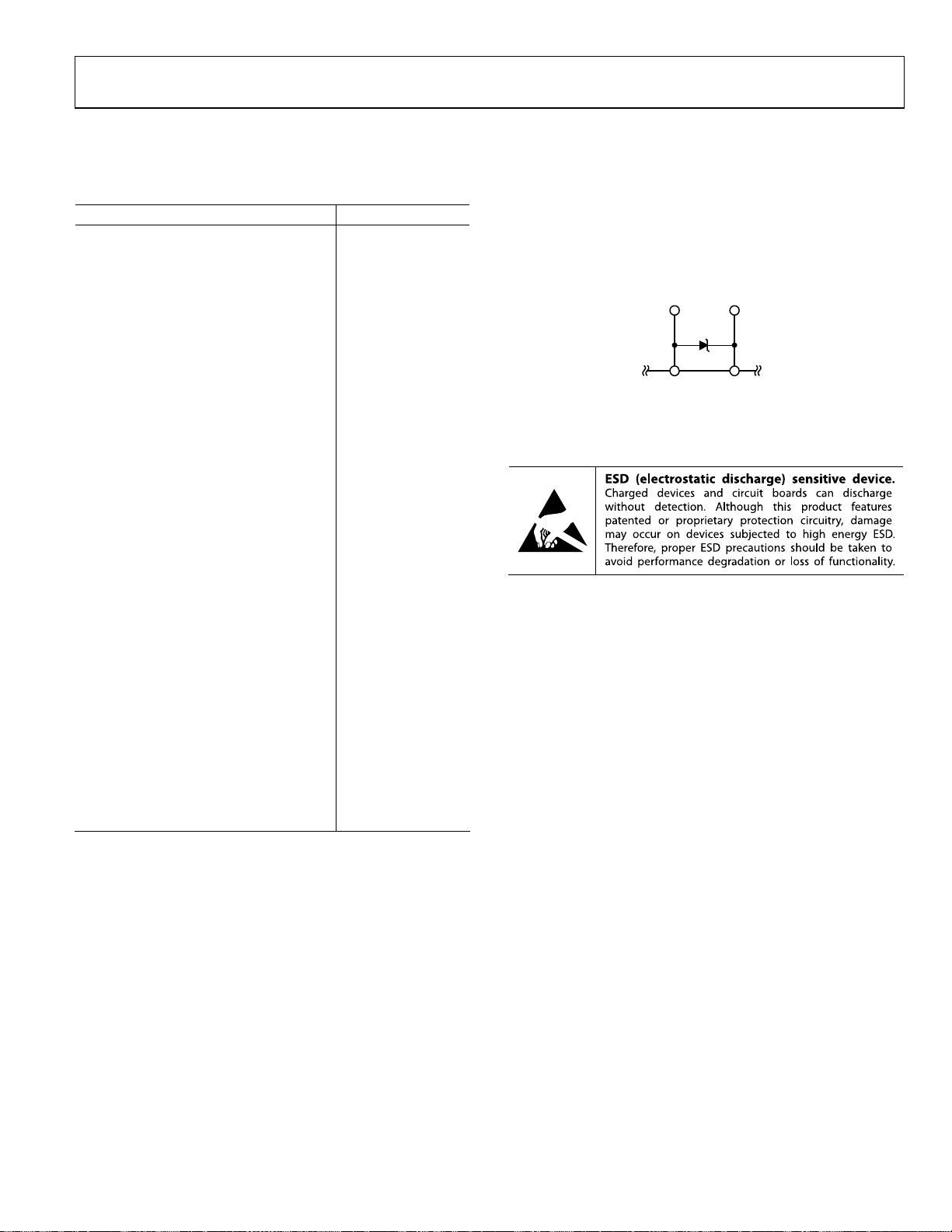
Figure 5. Diode Connection
BAT81
DD
01126-025
ESD CAUTION
Rev. I | Page 7 of 24
Page 8
AD7416/AD7417/AD7418
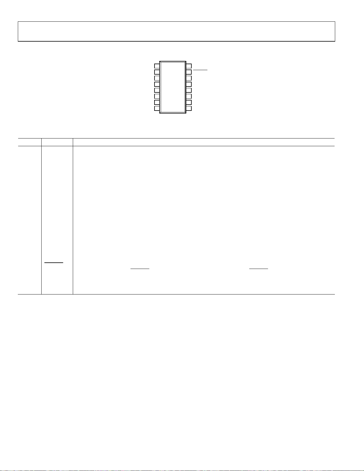
PIN CONFIGURATIONS AND FUNCTION DESCRIPTIONS
NC
1
SDA
2
SCL
3
AD7417
4
OTI
TOP VIEW
5
IN
GND
6
A
7
IN1
8
A
IN2
NC = NO CONNECT
(Not to Scale)
REF
Figure 6. AD7417 Pin Configuration (SOIC/TSSOP)
Table 4. AD7417 Pin Function Descriptions
Pin No. Mnemonic Description
1, 16 NC No Connection. Do not connect anything to this pin.
2 SDA Digital I/O. Serial bus bidirectional data. Push-pull output.
3 SCL Digital Input. Serial bus clock.
4 OTI
This pin is a logic output. The overtemperature indicator (OTI) is set if the result of a conversion on Channel 0
(temperature sensor) is greater than an 8-bit word in the T
serial read operation. Open-drain output.
5 REFIN
Reference Input. An external 2.5 V reference can be connected to the AD7417 at this pin. To enable the on-chip
reference, the REF
pin should be tied to GND. If an external reference is connected to the AD7417, the internal
IN
reference shuts down.
6 GND Ground reference for track-and-hold, comparator and capacitor DAC, and digital circuitry.
7 to 10 A
IN1
to A
Analog Input Channels. The AD7417 has four analog input channels. The input channels are single-ended with
IN4
respect to GND. The input channels can convert voltage signals in the range of 0 V to VREF. A channel is selected by
writing to the configuration register of the AD7417.
11 A2 Digital Input. This is the highest programmable bit of the serial bus address.
12 A1 Digital Input. This is the middle programmable bit of the serial bus address.
13 A0 Digital Input. This is the lowest programmable bit of the serial bus address.
14 VDD Positive Supply Voltage, 2.7 V to 5.5 V.
15
CONVST
Logic Input Signal. Convert start signal. The rising edge of this signal fully powers up the part. The power-up time
for the part is 4 s. If the CONVST pulse is greater than 4 s, the falling edge of CONVST places the track-and-hold
mode into hold mode and initiates a conversion. If the pulse is less than 4 s, an internal timer ensures that the
track-and-hold does not go into hold, and conversion is not initiated until the power-up time has elapsed. The
track-and-hold goes into track mode again at the end of conversion (see the section). Operating Modes
16
15
14
13
12
11
10
9
NC
CONVST
V
DD
A0
A1
A2
A
IN4
A
IN3
01126-005
setpoint register. The signal is reset at the end of a
OTI
Rev. I | Page 8 of 24
Page 9

AD7416/AD7417/AD7418
SDA
1
OTI
AD7416
2
3
TOP VIEW
(Not to Scal e)
4
SCL
GND
Figure 7. AD7416 Pin Configuration (SOIC/MSOP) Figure 8. AD7418 Pin Configuration (SOIC/MSOP)
Table 5. AD7416 Pin Function Descriptions
Pin No. Mnemonic Description
1 SDA Digital I/O. Serial bus bidirectional data. Push-pull output.
2 SCL Digital Input. Serial bus clock.
3 OTI
This pin is a logic output. The OTI is set if the result of a conversion on Channel 0 (temperature sensor) is greater
than an 8-bit word in the T
output.
4 GND Ground reference for track-and-hold, comparator and capacitor DAC, and digital circuitry.
5 A2 Digital Input. This is the highest programmable bit of the serial bus address.
6 A1 Digital Input. This is the middle programmable bit of the serial bus address.
7 A0 Digital Input. This is the lowest programmable bit of the serial bus address.
8 VDD Positive Supply Voltage, 2.7 V to 5.5 V.
Table 6. AD7418 Pin Function Descriptions
Pin No. Mnemonic Description
1 SDA Digital I/O. Serial bus bidirectional data. Push-pull output.
2 SCL Digital Input. Serial bus clock.
3 OTI
This is a logic output. The OTI is set if the result of a conversion on Channel 0 (temperature sensor) is greater than
an 8-bit word in the T
output.
4 GND Ground reference for track-and-hold, comparator and capacitor DAC, and digital circuitry.
5 AIN
Analog Input Channel. The input channel is single-ended with respect to GND. The input channel can convert
voltage signals in the range of 0 V to VREF. The analog input channel is selected by writing to the configuration
register of the AD7418 and choosing Channel 4.
6 REFIN
Reference Input. An external 2.5 V reference can be connected to the AD7418 at this pin. To enable the on-chip
reference, the REF
reference shuts down.
7 VDD Positive Supply Voltage, 2.7 V to 5.5 V.
CONVST
8
Logic Input Signal. Convert start signal. The rising edge of this signal fully powers up the part. The power-up time
for the part is 4 s. If the
mode into hold mode and initiates a conversion. If the pulse is less than 4 s, an internal timer ensures that the
track-and-hold does not go into hold, and conversion is not initiated until the power-up time has elapsed. The
track-and-hold goes into track mode again at the end of conversion (see the section). Operating Modes
V
8
DD
A0
7
6
A1
5
A2
1126 -0 06
setpoint register. The signal is reset at the end of a serial read operation. Open-drain
OTI
setpoint register. The signal is reset at the end of a serial read operation. Open-drain
OTI
pin should be tied to GND. If an external reference is connected to the AD7418, the internal
IN
CONVST
pulse is greater than 4 s, the falling edge of
SDA
SCL
OTI
GND
1
AD7418
2
3
TOP VIEW
(Not to Scale)
4
CONVST
CONVST
8
V
7
DD
6
REF
IN
5
A
IN
01126-007
places the track-and-hold
Rev. I | Page 9 of 24
Page 10

AD7416/AD7417/AD7418
TERMINOLOGY
Relative Accuracy
Relative accuracy or endpoint nonlinearity is the maximum
deviation from a straight line passing through the endpoints of
the ADC transfer function.
Differential Nonlinearity
This is the difference between the measured and the ideal 1 LSB
change between any two adjacent codes in the ADC.
Offset Error
This is the deviation of the first code transition (0000…000) to
(0000…001) from the ideal, that is, GND + 1 LSB.
Offset Error Match
This is the difference in offset error between any two channels.
Gain Error
This is the deviation of the last code transition (1111…110) to
(1111…111) from the ideal, that is, VREF − 1 LSB, after the
offset error has been adjusted out.
Gain Error Match
This is the difference in gain error between any two channels.
Track-and-Hold Acquisition Time
Track-and-hold acquisition time is the time required for the
output of the track-and-hold amplifier to reach its final value,
within ±½ LSB, after the end of conversion (the point at which
the track-and-hold returns to track mode). It also applies to
situations where a change in the selected input channel takes
place or where there is a step input change on the input voltage
applied to the selected A
means that the user must wait for the duration of the track-andhold acquisition time after the end of conversion, or after a
channel change or step input change to A
another conversion, to ensure that the part operates to
specification.
input of the AD7417 or AD7418. It
IN
before starting
IN
Rev. I | Page 10 of 24
Page 11

AD7416/AD7417/AD7418
V
A
THEORY OF OPERATION
CIRCUIT INFORMATION
The AD7417 and AD7418 are single-channel and four-channel,
15 μs conversion time, 10-bit ADCs with on-chip temperature
sensor, reference, and serial interface logic functions on a single
chip. The AD7416 has no analog input channel and is intended
for temperature measurement only. The ADC section consists
of a conventional successive approximation converter based
around a capacitor DAC. The AD7416, AD7417, and AD7418
are capable of running on a 2.7 V to 5.5 V power supply, and the
AD7417 and AD7418 accept an analog input range of 0 V to
+VREF. The on-chip temperature sensor allows an accurate
measurement of the ambient device temperature to be made.
The working measurement range of the temperature sensor is
−40°C to +125°C. The parts require a 2.5 V reference that can
be provided from the part’s own internal reference or from an
external reference source.
CONVERTER DETAILS
Conversion is initiated on the AD7417/AD7418 by pulsing the
CONVST
input. The conversion clock for the part is internally
generated so that no external clock is required except when
reading from and writing to the serial port. The on-chip trackand-hold goes from track mode to hold mode, and the conversion
sequence is started on the falling edge of the
CONVST
signal.
A conversion is also initiated in the automatic conversion mode
every time a read or write operation to the AD7416/AD7417/
AD7418 takes place. In this case, the internal clock oscillator
(which runs the automatic conversion sequence) is restarted
at the end of the read or write operation. The track-and-hold
goes into hold mode approximately 3 μs after the read or write
operation is complete, and a conversion is then initiated. The
result of the conversion is available either 15 μs or 30 μs later,
depending on whether an analog input channel or the temperature sensor is selected. The track-and-hold acquisition time of
the AD7417/AD7418 is 400 ns.
A temperature measurement is made by selecting the Channel 0
of the on-chip mux and carrying out a conversion on this
channel. A conversion on Channel 0 takes 30 μs to complete.
Temperature measurement is explained in the Temperature
Measurement section.
The on-chip reference is not available to the user, but REF
IN
can
be overdriven by an external reference source (2.5 V only).
All unused analog inputs should be tied to a voltage within the
nominal analog input range to avoid noise pickup. For
minimum power consumption, the unused analog inputs
should be tied to GND.
TYPICAL CONNECTION DIAGRAM
Figure 9 shows a typical connection diagram for the AD7417.
Using the A0, A1, and A2 pins allows the user to select from up
to eight AD7417 devices on the same serial bus, if desired. An
external 2.5 V reference can be connected at the REF
pin. If an
IN
Rev. I | Page 11 of 24
external reference is used, a 10 μF capacitor should be connected
between REF
and GND. SDA and SCL form the 2-wire I2C
IN
compatible interface. For applications where power consumption is of concern, the automatic power-down at the end of a
conversion should be used to improve power performance (see
the Operating Modes section.)
SUPPLY
2.7V TO 5. 5V
0V TO 2.5V
OPTIONAL
EXTERNAL
REFERENCE
INPUT
AD780/
REF192
+ +
A
A
A
A
GND
0.1µF10µF
IN1
IN2
IN3
IN4
V
DD
AD7417
REF
INTERFACE
SCL
SDA
CONVST
OTI
A0
A1
A2
IN
10µF FOR
EXTERNAL
REFERENCE
2-WIRE
SERIAL
MICROCONTROLLER/
MICROPRO CESSOR
Figure 9. Typical AD7417 Connection Diagram
ANALOG INPUTS
Figure 10 shows an equivalent circuit of the analog input
structure of the AD7417 and AD7418. The two diodes, D1
and D2, provide ESD protection for the analog inputs. Care
must be taken to ensure that the analog input signal never
exceeds the supply rails by more than 200 mV to prevent these
diodes from becoming forward-biased and start conducting
current into the substrate. The maximum current these diodes
can conduct without causing irreversible damage to the part is
20 mA. Capacitor C2 in Figure 10 is typically about 4 pF and
can primarily be attributed to pin capacitance. Resistor R1 is a
lumped component made up of the on resistance of a multiplexer
and a switch. This resistor is typically about 1 kΩ. Capacitor C1
is the ADC sampling capacitor and has a capacitance of 3 pF.
DD
D1
IN
4pF
C2
D2
R1
1kΩ
CONVERT PHASE: SWITCH OPEN
TRACK PHASE: SWI TCH CLOSED
Figure 10. Equivalent Analog Input Circuit
C1
3pF
V
BALANCE
01126-009
ON-CHIP REFERENCE
The AD7417/AD7418 have an on-chip 1.2 V band gap reference
that is amplified by a switched capacitor amplifier to give an
output of 2.5 V. The amplifier is only powered up at the start of
the conversion phase and is powered down at the end of the
conversion. The on-chip reference is selected by connecting the
REF
pin to analog ground, which causes SW1 (see Figure 11) to
IN
open and the reference amplifier to power up during a conversion. Therefore, the on-chip reference is not available externally.
01126-008
Page 12

AD7416/AD7417/AD7418
V
An external 2.5 V reference can be connected to the REFIN pin.
This has the effect of shutting down the on-chip reference
circuitry.
REF
1.2V
SW1
IN
26kΩ
24kΩ
1.2V
2.5V
EXTERNAL
REFERENCE
DETECT
BUFFER
Figure 11. On-Chip Reference
TEMPERATURE MEASUREMENT
A common method of measuring temperature is to exploit the
negative temperature coefficient of a diode, or the base-emitter
voltage of a transistor, operated at a constant current. Unfortunately, this technique requires calibration to null out the effect
of the absolute value of V
The technique used in the AD7416/AD7417/AD7418 is to
measure the current change in V
at two different currents.
This is given by
BE
where:
K is Boltzmann’s constant.
q is the charge on the electron (1.6 × 10
T is the absolute temperature in Kelvins.
N is the ratio of the two currents.
IN × I
SENSING
TRANSISTOR
Figure 12. Temperature Measurement Technique
Figure 12 shows the method the AD7416/AD7417/AD7418 use
to measure the device temperature. To measure ΔV
sensor (substrate transistor) is switched between operating
currents of I and N × I. The resulting waveform is passed through
a chopper-stabilized amplifier that performs the functions of
amplification and rectification of the waveform to produce a dc
voltage proportional to ΔV
to give a temperature output in 10-bit twos complement form.
, which varies from device to device.
BE
when the device is operated
BE
()
NqKTV
n1/ ×=Δ
−19
Coulombs).
DD
SENSING
TRANSISTOR
BE
. This voltage is measured by the ADC
BE
, the
V
OUT+
TO ADC
V
OUT–
Rev. I | Page 12 of 24
1126-010
01126-011
The temperature resolution of the ADC is 0.25°C, which corresponds to 1 LSB of the ADC. The ADC can theoretically measure a
temperature span of 255°C; the guaranteed temperature range is
−40°C to +125°C. The result of the conversion is stored in the
temperature value register (0x00) as a 16-bit word. The 10 MSBs
of this word store the temperature measurement (see Tabl e 9
and Tabl e 10 ).
The temperature conversion formulas using the 10 MSBs of the
temperature value register are
Positive Temperature = ADC Code/4 (1)
Negative Temperature = (ADC Code − 512)/4 (2)
The MSB is removed from ADC Code in Equation 2.
INTERNAL REGISTER STRUCTURE
The AD7417/AD7418 have seven internal registers, as shown in
Figure 13. Six of these are data registers and one is an address
pointer register. The AD7416 has five internal registers (the
ADC and Config2 registers are not applicable to the AD7416).
TEMPERATURE
VAL UE
REGISTER
(READ-ONLY
ADDRESS 0x00)
CONFIGURATION
REGISTER
(READ/WRIT E
ADDRESS 0x01)
T
SETPOINT
HYST
ADDRESS POINT ER
REGISTER
(SELCTS DATA REGISTER
FOR READ /WRI TE)
ADDRESS
SERIAL BUS INTERFACE
Figure 13. AD7417/AD7418 Register Structure
Address Pointer Register
The address pointer register is an 8-bit register that stores an
address that points to one of the six data registers. The first data
byte of every serial write operation to the AD7416/AD7417/
AD7418 is the address of one of the data registers, which is
stored in the address pointer register, and selects the data
register to which subsequent data bytes are written. Only the
three LSBs of the address pointer register are used to select a
data register.
Table 7. Address Pointer Register
P71 P61 P51 P41 P31 P2 P1 P0
0 0 0 0 0 Register select
1
P3 to P7 must be set to 0.
REGISTER
(READ/WRIT E
ADDRESS 0x02)
T
SETPOINT
OTI
REGISTER
(READ/WRIT E
ADDRESS 0x03)
ADC VALUE
REGISTER
(READ-ONLY
ADDRESS 0x04)
CONFIG2
REGISTER
(READ/WRIT E
ADDRESS 0x05)
DATA
SDA
SCL
01126-012
Page 13

AD7416/AD7417/AD7418
Table 8. Register Addresses
P2 P1 P0 Registers
0 0 0 Temperature value
0 0 1 Configuration register
0 1 0 T
0 1 1 T
setpoint
HYST
setpoint
OTI
1 0 0 ADC value (AD7417/AD7418 only)
1 0 1 Config2 (AD7417/AD7418 only)
Temperature Value Register (Address 0x00)
The temperature value register is a 16-bit, read-only register
whose 10 MSBs store the temperature reading from the ADC in
10-bit twos complement format. Bit D5 to Bit D0 are unused.
Table 9. Temperature Value Register
D15 D14 D13 D12 D11 D10 D9 D8 D7 D6
MSB B8 B7 B6 B5 B4 B3 B2 B1 LSB
The temperature data format is shown in Tabl e 10 . This shows
the full theoretical range of the ADC from −128°C to +127°C,
but in practice, the temperature measurement range is limited
to the operating temperature range of the device.
Table 10. Temperature Data Format
Temperature Digital Output
−128°C 10 0000 0000
−125°C 10 0000 1100
−100°C 10 0111 0000
−75°C 10 1101 0100
−50°C 11 0011 1000
−25°C 11 1001 1100
−10°C 11 1101 1000
−0.25°C 11 1111 1111
0°C 00 0000 0000
+0.25°C 00 0000 0001
+10°C 00 0010 1000
+25°C 00 0110 0100
+50°C 00 1100 1000
+75°C 01 0010 1100
+100°C 01 1001 0000
+125°C 01 1111 0100
+127°C 01 1111 1100
Configuration Register (Address 0x01)
The configuration register is an 8-bit, read/write register that is
used to set the operating modes of the AD7416/AD7417/AD7418.
Bit D7 to Bit D5 control the channel selection as outlined in
Tabl e 1 2 . Bits[D7:D5] should always be set to 000 for the AD7416.
Bit D4 and Bit D3 are used to set the length of the fault queue.
D2 sets the sense of the OTI output. D1 selects the comparator
or interrupt mode of operation, and D0 = 1 selects the shutdown
mode (default: D0 = 0).
Table 11. Configuration Register
D7 D6 D5 D4 D3 D2 D1 D0
Channel
selection
Fault
queue
OTI
polarity
Cmp/Int Shutdown
Rev. I | Page 13 of 24
The AD7416 contains a temperature-only channel; the AD7417
has four analog input channels and a temperature channel; and
the AD7418 has two channels, a temperature channel, and an
analog input channel. The temperature channel address for all
parts is the same, Channel 0. The address for the analog input
channel on the AD7418 is Channel 4. Tabl e 12 outlines the
channel selection on the parts, and Ta b le 1 3 shows the fault
queue settings. D1 and D2 are explained in the OTI Output
section.
Table 12. Channel Selection
D7 D6 D5 Channel Selection
0 0 0 Temperature sensor (all parts), Channel 0
0 0 1 A
0 1 0 A
0 1 1 A
1 0 0 A
(AD7417 only), Channel 1
IN1
(AD7417 only), Channel 2
IN2
(AD7417 only), Channel 3
IN3
(AD7417) and AIN (AD7418), Channel 4
IN4
Table 13. Fault Queue Settings
D4 D3 Number of Faults
0 0 1 (power-up default)
0 1 2
1 0 4
1 1 6
T
Setpoint Register (Address 0x02)
HYST
The T
nine MSBs store the T
setpoint register is a 16-bit, read/write register whose
HYST
setpoint in twos complement format
HYST
equivalent to the nine MSBs of the temperature value register.
Bit D6 to Bit D0 are unused.
T
Setpoint Register (Address 0x03)
OTI
The T
nine MSBs store the T
setpoint register is a 16-bit, read/write register whose
OTI
setpoint in twos complement format
OTI
equivalent to the nine MSBs of the temperature value register.
Bit 6 to Bit 0 are unused.
Table 14. T
Setpoint and T
HYST
Setpoint Registers
OTI
D15 D14 D13 D12 D11 D10 D9 D8 D7
MSB B7 B6 B5 B4 B3 B2 B1 LSB
ADC Value Register (Address 0x04)
The ADC value register is a 16-bit, read-only register whose
10 MSBs store the value produced by the ADC in binary format.
Bit D5 to Bit D0 are unused. Tabl e 15 shows the ADC value
register with 10 MSBs containing the ADC conversion request.
Table 15. ADC Value Register
D15 D14 D13 D12 D11 D10 D9 D8 D7 D6
MSB B8 B7 B6 B5 B4 B3 B2 B1 LSB
ADC Transfer Function
The designed code transitions occur at successive integer
LSB values (that is, 1 LSB, 2 LSB, and so on). The LSB size =
VREF/1024. The ideal transfer function characteristic for the
AD7417 and AD7418 ADC is shown in Figure 14.
Page 14

AD7416/AD7417/AD7418
direction of the data transfer, that is, whether data is written
111.. .111
111.. .110
111...000
011...111
ADC CODE
000...010
000...001
000...000
0V 1/2LSB
Figure 14. Ideal Transfer Function Characteristic for the AD7417/AD7418
1LSB – VREF /1024
+VREF – 1LSB
ANALOG INPUT
01126-013
Config2 Register (Address 0x05)
A second configuration register is included in the AD7417/
AD7418 for the functionality of the
CONVST
pin. It is an 8-bit
register with Bit D5 to Bit D0 being left at 0. Bit D7 determines
whether the AD7417/AD7418 should be operated in its default
mode (D7 = 0), performing conversions every 355 μs or in its
CONVST
when the
When this bit is 0, the I
pin mode (D7 = 1), where conversions start only
CONVST
pin is used. Bit 6 contains the Test 1 bit.
2
C filters are enabled (default). Setting
this bit to 1 disables the filters.
Table 16. Config2 Register
D7 D6 D5 D4 D3 D2 D1 D0
Conversion mode Test 1 0 0 0 0 0 0
SERIAL BUS INTERFACE
Control of the AD7416/AD7417/AD7418 is carried out via the
2
C compatible serial bus. The AD7416/AD7417/AD7418 are
I
connected to this bus as a slave device, under the control of a
master device, for example, the processor.
Serial Bus Address
As with all I2C compatible devices, the AD7416/AD7417/AD7418
have a 7-bit serial address. The four MSBs of this address for the
AD7416 are set to 1001; the AD7417 are set to 0101, and the
three LSBs can be set by the user by connecting the A2 to A0
pins to either V
up to eight AD7416/AD7417 devices can be connected to a
single serial bus, or the addresses can be set to avoid conflicts
with other devices on the bus. The four MSBs of this address for
the AD7418 are set to 0101, and the three LSBs are all set to 0.
If a serial communication occurs during a conversion operation,
the conversion stops and restarts after the communication.
The serial bus protocol operates as follows:
1. The master initiates data transfer by establishing a start condi-
tion, defined as a high-to-low transition on the serial data
line, SDA, while the serial clock line, SCL, remains high.
This indicates that an address/data stream follows. All slave
peripherals connected to the serial bus respond to the 7-bit
address (MSB first) plus an R/
or GND. By giving them different addresses,
DD
W
bit, which determines the
to or read from the slave device.
The peripheral whose address corresponds to the transmitted
address responds by pulling the data line low during the low
period before the ninth clock pulse, known as the acknowledge bit. All other devices on the bus now remain idle while
the selected device waits for data to be read from or written
to it. If the R/
slave device. If the R/
W
bit is a 0, then the master writes to the
W
bit is a 1, then the master reads
from the slave device.
2. Data is sent over the serial bus in sequences of nine clock
pulses, eight bits of data followed by an acknowledge bit
from the receiver of data. Transitions on the data line must
occur during the low period of the clock signal and remain
stable during the high period, because a low-to-high transition when the clock is high may be interpreted as a stop signal.
3. When all data bytes have been read or written, stop
conditions are established. In write mode, the master pulls
the data line high during the 10th clock pulse to assert a
stop condition. In read mode, the master device pulls the
data line high during the low period before the ninth clock
pulse. This is known as no acknowledge. The master then
takes the data line low during the low period before the
10th clock pulse, then high during the 10th clock pulse to
assert a stop condition.
Any number of bytes of data can be transferred over the serial
bus in one operation, but it is not possible to mix read and write
in one operation because the type of operation is determined at
the beginning and cannot subsequently be changed without
starting a new operation.
Writing to the AD7416/AD7417/AD7418
Depending on the register being written to, there are three
different writes for the AD7416/AD7417/AD7418.
• Writing to the address pointer register for a subsequent read.
To read data from a particular register, the address pointer
register must contain the address of that register. If it does
not, the correct address must be written to the address pointer
register by performing a single-byte write operation, as shown
in Figure 15. The write operation consists of the serial bus
address followed by the address pointer byte. No data is
written to any of the data registers.
• Writing a single byte of data to the configuration register, the
Config2 register, or to the T
setpoint or T
OTI
setpoint
HYST
registers.
The configuration register is an 8-bit register, so only one
byte of data can be written to it. If only 8-bit temperature
comparisons are required, the temperature LSB can be
ignored in T
written to the T
and T
OTI
setpoint and T
OTI
, and only eight bits need to be
HYST
setpoint registers.
HYST
Writing a single byte of data to one of these registers consists
of the serial bus address, the data register address written
to the address pointer register, followed by the data byte
Rev. I | Page 14 of 24
Page 15

AD7416/AD7417/AD7418
S
written to the selected data register. This is illustrated in
Figure 16.
• Writing two bytes of data to the T
setpoint or T
OTI
setpoint register.
If 9-bit resolution is required for the temperature setpoints,
two bytes of data must be written to the T
setpoint and
OTI
1 19 9
SCL
HYST
setpoint registers. This consists of the serial bus
T
HYST
address, the register address written to the address pointer
register, followed by two data bytes written to the selected
data register. This is illustrated in Figure 17.
DA 1001
START BY
MASTER
1
AD741x = AD7416/AD7417/AD7418.
Figure 15. Writing to the Address Pointer Register to Select a Data Register for a Subsequent Read Operation
1 1
SCL
SDA 1 0 0 1
START BY
MASTER
1
AD741x = AD7416/AD7417/AD7418.
Figure 16. Writing to the Address Pointer Register Followed by a Single Byte of Data to the Selected Data Register
A2 A1 P7 P6 P5 P4 P3 P2 P1 P0A0 R/ W
FRAME 1
SERIAL BUS ADDRESS BYTE
A2 A1 P7 P6 P5 P4 P3 P2 P1 P0
FRAME 1
SERIAL BUS ADDRESS BYTE
SCL (CONTINUED)
SDA (CONTINUED)
ACK. BY
AD741x
A0 R/ W
1
9
ACK. BY
AD741x
1
ADDRESS POINTE R REGISTER BYT E
1
D6D7 D5 D4 D3 D2 D1 D0
FRAME 2
FRAME 3
DATA BYTE
FRAME 2
ADDRESS POINTE R REGISTE R BYTE
ACK. BY
AD741x
9
ACK. BY
AD741x
9
ACK. BY
AD741x
MASTER
1
1
MASTER
STOP
BY
STOP
BY
1
01126-014
01126-015
119
SCL
SDA 1 0 0 1
START BY
MASTER
SERIAL BUS ADDRESS BYTE
SCL
(CONTINUED)
SDA
(CONTINUED)
1
AD741x = AD7416/AD7417/AD7418.
D15 D14 D13 D12 D 11 D10 D9 D8 D7 D6 D5 D4 D3 D2 D1 D0
Figure 17. Writing to the Address Pointer Register Followed by Two Bytes of Data to the T
A2
A1 P7 P6 P5 P4 P3 P2 P1 P0A0 R /W
FRAME 1
MOST SIG NIFICANT DATA BYTE
FRAME 3
ACK. BY
AD741x
ACK. BY
AD741x
1
ADDRESS POINT ER REGISTE R BYTE
119
STOP BY
1
MASTER
FRAME 2
LEAST SIGNIFICANT DATA BYTE
FRAME 4
Setpoint or T
OTI
HYST
9
ACK. BY
1
AD741x
9
ACK. BY
AD741x
Setpoint Register
1
STOP
BY
MASTER
01126-016
Rev. I | Page 15 of 24
Page 16

AD7416/AD7417/AD7418
S
S
Reading Data From the AD7416/AD7417/AD7418
Reading data from the AD7416/AD7417/AD7418 is a singlebyte or 2-byte operation. Reading back the contents of the
configuration register is a single-byte read operation, as shown
in Figure 18, with the register address previously having been
set by a single-byte write operation to the address pointer
register.
Reading data from the temperature value register, the T
setpoint or T
setpoint register is a 2-byte operation, as
HYST
OTI
shown in Figure 19. It is also possible to read the most
significant bit of a 9-bit or 10-bit register in this manner.
1 19 9
SCL
Note that when reading back from the AD7416/AD7417/
AD7418, no more than three bytes of data must be read back.
A stop command must be inserted at the end of the read
communication. If a stop command is not inserted by the
master and the AD7416/AD7417/AD7418 receive more SCL
cycles than the maximum needed for three bytes of data, then
2
the I
C interface on the AD7416/AD7417/AD7418 pulls the
SDA line low and prevents it from going high again. To recover
the AD7416/AD7417/AD7418 interface, the part must be
powered off and on again. Reference the AN-686 Application
Note, Implementing an I
information on I
2
2
C® Reset at www.analog.com for more
C interfaces.
DA 1 0 0 1
START BY
MASTER
1
AD741x = AD7416/AD7417/AD7418.
SCL
DA 1001
START BY
MASTER
1
AD741x = AD7416/AD7417/AD7418.
A1 D7 D6 D5 D4 D3 D2 D1 D0A0A2 R /W
ACK. BY
1
AD741x
FRAME 1
SERIAL BUS ADDRESS BYTE
Figure 18. Reading a Single Byte of Data from the Configuration Register
1 1
A2 A1 D15 D14 D13 D12 D11 D10 D9 D8
FRAME 1
SERIAL BUS ADDRESS BYTE
SCL (CONTINUE D)
SDA (CONTINUED)
A0 R/W
9
ACK. BY
AD741x
1
1
Figure 19. Reading Two Bytes of Data from the T
SINGLE DATA BYTE FROM AD741x
MOST SI GNIFI CANT BYTE F ROM AD741x
D6D7 D5 D4 D3 D2 D1 D0
LEAST SIGNIFICANT DATA BYTE FROM AD741x
Setpoint or T
OTI
FRAME 2
FRAME 2
FRAME 3
Setpoint Register
HYST
1
NO ACK. BY
MASTER
1
NO ACK. BY
MASTER
ACK. BY
MASTER
1
9
STOP
MASTER
9
STOP
BY
MASTER
BY
01126-017
01126-018
Rev. I | Page 16 of 24
Page 17

AD7416/AD7417/AD7418
OTI OUTPUT
The OTI output has two operating modes that are selected by
Bit D1 of the configuration register. In the comparator mode,
(D1 = 0), the OTI output becomes active when the temperature
exceeds T
below T
be used as a thermostat, for example, to control the operation of
a cooling fan.
OTI OUTPUT
COMPARATOR
OTI OUTPUT
INTERRUPT
1
IN INTERRUPT MODE, A READ OPERATION OR SHUTDOWN RESETS THE OTI
OUTPUT; OTHERWISE, THE OTI OUTPUT REMAINSACTIVE INDEFINITELY,
ONCE TRIGG ERED.
The open-drain configuration of OTI allows the OTI outputs of
several AD7416/AD7417/AD7418 devices to be wire-AND’ed
together when in active low mode.
The OTI output is used to indicate that an out-of-limit temperature excursion has occurred. OTI is an open-drain output that
can be programmed to be active low by setting Bit D2 of the
configuration register to 0 or active high by setting Bit D2 of
the configuration register to 1.
In the interrupt mode (D1 = 1), the OTI output becomes active
when the temperature exceeds T
the temperature falls below T
tion. Once OTI becomes active by the temperature exceeding
T
, and resets, it remains inactive even if the temperature
OTI
remains, or subsequently rises again, above T
become active again until the temperature falls below T
then remains active until reset by a read operation. Once OTI
becomes active by the temperature falling below T
resets, it remains inactive even if the temperature remains, or
subsequently falls again, below T
OTI is also reset when the AD7416/AD7417/AD7418 are placed
in shutdown mode by setting Bit D0 of the configuration
register to 1.
The OTI output requires an external pull-up resistor. This can
be connected to a voltage different from V
allow interfacing between 5 V and 3.3 V systems) provided that
the maximum voltage rating of the OTI output is not exceeded.
The value of the pull-up resistor depends on the application but
should be as large as possible to avoid excessive sink currents at
the OTI output, which can heat the chip and affect the temperature
reading. The maximum value of the pull-up resistor that meets
the output high current specification of the OTI output is 30 kΩ,
but higher values can be used if a lower output current is
required. For most applications, a value of 10 kΩ is suitable.
and remains active until the temperature falls
OTI
. This mode allows the AD7416/AD7417/AD7418 to
HYST
T
OTI
T
HYST
MODE
MODE
Figure 20. Operation of OTI Output (Shown Active Low)
1
READ
READ1READ1READ1READ1READ1READ
and remains active even if
OTI
, until it is reset by a read opera-
HYST
.
HYST
DD
. It does not
OTI
and then
HYST
(for example, to
1
. It
HYST
Rev. I | Page 17 of 24
01126-019
FAULT QUEUE
To avoid false triggering of the AD7416/AD7417/AD7418 in
noisy environments, a fault queue counter is provided that can
be programmed by Bit D3 and Bit D4 of the configuration
register (see Ta b le 1 1) to count 1, 2, 4, or 6 fault events before
OTI becomes active. To trigger OTI, the faults must occur
consecutively. For example, if the fault queue is set to 4, then
four consecutive temperature measurements greater than T
(or less than T
) must occur. Any reading that breaks the
HYST
OTI
sequence resets the fault queue counter, so if there are three
readings greater than T
followed by a reading less than T
OTI
OTI
,
the fault queue counter is reset without triggering OTI.
POWER-ON DEFAULTS
The AD7416/AD7417/AD7418 always power up with the
following defaults:
• Address pointer pointing to temperature value register
comparator mode
• T
• T
= 80°C
OTI
HYST
= 75°C
• OTI active low
• Fault queue = 1
These default settings allow the AD7416/AD7417/AD7418 to
be used as a standalone thermostat without any connection to a
serial bus.
OPERATING MODES
The AD7416/AD7417/AD7418 have two possible modes of
operation depending on the value of D0 in the configuration
register.
Mode 1
Normal operation of the AD7416/AD7417/AD7418 occurs
when D0 = 0. In this active mode, a conversion takes place
every 400 μs. After the conversion has taken place, the part
partially powers down, consuming typically 350 μA of the
current until the next conversion occurs.
Two situations can arise in this mode on the request of a temperature read. If a read occurs during a conversion, the conversion
aborts and a new one starts on the stop/repeat start condition.
The temperature value that is read is that of the previous completed conversion. The next conversion typically occurs 400 μs
after the new conversion has begun.
If a read is called between conversions, a conversion is initiated
on the stop/repeat start condition. After this conversion, the
part returns to performing a conversion every 400 μs.
With V
AD7418 spend 40 μs (or 10% of the time) in conversion mode.
The part spends 360 μs (or 90% of time) in partial power-down
mode. Thus, the average power dissipated by the AD7416/
AD7417/AD7418 is
= 3 V for each 400 μs cycle, the AD7416/AD7417/
DD
3 mW × 0.1 + 1 mW × 0.9 = 1.2 mW
Page 18

AD7416/AD7417/AD7418
Mode 2
For applications where temperature measurements are required
at a slower rate, for example, every second, power consumption
of the part can be reduced by writing to the part to go to a full
power-down between reads. The current consumption in full
power-down is typically 0.2 μA and full power-down is initiated
when D0 = 1 in the configuration register. When a measurement is
required, a write operation can be performed to power up the
part. The part then performs a conversion and is returned to
power-down. The temperature value can be read in full powerdown because the I
2
C bus is continuously active.
The power dissipation in this mode depends on the rate at which
reads take place. Taking the requirements for a temperature
measurement every 100 ms as an example, the optimum power
dissipation is achieved by placing the part in full power-down,
waking it up every 100 ms, letting it operate for 400 μs and
putting it into full power-down again. In this case, the average
power consumption is calculated as follows. The part spends
40 μs (or 0.04% of time) converting with 3 mW dissipation
and a 99.96 ms (99.96% of time) in full shutdown with 60 nW
dissipation.
Thus, the average power dissipation is
3 mW × 0.004 + 60 nW × 0.9996 = 1.2 μW
The fastest throughput rate at which the AD7416/AD7417/
AD7418 can be operated is 2.5 kHz (that is, a read every 400 μs
conversion period). Because T
read time with the I
2
C operating at 100 kbps would be 270 μs. If
OTI
and T
are 2-byte reads, the
HYST
temperature reads are called too often, reads will overlap with
conversions, aborting them continuously, which results in
invalid readings.
CONVST START MODE
The AD7417/AD7418 have an extra mode, set by writing to the
MSB of the Config2 register.
CONVST
Conversions are initiated only by using the
this method of operation,
The rising edge of
power-up time is 4 μs. If the
4 μs, a conversion is initiated on the falling edge of
Pin Mode
CONVST
CONVST
CONVST
is normally low.
starts the power-up time. This
CONVST
high time is longer than
CONVST
pin. In
and the track-and-hold also enters its hold mode at this time.
CONVST
If the
initiated by the rising edge of
high time is less than 4 μs, an internal timer,
CONVST
, holds off the trackand-hold and the initiation of conversion until the timer times
out (4 μs after the rising edge of
with the power-up time). The
CONVST
CONVST
, which corresponds
input remains low at
the end of conversion, thus causing the part to enter its powerdown mode. In this method of operation,
CONVST
is normally
low with a high going pulse controlling the power-up, and the
conversion starts.
CONVST
The
pin should not be pulsed when reading from or
writing to the port.
Figure 21 shows the recommended minimum times for the
CONVST
Figure 22
pulse when the temperature channel is selected.
shows the minimum times an analog input channel is
selected.
100ns
CONVST
Figure 21.
40µs
CONVST
When Temperature Channel Selected
01126-023
100ns
CONVST
Figure 22.
CONVST
15µs
When V
Channel Selected
IN
01126-024
Rev. I | Page 18 of 24
Page 19

AD7416/AD7417/AD7418
V
APPLICATIONS INFORMATION
SUPPLY DECOUPLING
The AD7416/AD7417/AD7418 should be decoupled with a
0.1 μF ceramic capacitor between V
and GND. This is
DD
particularly important if the part is mounted remote from the
power supply.
POWER-ON RESET
To ensure proper power-on reset, make sure that the supply
voltage on the V
pin is at 0 V. Refer to the AN-588 Application
DD
Note, AD7416/AD7417/AD7418 Power-On Reset Circuit at
www.analog.com for more information. A failed power-on reset
can prevent the default values from being loaded into the AD7416/
AD7417/AD7418 registers. If the correct values are not loaded
into the registers, then the device cannot start operating. The
output from the temperature value and ADC value registers will
be a constant value.
To restart the device operation, the registers have to be loaded
with their default values via the I
2
C bus. Therefore, in the event
of an inadequate power-on reset and for all three devices, the
following registers should be loaded with their default values:
• Configuration register—default value = 0x00
• Config2 register—default value = 0x00
• T
• T
setpoint register—default value = 0x4B00
HYST
setpoint register—default value = 0x5500
OTI
MOUNTING THE AD7416/AD7417/AD7418
The AD7416/AD7417/AD7418 can be used for surface or air
temperature sensing applications. If the device is cemented to a
surface with thermally conductive adhesive, the die temperature
is within about 0.2°C of the surface temperature, due to the low
power consumption of the device. Take care to insulate the back
and leads of the device from the air if the ambient air
temperature is different from the surface temperature being
measured.
The GND pin provides the best thermal path to the die, so the
temperature of the die is close to that of the printed circuit
ground track. Take care to ensure that this is in close thermal
contact with the surface being measured.
As with any IC, the AD7416/AD7417/AD7418 and its associated
wiring and circuits must be kept free from moisture to prevent
leakage and corrosion, particularly in cold conditions where
condensation is more likely to occur. Water resistant varnishes
and conformal coatings can be used for protection. The small
size of the AD7416 package allows it to be mounted inside sealed
metal probes that provide a safe environment for the device.
FAN CONTROLLER
Figure 23 shows a simple fan controller that switches on a
cooling fan when the temperature exceeds 80°C and switches it
off again when the temperature falls below 75°C. The AD7416
can be used as a standalone device in this application or with a
serial bus interface if different trip temperatures are required. If the
AD7416 is used with a bus interface, the sense of OTI can be set
to active high, Q1 and R1 can be omitted, and OTI can be connected directly to the gate of Q2, with R2 as the pull-up resistor.
12
V
DD
3V TO 5.5V
8
AD7416
4
R1
10kΩR210kΩ
3
Figure 23. AD7416 Used as a Fan Controller
Q1
2N3904
OR SIMILAR
Q2
LOGIC LEVEL
MOSFET RATED
TO SUIT FAN
CURRENT
01126-020
THERMOSTAT
Figure 24 shows the AD7416 used as a thermostat. The heater
switches on when the temperature falls below T
switches off again when the temperature rises above T
this application and for comparator mode, program the OTI
output active low.
V
DD
3V TO 5.5V
R1
8
AD7416
3
4
Figure 24. AD7416 Used as a Thermostat
10kΩ
RELAY
Q1
2N3904
OR SIMILAR
1N4001
D1
HYST
HEATER
RLA1
and
OTI
HEATER
SUPLY
. For
01126-021
Rev. I | Page 19 of 24
Page 20

AD7416/AD7417/AD7418
V
3V
SYSTEM WITH MULTIPLE AD7416 DEVICES
The three LSBs of the AD7416 serial address can be set by the
user, allowing eight different addresses from 1001000 to
1001111. Figure 25 shows a system in which eight AD7416
devices are connected to a single serial bus, with their OTI
outputs wire-AND’ed together to form a common interrupt
DD
TO
5.5V
R1
10kΩ
8
7
3
6
2
5
1
AD7416
4
8
7
3
6
2
5
1
AD7416
4
8
7
3
6
2
5
1
AD7416
4
8
7
3
6
2
5
1
AD7416
4
Figure 25. Multiple Connection of AD7416 Devices to a Single Serial Bus
line. This arrangement means that each device must be read to
determine which one has generated the interrupt, and if a
unique interrupt is required for each device, the OTI outputs
can be connected separately to the I/O chip.
8
7
3
6
2
5
1
AD7416
4
8
7
3
6
2
5
1
AD7416
4
8
7
3
6
2
5
1
AD7416
4
8
7
3
6
2
5
1
AD7416
4
PROCESSOR
SUPER I/O CHIP
1126-022
Rev. I | Page 20 of 24
Page 21

AD7416/AD7417/AD7418
OUTLINE DIMENSIONS
10.00 (0.3937)
9.80 (0.3858)
4.00 (0.1575)
3.80 (0.1496)
0.25 (0.0098)
0.10 (0.0039)
COPLANARITY
0.10
CONTROLLING DIME NSIONS ARE IN MIL LIMETERS ; INCH DIMENSIONS
(IN PARENTHESES) ARE ROUNDED-OFF MILLIMETER EQUIVALENTS FOR
REFERENCE ONLYAND ARE NOT APPROPRIATE FOR USE I N DES IGN.
16
1
1.27 (0.0500)
BSC
0.51 (0.0201)
0.31 (0.0122)
COMPLIANT TO JEDEC STANDARDS MS-012-AC
9
8
6.20 (0.2441)
5.80 (0.2283)
1.75 (0.0689)
1.35 (0.0531)
SEATING
PLANE
8°
0°
0.25 (0.0098)
0.17 (0.0067)
0.50 (0.0197)
0.25 (0.0098)
1.27 (0.0500)
0.40 (0.0157)
45°
060606-A
Figure 26. 16-Lead Standard Small Outline Package [SOIC_N]
Narrow Body
(R-16)
Dimensions shown in millimeters and (inches)
5.00 (0.1968)
4.80 (0.1890)
4.00 (0.1574)
3.80 (0.1497)
0.25 (0.0098)
0.10 (0.0040)
COPLANARITY
0.10
SEATING
PLANE
85
1
1.27 (0.0500)
BSC
6.20 (0.2441)
5.80 (0.2284)
4
1.75 (0.0688)
1.35 (0.0532)
0.51 (0.0201)
0.31 (0.0122)
8°
0°
0.25 (0.0098)
0.17 (0.0067)
0.50 (0.0196)
0.25 (0.0099)
1.27 (0.0500)
0.40 (0.0157)
45°
CONTROLL ING DIMENSIONS ARE IN MILLIMETERS; INCH DIMENSI ONS
(IN PARENTHESES) ARE ROUNDED-OFF MILLIMETER EQUIVALENTS FOR
REFERENCE ON LY AND ARE NO T APPROPRIATE FOR USE IN DESI GN.
COMPLIANT TO JEDEC STANDARDS MS-012-A A
012407-A
Figure 27. 8-Lead Standard Small Outline Package [SOIC_N]
Narrow Body
(R-8)
Dimensions shown in millimeters and (inches)
Rev. I | Page 21 of 24
Page 22

AD7416/AD7417/AD7418
0
0
0
4.50
4.40
4.30
PIN 1
0.15
0.05
0.65
BSC
5.10
5.00
4.90
16
COPLANARITY
COMPLIANT TO JEDEC STANDARDS MO-153-AB
0.10
0.30
0.19
9
81
1.20
MAX
SEATING
PLANE
6.40
BSC
0.20
0.09
8°
0°
0.75
0.60
0.45
Figure 28. 16-Lead Thin Shrink Small Outline Package [TSSOP]
(RU-16)
Dimensions shown in millimeters
3.20
3.00
2.80
8
5
3.20
3.00
2.80
1
5.15
4.90
4.65
4
PIN 1
0.65 BSC
.95
.85
.75
0.15
0.38
0.00
0.22
COPLANARITY
0.10
COMPLIANT T O JEDE C ST ANDARDS MO-187-AA
1.10 MAX
SEATING
PLANE
0.23
0.08
8°
0°
0.80
0.60
0.40
Figure 29. 8-Lead Mini Small Outline Package [MSOP]
(RM-8)
Dimensions shown in millimeters
Rev. I | Page 22 of 24
Page 23

AD7416/AD7417/AD7418
ORDERING GUIDE
Model1
AD7416AR −40°C to +125°C ±2°C 8-Lead Standard Small Outline Package (SOIC_N) R-8
AD7416AR-REEL −40°C to +125°C ±2°C 8-Lead Standard Small Outline Package (SOIC_N) R-8
AD7416AR-REEL7 −40°C to +125°C ±2°C 8-Lead Standard Small Outline Package (SOIC_N) R-8
AD7416ARZ −40°C to +125°C ±2°C 8-Lead Standard Small Outline Package (SOIC_N) R-8
AD7416ARZ-REEL −40°C to +125°C ±2°C 8-Lead Standard Small Outline Package (SOIC_N) R-8
AD7416ARZ-REEL7 −40°C to +125°C ±2°C 8-Lead Standard Small Outline Package (SOIC_N) R-8
AD7416ARM −40°C to +125°C ±2°C 8-Lead Mini Small Outline Package (MSOP) C6A RM-8
AD7416ARM-REEL −40°C to +125°C ±2°C 8-Lead Mini Small Outline Package (MSOP) C6A RM-8
AD7416ARM-REEL7 −40°C to +125°C ±2°C 8-Lead Mini Small Outline Package (MSOP) C6A RM-8
AD7416ARMZ −40°C to +125°C ±2°C 8-Lead Mini Small Outline Package (MSOP) C6A# RM-8
AD7416ARMZ-REEL −40°C to +125°C ±2°C 8-Lead Mini Small Outline Package (MSOP) C6A# RM-8
AD7416ARMZ-REEL7 −40°C to +125°C ±2°C 8-Lead Mini Small Outline Package (MSOP) C6A# RM-8
AD7417-WAFER Bare Die Wafer
AD7417AR −40°C to +125°C ±2°C 16-Lead Standard Small Outline Package (SOIC_N) R-16
AD7417AR-REEL −40°C to +125°C ±2°C 16-Lead Standard Small Outline Package (SOIC_N) R-16
AD7417AR-REEL7 −40°C to +125°C ±2°C 16-Lead Standard Small Outline Package (SOIC_N) R-16
AD7417ARZ −40°C to +125°C ±2°C 16-Lead Standard Small Outline Package (SOIC_N) R-16
AD7417ARZ-REEL −40°C to +125°C ±2°C 16-Lead Standard Small Outline Package (SOIC_N) R-16
AD7417ARZ-REEL7 −40°C to +125°C ±2°C 16-Lead Standard Small Outline Package (SOIC_N) R-16
AD7417ARU −40°C to +125°C ±2°C 16-Lead Thin Shrink Small Outline Package (TSSOP) RU-16
AD7417ARU-REEL −40°C to +125°C ±2°C 16-Lead Thin Shrink Small Outline Package (TSSOP) RU-16
AD7417ARU-REEL7 −40°C to +125°C ±2°C 16-Lead Thin Shrink Small Outline Package (TSSOP) RU-16
AD7417ARUZ −40°C to +125°C ±2°C 16-Lead Thin Shrink Small Outline Package (TSSOP) RU-16
AD7417ARUZ-REEL −40°C to +125°C ±2°C 16-Lead Thin Shrink Small Outline Package (TSSOP) RU-16
AD7417ARUZ-REEL7 −40°C to +125°C ±2°C 16-Lead Thin Shrink Small Outline Package (TSSOP) RU-16
AD7417BR −40°C to +85°C ±1°C 16-Lead Standard Small Outline Package (SOIC_N) R-16
AD7417BR-REEL −40°C to +85°C ±1°C 16-Lead Standard Small Outline Package (SOIC_N) R-16
AD7417BR-REEL7 −40°C to +85°C ±1°C 16-Lead Standard Small Outline Package (SOIC_N) R-16
AD7417BRZ −40°C to +85°C ±1°C 16-Lead Standard Small Outline Package (SOIC_N) R-16
AD7417BRZ-REEL −40°C to +85°C ±1°C 16-Lead Standard Small Outline Package (SOIC_N) R-16
AD7417BRZ-REEL7 −40°C to +85°C ±1°C 16-Lead Standard Small Outline Package (SOIC_N) R-16
AD7418ACHIPS Die
AD7418ARZ −40°C to +125°C ±2°C 8-Lead Standard Small Outline Package (SOIC_N) R-8
AD7418ARZ-REEL −40°C to +125°C ±2°C 8-Lead Standard Small Outline Package (SOIC_N) R-8
AD7418ARZ-REEL7 −40°C to +125°C ±2°C 8-Lead Standard Small Outline Package (SOIC_N) R-8
AD7418ARM −40°C to +125°C ±2°C 8-Lead Mini Small Outline Package (MSOP) C7A RM-8
AD7418ARM-REEL −40°C to +125°C ±2°C 8-Lead Mini Small Outline Package (MSOP) C7A RM-8
AD7418ARM-REEL7 −40°C to +125°C ±2°C 8-Lead Mini Small Outline Package (MSOP) C7A RM-8
AD7418ARMZ −40°C to +125°C ±2°C 8-Lead Mini Small Outline Package (MSOP) T0G RM-8
AD7418ARMZ-REEL −40°C to +125°C ±2°C 8-Lead Mini Small Outline Package (MSOP) T0G RM-8
AD7418ARMZ-REEL7 −40°C to +125°C ±2°C 8-Lead Mini Small Outline Package (MSOP) T0G RM-8
EVAL-AD7416/7/8EBZ Evaluation Board
1
Z = RoHS Compliant Part.
Temperature
Range
Temperature
Error Package Description Branding
Package
Option
Rev. I | Page 23 of 24
Page 24

AD7416/AD7417/AD7418
NOTES
I2C refers to a communications protocol originally developed by Philips Semiconductors (Now NXP Semiconductors).
©1998–2010 Analog Devices, Inc. All rights reserved. Trademarks and
registered trademarks are the property of their respective owners.
D01126-0-11/10(I)
Rev. I | Page 24 of 24
 Loading...