

Page 1
www.BDTIC.com/ADI
±0.5°C Accurate, 10-Bit Digital
FEATURES
10-bit temperature-to-digital converter
Temperature range: −40°C to +125°C
Typical accuracy of ±0.5°C at +40°C
SMBus/I
3 µA power-down current
Temperature conversion time: 29 µs typ
Space-saving 6-lead (AD7414) and 5-lead (AD7415)
Pin selectable addressing via AS
Overtemperature indicator (AD7414 Only)
SMBus alert function (AD7414 only)
4 versions allow 8 I
2 versions allow 6 I
APPLICATIONS
Hard disk drives
Personal computers
Electronic test equipment
Office equipment
Domestic appliances
Process control
Cellular phones
GENERAL DESCRIPTION
The AD7414/AD7415 are complete temperature monitoring
systems in 6-lead and 5-lead SOT-23 packages. They contain a
band gap temperature sensor and a 10-bit ADC to monitor and
digitize the temperature reading to a resolution of 0.25°C.
The AD7414/AD7415 provide a 2-wire serial interface that is
compatible with SMBus and I
versions: the AD7414/AD7415-0, AD7414/AD7415-1, AD7414-2,
and AD7414-3. The AD7414/AD7415-0 and AD7414/AD7415-1
versions provide a choice of three different SMBus addresses for
each version. All four AD7414 versions give the possibility of eight
different I
six I
The AD7414/AD7415’s 2.7 V supply voltage, low supply current,
serial interface, and small package size make them ideal for a
variety of applications, including personal computers, office
equipment, cellular phones, and domestic appliances.
In the AD7414, on-chip registers can be programmed with high
and low temperature limits, and an open-drain overtemperature
indicator output (ALERT) becomes active when a programmed
Rev. E
Information furnished by Analog Devices is believed to be accurate and reliable.
However, no responsibility is assumed by Analog Devices for its use, nor for any
infringements of patents or other rights of third parties that may result from its use.
Specifications subject to change without notice. No license is granted by implication
or otherwise under any patent or patent rights of Analog Devices. Trademarks and
registered trademarks are the property of their respective owners.
2
C®-compatible serial interface
SOT-23 packages
2
C addresses (AD7414)
2
C addresses (AD7415)
2
C interfaces. The parts come in four
2
C addresses while the two AD7415 versions allow up to
2
C addresses to be used.
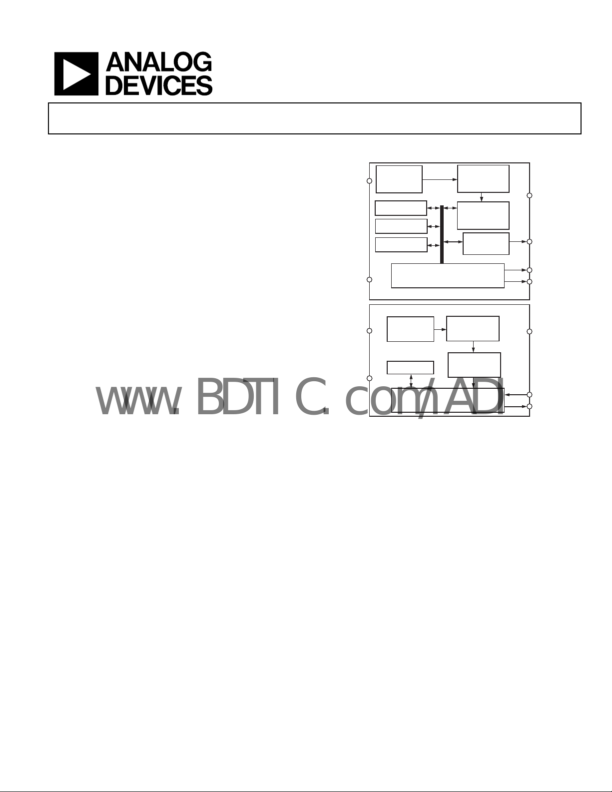
Temperature Sensors in SOT-23
AD7414/AD7415
FUNCTIONAL BLOCK DIAGRAM
GND
AS
GND
AS
SENSOR
CONFIGURATION
REGISTER
T
SETPOINT
HIGH
REGISTER
T
SETPOINT
LOW
REGISTER
AD7414
AD7415
BAND GAP
TEMPERATURE
SENSOR
CONFIGURATION
REGISTER
SMBus/I2C
INTERFACE
SMBus/I2C
INTERFACE
Figure 1.
BAND GAP
TEMPERATURE
limit is exceeded. A configuration register allows programming of
the state of the ALERT output (active high or active low). This
output can be used as an interrupt or as an SMBus alert.
PRODUCT HIGHLIGHTS
1. On-chip temperature sensor. The sensor allows an accurate
measurement of the ambient temperature to be made. It is
capable of ±0.5°C temperature accuracy.
2
2. SMBus/I
selectable choice of three addresses per version of the
AD7414/AD7415, eight address options in total for the AD7414,
and six in total for the AD7415.
3. Supply voltage of 2.7 V to 5.5 V.
4. Space-saving 5-lead and 6-lead SOT-23 packages.
5. 10-bit temperature reading to 0.25°C resolution.
6. Overtemperature indicator. This indicator can be software
disabled. It is used as an interrupt of SMBus alert.
7. One-shot and automatic temperature conversion rates.
One Technology Way, P.O. Box 9106, Norwood, MA 02062-9106, U.S.A.
Tel: 781.329.4700 www.analog.com
Fax: 781.461.3113 © 2005 Analog Devices, Inc. All rights reserved.
C-compatible serial interface. The interface offers pin
10-BIT
ANALOG-DIGITAL
CONVERTER
TEMPERATURE
VALUE
REGISTER
SETPOINT
COMPARATOR
10-BIT
ANALOG-DIGITAL
CONVERTER
TEMPERATURE
VALUE
REGISTER
V
ALERT
SCL
SDA
V
SCL
SDA
DD
DD
02463-001
Page 2

AD7414/AD7415
www.BDTIC.com/ADI
TABLE OF CONTENTS
Specifications .....................................................................................3
Absolute Maximum Ratings ............................................................5
ESD Caution ..................................................................................5
Pin Configurations and Function Descriptions............................6
Theory of Operation .........................................................................7
Circuit Information ......................................................................7
Functional Description.................................................................7
Measurement Technique..............................................................7
Temperature Data Format............................................................8
Internal Register Structure...............................................................9
Address Pointer Register..............................................................9
Configuration Register (Address 0X01).....................................9
Temperature Value Register (Address 0X00)...........................10
AD7414 T
AD7414 T
Register (Address 0X02)...................................10
HIGH
Register (Address 0X03) ....................................10
LOW
Serial Interface.................................................................................12
Serial Bus Address.......................................................................12
Writ e M o de ..................................................................................12
Read Mode...................................................................................12
SMBUS ALERT ............................................................................13
Power-On Defaults .....................................................................13
Operating Modes ........................................................................13
Power vs. Throughput ................................................................14
Mounting the AD7414/AD7415...............................................14
Supply Decoupling......................................................................14
Temperature Accuracy vs. Supply.............................................15
Typical Temperature Error Graph............................................15
Outline Dimensions........................................................................16
Ordering Guide...........................................................................17
REVISION HISTORY
4/05—Rev. D to Rev. E
Updated Format.................................................................. Universal
Changes to Absolute Maximum Ratings........................................6
Changes to Figure 6...........................................................................7
Changes to Ordering Guide...........................................................17
9/04—REV. C to REV. D.
C
hanges to ABSOLUTE MAXIMUM RATINGS.........................3
Updated ORDERING GUIDE.........................................................4
8/03—REV. B to REV. C.
Change to Temperature Range ......................................... Universal
Updated FEATURES.........................................................................1
Updated SPECIFICATIONS............................................................2
Updated ABSOLUTE MAXIMUM RATINGS.............................3
Updated ORDERING GUIDE.........................................................4
Updated CIRCUIT INFORMATION ............................................5
Updated TEMPERATURE DATA FORMAT................................6
Updated TEMPERATURE VALUE REGISTER ...........................8
Updated Figure 14...........................................................................11
Updated OUTLINE DIMENSIONS .............................................12
11/02—REV
Changes to ABSOLUTE MAXIMUM RATINGS......................... 3
10/02—REV. 0 to REV. A.
Changes to SPECIFICATIONS .......................................................2
Changes to PIN FUNCTION DESCRIPTIONS........................... 3
Changes to ABSOLUTE MAXIMUM RATINGS......................... 3
ORDERING GUIDE updated......................................................... 4
Change to Figure 2............................................................................ 5
Added to TYPICAL TEMPERATURE
ERROR GRAPH section ................................................................11
Added Figure 15..............................................................................11
OUTLINE DIMENSIONS updated..............................................12
7/01—Revision 0: Initial Version
. A to REV. B.
Rev. E | Page 2 of 20
Page 3
AD7414/AD7415
www.BDTIC.com/ADI
SPECIFICATIONS
TA = T
Table 1.
Parameter A Version Unit Test Conditions/Comments
TEMPERATURE SENSOR AND ADC
POWER SUPPLIES
DIGITAL INPUT
DIGITAL OUTPUT (OPEN-DRAIN)
AC ELECTRICAL CHARACTERISTICS
MIN
Accuracy
to T
, VDD = 2.7 V to 5.5 V, unless otherwise noted. Temperature range as follows: A version = −40°C to +125°C.
MAX
1
±0.5 °C typ VDD = 3 V @ +40°C
−0.87 to +0.822°C max VDD = 3 V @ +40°C
±1.5 °C max VDD = 3 V @ −40°C to +70°C
±2.0 °C max VDD = 3 V @ −40°C to +85°C
±3.0 °C max VDD = 3 V @ −40°C to +125°C
±2.0 °C typ VDD = 3 V @ −40°C to +125°C
±1.872 °C max VDD = 5.5 V @ +40°C
±2.0 °C typ VDD = 5.5 V @ −40°C to +85°C
±3.0 °C max VDD = 5.5 V @ −40°C to +85°C
±3.0 °C typ VDD = 5.5 V @ −40°C to +125°C
Resolution 10 Bits
Update Rate, t
R
800 ms typ
Temperature Conversion Time 25 µs typ
Supply Current
Peak Supply Current
3
4
1.2 mA typ Current during conversion
Supply Current – Nonconverting 900 µA max Peak current between conversions
Inactive Serial Bus
Normal Mode @ 3 V 169 µA typ
Normal Mode @ 5 V 188 µA typ
Active Serial Bus
Normal Mode @ 3 V 180 µA typ
Normal Mode @ 5 V 214 µA typ
Shutdown Mode 3 µA max
5
Supply current with serial bus inactive. Part not
converting and D7 of configuration register = 0.
6
Supply current with serial bus active. Part not
converting and D7 of configuration register = 0.
D7 of configuration register = 1. Typical values
are 0.04 µA at 3 V and 0.5 µA at 5 V.
Input High Voltage, V
Input Low Voltage, V
Input Current, I
Input Capacitance, C
Output High Voltage, V
Output Low Voltage, V
Output High Current, I
Output Capacitance, C
IH
IL
7
IN
IN
OH
OL
OH
OUT
ALERT Output Saturation Voltage 0.8 V max I
8, 9
Serial Clock Period, t
Data In Setup Time to SCL High, t
Data Out Stable after SCL Low, t
1
2
3
2.4 V min
0.8 V max
±1 µA max VIN = 0 V to V
DD
10 pF max All digital inputs
2.4 V min
0.4 V max IOL = 1.6 mA
1 µA max VOH = 5 V
10 pF max Typ = 3 pF
= 4 mA
OUT
2.5 µs min See Figure 2
50 ns min See Figure 2
0 ns min See Figure 2
Rev. E | Page 3 of 20
Page 4

AD7414/AD7415
www.BDTIC.com/ADI
Parameter A Version Unit Test Conditions/Comments
SDA Low Setup Time to SCL Low
(Start Condition), t
4
SDA High Hold Time after SCL High
(Stop Condition), t
SDA and SCL Fall Time, t
5
6
Power-Up Time 4 µs typ
1
Accuracy specifications apply only to voltages listed under Test Conditions. See Temperature Accuracy vs. Supply section for typical accuracy performance over the
full VDD supply range.
2
100% production tested at 40°C to these limits.
3
These current values can be used to determine average power consumption at different one-shot conversion rates. Average power consumption at the automatic
conversion rate of 1.25 kHz is 940 µW.
4
This peak supply current is required for 29 µs (the conversion time plus power-up time) out of every 800 µs (the conversion rate).
5
These current values are derived by not issuing a stop condition at the end of a write or read, thus preventing the part from going into a conversion.
6
The current is derived assuming a 400 kHz serial clock being active continuously.
7
On power-up, the initial input current, IIN, on the AS pin is typically 50 µA.
8
The SDA and SCL timing is measured with the input filters turned on so as to meet the fast mode I2C specification. Switching off the input filters improves the transfer
rate but has a negative effect on the EMC behavior of the part.
9
Guaranteed by design. Not tested in production.
50 ns min See Figure 2
50 ns min See Figure 2
90 ns max See Figure 2
t
SCL
SDA
DATA IN
SDA
DATA OUT
t
4
1
t
2
t
3
t
5
t
6
02463-002
Figure 2. Diagram for Serial Bus Timing
Rev. E | Page 4 of 20
Page 5

AD7414/AD7415
www.BDTIC.com/ADI
ABSOLUTE MAXIMUM RATINGS
Table 2.
Parameter Rating
VDD to GND −0.3 V to +7 V
SDA Input Voltage to GND −0.3 V to +7 V
SDA Output Voltage to GND −0.3 V to +7 V
SCL Input Voltage to GND −0.3 V to +7 V
ALERT Output Voltage to GND −0.3 V to +7 V
Operating Temperature Range −40°C to +125°C
Storage Temperature Range −65°C to +150°C
Junction Temperature 150°C
5-Lead SOT-23 (RJ-5)
Power Dissipation
Thermal Impedance
θJA, Junction-to-Ambient
1, 2
3
W
= (T
JMAX
− TA)/θ
JA
MAX
240°C/W
(still air)
6-Lead SOT-23 (RJ-6)
Power Dissipation
1, 2
W
= (T
JMAX
− TA)/θ
JA
MAX
Thermal Impedance3
θJA, Junction-to-Ambient
190.4°C/W
(still air)
8-Lead MSOP (RM-8)
Power Dissipation
1, 2
W
= (T
JMAX
− TA)/θ
JA
MAX
Thermal Impedance3
θJA, Junction-to-Ambient
205.9°C/W
(still air)
θJC, Junction-to-Case 43.74°C/W
IR Reflow Soldering
Peak Temperature 220°C (0°C/5°C)
Time at Peak Temperature 10 sec to 20 sec
Ramp-up Rate 3°C/s max
Ramp-down Rate
Ramp from 25°C to Peak
−6°C/s max
6 minutes max
Temperature
IR Reflow Soldering in Pb-Free
Package
Peak Temperature 260°C (0°C)
Time at Peak Temperature 20 sec to 40 sec
Ramp Rate 3°C/s max
Ramp-Down Rate
Ramp from 25°C to Peak
−6°C/s max
8 minutes max
Temperature
1
Values relate to package being used on a standard 2-layer PCB.
2
TA = ambient temperature.
3
Junction-to-case resistance is applicable to components featuring a
preferential flow direction, such as components mounted on a heat sink.
Junction-to-ambient resistance is more useful for air-cooled, PCB-mounted
components.
Stresses above those listed under Absolute Maximum Ratings
may cause permanent damage to the device. This is a stress
rating only; functional operation of the device at these or any
other conditions above those indicated in the operational
section of this specification is not implied. Exposure to absolute
maximum rating conditions for extended periods may affect
device reliability.
ESD CAUTION
ESD (electrostatic discharge) sensitive device. Electrostatic charges as high as 4000 V readily accumulate on the
human body and test equipment and can discharge without detection. Although this product features
proprietary ESD protection circuitry, permanent damage may occur on devices subjected to high energy
electrostatic discharges. Therefore, proper ESD precautions are recommended to avoid performance
degradation or loss of functionality
.
Rev. E | Page 5 of 20
Page 6
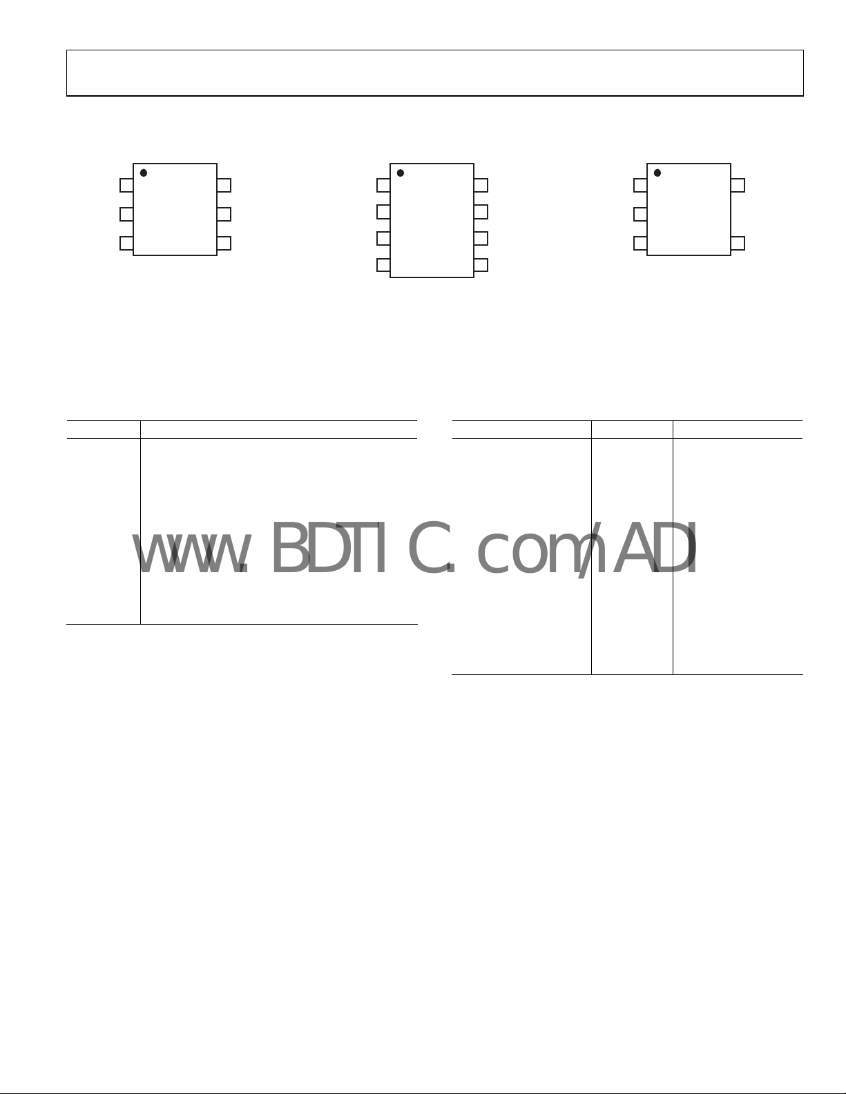
AD7414/AD7415
A
T
www.BDTIC.com/ADI
PIN CONFIGURATIONS AND FUNCTION DESCRIPTIONS
SDA
AS
GND 2
V
DD
1
3
AD7414
Top View
(Not to Scale)
6
5
4
ALERT
SCL
02463-003
Figure 3. AD7414 Pin Configuration (SOT-23)
Table 3. Pin Function Descriptions
Mnemonic Description
AS
Logic Input. Address select input that selects one
of three I2C addresses for the AD7414/AD7415 (see
Table 4). Recommend a pull-up or pull-down
resistor of 1 kΩ.
GND Analog and Digital Ground.
V
DD
SDA
Positive Supply Voltage, 2.7 V to 5.5 V.
Digital I/O. Serial bus bidirectional data. Open-
drain output.
ALERT
AD7414 Digital Output. Overtemperature
indicator becomes active when temperature
exceeds T
. Open-drain output.
HIGH
SCL Digital Input. Serial bus clock.
1
NC
AD7414
SDA 2
LER
SCL V
Top View
(Not to Scale)
3
4
NC = NO CONNECT
NC
8
AS
7
GND
6
5
DD
02463-004
Figure 4. AD7414 Pin Configuration (MSOP)
2
Table 4. I
C Address Selection
Part Number AS Pin I2C Address
AD7414-0 Float 1001 000
AD7414-0 GND 1001 001
AD7414-0 V
AD7414-1 Float 1001 100
AD7414-1 GND 1001 101
AD7414-1 V
AD7414-2 N/A 1001 011
AD7414-3 N/A 1001 111
AD7415-0 Float 1001 000
AD7415-0 GND 1001 001
AD7415-0 V
AD7415-1 Float 1001 100
AD7415-1 GND 1001 101
AD7415-1 V
SDA
AS
GND 2
V
DD
1
3
AD7415
Top View
(Not to Scale)
5
SCL
4
02463-005
Figure 5. AD7415 Pin Configuration (SOT-23)
DD
DD
DD
DD
1001 010
1001 110
1001 010
1001 110
Rev. E | Page 6 of 20
Page 7

AD7414/AD7415
(
×=∆
www.BDTIC.com/ADI
THEORY OF OPERATION
CIRCUIT INFORMATION
The AD7414/AD7415 are standalone digital temperature
sensors. The on-chip temperature sensor allows an accurate
measurement of the ambient device temperature to be made.
The 10-bit analog-to-digital converter converts the temperature
measured into a twos complement format for storage in the
temperature register. The ADC is made up of a conventional
successive-approximation converter based around a capacitor
digital-to-analog (DAC). The serial interface is I
2
C-and SMBuscompatible. The AD7414/AD7415 require a 2.7 V to 5.5 V
power supply. The temperature sensor has a working
measurement range of −40°C to +125°C.
FUNCTIONAL DESCRIPTION
Temperature measurement is initiated by two methods. The
first uses an internal clock countdown of 800 ms, and a
conversion is performed. The internal oscillator is the only
circuit that is powered up between conversions, and once it
times out, every 800 ms, a wake-up signal is sent to power up
the rest of the circuitry. A monostable is activated at the
beginning of the wake-up signal to ensure that sufficient time is
given to the power-up process. The monostable typically takes
4 µs to time out. It then takes typically 25 µs for each conversion
to be completed. The new temperature value is loaded into the
temperature value register and ready for reading by the I
interface.
A temperature measurement is also initiated every time the
one-shot method is used. This method requires the user to
write to the one-shot bit in the configuration register when a
temperature measurement is needed. Setting the one-shot bit to
1 starts a temperature conversion directly after the write
operation. The track-and-hold goes into hold approximately
4 µs (monostable time out) after the STOP condition, and a
conversion is then initiated. Typically 25 µs later, the conversion
is complete and the temperature value register is loaded with a
new temperature value.
The measurement modes are compared with a high temperature limit, stored in an 8-bit read/write register. This is applicable only to the AD7414, because the AD7415 does not have an
ALERT pin and subsequently does not have an overtemperature
monitoring function. If the measurement is greater than the
high limit, the ALERT pin is activated (if it has already been
enabled in the configuration register). There are two ways to
deactivate the ALERT pin again: when the alert reset bit in the
configuration register is set to 1 by a write operation, and when
the temperature measured is less than the value in the T
register. This ALERT pin is compatible with the SMBus
SMBALERT option.
2
LOW
C
Configuration functions consist of
• Switching between normal operation and full power-
down
• Enabling or disabling the SCL and SDA filters
• Enabling or disabling the ALERT function
• Setting the ALERT pin polarity
SUPPLY
2.7V TO
5.5V
10µF 1kΩ0.1µF
VDDVDDV
10kΩ 10kΩ 10kΩ
V
DD
AS
GND
Figure 6. Typical Connection Diagram
SDA
SCL
ALERT
AD7414
DD
µC/µ
P
MEASUREMENT TECHNIQUE
A common method of measuring temperature is to exploit the
negative temperature coefficient of a diode, or the base-emitter
voltage of a transistor, operated at constant current.
Unfortunately, this technique requires calibration to null the
effect of the absolute value of V
device. The technique used in the AD7414/AD7415 is to
measure the change in V
BE
different currents. This is given by
BE
NlnqKTV
where:
K is Boltzmann’s constant.
q is the charge on the electron (1.6 × 10
T is the absolute temperature in Kelvins.
N is the ratio of the two currents.
, which varies from device to
BE
when the device is operated at two
)
–19
Coulombs).
02463-006
Rev. E | Page 7 of 20
Page 8

AD7414/AD7415
−
www.BDTIC.com/ADI
SENSING
TRANSISTOR
II× N
SENSING
TRANSISTOR
Figure 7. Temperature Measurement Technique
V
DD
V
+
OUT
TO ADC
–
V
OUT
02463-007
Figure 7 shows the method the AD7414/AD7415 use to
measure the ambient device temperature. To measure ΔV
,
BE
the sensor (substrate transistor) is switched between operating
currents of I and N × I. The resulting waveform is passed
through a chopper stabilized amplifier that performs the
functions of amplification and rectification of the waveform to
produce a dc voltage proportional to ΔV
. This voltage is
BE
measured by the ADC to give a temperature output in 10-bit,
twos complement format.
TEMPERATURE DATA FORMAT
The temperature resolution of the ADC is 0.25°C, which
corresponds to 1 LSB of the ADC. The ADC can theoretically
measure a temperature span of 255°C; the lowest practical value
is limited to −40°C due to the device maximum ratings. The
A grade can measure a temperature range of −40°C to +125°C.
(Temperature data format is shown in Table 5.)
Table 5. A Grade Temperature Data Format
Temperature Digital Output DB9…DB0
−55°C 11 0010 0100
−50°C 11 0011 1000
−25°C 11 1001 1100
−0.25°C 11 1111 1111
0°C 00 0000 0000
+0.25°C 00 0000 0001
+10°C 00 0010 1000
+25°C 00 0110 0100
+50°C 00 1100 1000
+75°C 01 0010 1100
+100°C 01 1001 0000
+125°C 01 1111 0100
The grade temperature conversion formula follows:
eTemperaturPositive =
=
eTemperaturNegative
)(dCodeADC
4
dCodeADC
512)(
4
Note that DB9 is removed from the ADC code in the negative
temperature formula.
Rev. E | Page 8 of 20
Page 9

AD7414/AD7415
www.BDTIC.com/ADI
INTERNAL REGISTER STRUCTURE
The AD7414 has five internal registers, as shown in Figure 8.
Four are data registers, and one is an address pointer register.
TEMPERATURE
VALUE
REGISTER
CONFIGURATION
ADDRESS
POINTER
REGISTER
REGISTER
T
HIGH
REGISTER
T
LOW
REGISTER
SERIAL BUS INTERFACE
Figure 8. AD7414 Register Structure
D
A
T
A
SDA
SCL
The AD7415 has three internal registers, as shown in Figure 9.
Two are data registers, and one is an address pointer register.
02463-008
Table 6. Address Pointer Register
P7 P6 P5 P4 P3 P2 P1 P0
0 0 0 0 0 0 Register Select
Table 7. AD7414 Register Address
P1 P0 Register
0 0 Temperature value register (read-only)
0 1 Configuration register (read/write)
1 0 T
1 1 T
register (read/write)
HIGH
register (read/write)
LOW
Table 8. AD7415 Register Address
P1 P0 Registers
0 0 Temperature value register (read-only)
0 1 Configuration register (read/write)
Table 9. AD7414 Configuration Register
D7 D6 D5 D4 D3 D2 D1 D0
PD FLTR
ALERT
EN
1
011
1
Default settings at power-up.
1
0
ALERT
POLARITY
1
0
ALERT
RESET
1
0
ONE
SHOT
1
0
TEST
MODE
1
0s
TEMPERATURE
VALUE
ADDRESS
POINTER
REGISTER
Figure 9. AD7415 Register Structure
REGISTER
CONFIGURATION
REGISTER
D
A
T
A
SDA
SCL
02463-009
Each data register has an address pointed to by the address
pointer register when communicating with it. The temperature
value register is the only data register that is read-only.
ADDRESS POINTER REGISTER
The address pointer register is an 8-bit register that stores an
address that points to one of the four data registers of the
AD7414 and one of the two data registers of the AD7415. The
first byte of every serial write operation to the AD7414/AD7415
is the address of one of the data registers, which is stored in the
address pointer register and selects the data register to which
subsequent data bytes are written. Only the 2 LSBs of this
register are used to select a data register.
CONFIGURATION REGISTER (ADDRESS 0X01)
The configuration register is an 8-bit read/write register that is
used to set the operating modes of the AD7414/AD7415. In the
AD7414, six of the MSBs are used (D7 to D2) to set the
operating modes (see Table 10). D0 and D1 are used for factory
settings and must have zeros written to them during normal
operation.
Table 10. AD7414 Configuration Register Settings
D7 Full power-down if = 1.
D6 Bypass SDA and SCL filtering if = 0.
D5 Disable ALERT if = 1.
D4 ALERT is active low if D4 = 0, ALERT is active high if D4 = 1.
D3
Reset the ALERT pin if set to 1. The next temperature
conversion has the ability to activate the ALERT function.
The bit status is not stored; thus this bit is 0 if read.
D2
Initiate a one shot temperature conversion if set to a 1.
The bit status is not stored; thus this bit is 0 if read.
Table 11. AD7415 Configuration Register
D7 D6 D5 D4 D3 D2 D1 D0
PD FLTR ONE SHOT TEST MODE
1
011
1
Default settings at power-up.
TEST MODE
0s1 0s
1
0s1
Rev. E | Page 9 of 20
Page 10

AD7414/AD7415
www.BDTIC.com/ADI
In the AD7415, only three of the bits are used (D7, D6, and D2)
to set the operating modes (see Table 12). D0, D1, and D3 to D5
are used for factory settings and must have zeros written to
them during normal operation.
Table 12. AD7415 Configuration Register Settings
D7 Full power-down if = 1.
D6 Bypass SDA and SCL filtering if = 0.
D2 Initiate a one-shot temperature conversion if set to 1.
The bit status is not stored; thus this bit is 0 if read.
If the AD7414/AD7415 are in power-down mode (D7 = 1), a
temperature conversion can still be initiated by the one-shot
operation. This involves a write operation to the configuration
register and setting the one-shot bit to 1 (D2 = 1), which causes
the AD7414/AD7415 to power up, perform a single conversion,
and power down again. This is a very power efficient mode.
TEMPERATURE VALUE REGISTER (ADDRESS 0X00)
The temperature value register is a 10-bit, read-only register
that stores the temperature reading from the ADC in twos
complement format. Two reads are necessary to read data from
this register. Table 13 shows the contents of the first byte to be
read, while Table 14 and Table 15 show the contents of the
second byte to be read from the AD7414 and AD7415,
respectively. In Table 14, D3 to D5 of the second byte are used
as flag bits and are obtained from other internal registers. They
function as follows:
ALERT_Flag: The state of this bit is the same as that of the
ALER
T pin.
_Flag: This flag is set to 1 when the temperature
T
HIGH
measured goes above the T
when the second temperature byte (Table 14) is
read. If the temperature is still greater than the
T
limit after the read operation, the flag is
HIGH
again.
_Flag: This flag is set to 1 when the temperature
T
LOW
measured goes below the T
when the second temperature byte (Table 14) is
read. If the temperature is still less than the T
limit after the read operation, the flag is set again.
limit. It is reset
HIGH
limit. It is reset
LOW
LOW
Table 13. Temperature Value Register (First Read)
D15 D14 D13 D12 D11 D10 D9 D8
MSB B8 B7 B6 B5 B4 B3 B2
Table 14. AD7414 Temperature Value Register (Second Read)
D7 D6 D5 D4 D3 D2 D1 D0
B1 LSB ALERT_Flag T
_Flag T
HIGH
_Flag 0 0 0
LOW
Table 15. AD7415 Temperature Value Register (Second Read)
D7 D6 D5 D4 D3 D2 D1 D0
B1 LSB N/A N/A N/A N/A N/A N/A
AD7414 T
The T
HIGH
REGISTER (ADDRESS 0X02)
HIGH
register (see Table 16) is an 8-bit, read/write register
that stores the upper limit that activates the ALERT output.
Therefore, if the value in the temperature value register is
greater than the value in the T
register, the ALERT pin is
HIGH
activated (that is, if ALERT is enabled in the configuration
register). Because it is an 8-bit register, the temperature
resolution is 1°C.
Table 16. T
D7 D6 D5 D4 D3 D2 D1 D0
MSB B6 B5 B4 B3 B2 B1 B0
HIGH
Register
AD7414 T
The T
LOW
REGISTER (ADDRESS 0X03)
LOW
register (see Table 17) is an 8-bit read/write register
that stores the lower limit that deactivates the ALERT output.
Therefore, if the value in the temperature value register is less
than the value in the T
register, the ALERT pin is
LOW
deactivated (that is, if ALERT is enabled in the configuration
register).
Because it is an 8-bit register, the temperature resolution is 1°C.
Table 17. T
D7 D6 D5 D4 D3 D2 D1 D0
MSB B6 B5 B4 B3 B2 B1 B0
Register
LOW
The full theoretical span of the ADC is 255°C, but in practice
he temperature measurement range is limited to the operating
t
range of the device, −40°C to +125°C for the A grade.
Rev. E | Page 10 of 20
Page 11

AD7414/AD7415
SDA
Y
www.BDTIC.com/ADI
SCL
START BY
MASTER
9
1
1
0
0
SERIAL BUS ADDRESS BYTE
A2
1
FRAME 1
A0
A1
R/W
ACK. BY
AD7414/AD7415
1
P6
P7
P5
ADDRESS POINTER REGISTER BYTE
P4
P3
FRAME 2
P1
P2
9
P0
ACK. BY
AD7414/AD7415
STOP BY
MASTER
02463-010
Figure 10. Writing to the Address Pointer Register to Select a Register for a Subsequent Read Operation
9
ACK. BY
AD7414/AD7415
91
STOP BY
MASTER
•••
•••
02463-011
SCL
SDA
START B
MASTER
1
11
SERIAL BUS ADDRESS BYTE
A2
1
FRAME 1
SDA (CONTINUED)
A0
A1
SCL (CONTINUED)
R/W
ACK. BY
AD7414/AD7415
•••
•••
D7
P7
D6
191
P6
P5
ADDRESS POINTER REGISTER BYTE
D5
D4
DATA BYTE
P4
D3
FRAME 3
P3
FRAME 2
D2
P1 P0
P2
D1
D0
ACK. BY
AD7414/AD7415
Figure 11. Writing to the Address Pointer Register Followed by a Single Byte of Data to the Selected Register
SCL
SDA
START BY
MASTER
0
1
SERIAL BUS ADDRESS BYTE
R/W
AD7414/AD7415
FRAME 1
ACK. BY
D7 D6 D5 D4 D3 D2 D1 D0A0A1A210
SINGLE DATA BYTE FROM AD7414/AD7415
FRAME 2
NO ACK. BY
MASTER
STOPBY
MASTER
02463-012
Figure 12. Reading a Single Byte of Data from a Selected Register
SCL
SDA
START BY
MASTER
1
1
0
0
FRAME 1
SERIAL BUS ADDRESS BYTE
SDA (CONTINUED)
SCL (CONTINUED)
A2
1
A0
A1
9
R/W
ACK. BY
AD7414/AD7415
1
•••
•••
D7
LEAST SIGNIFICANT DATA BYTE FROM AD7414/AD7415
1
D14
D15
MOST SIGNIFICANT DATA BYTE FROM AD7414/AD7415
D6
D5
D13
D4
D12
D3
FRAME 3
D10
FRAME 2
D2
D11
D1
D9 D8
D0
NO ACK. BY
MASTER
MASTER
9
9
ACK. BY
STOP BY
MASTER
•••
•••
02463-013
Figure 13. Reading Two Bytes of Data from the Temperature Value Register
Rev. E | Page 11 of 20
Page 12

AD7414/AD7415
www.BDTIC.com/ADI
SERIAL INTERFACE
Control of the AD7414/AD7415 is carried out via the I2Ccompatible serial bus. The AD7414/AD7415 are connected to
this bus as slave device, under the control of a master device,
such as the processor.
SERIAL BUS ADDRESS
Like all I2C-compatible devices, the AD7414/AD7415 have a
7-bit serial address. The four MSBs of this address for the
AD7414/AD7415 are set to 1001. The AD7414/AD7415 are
available in four versions: AD7414/AD7415-0, AD7414/
AD7415-1, AD7414-2, and AD7414-3. The first two versions
have three different I
by either tying the AS pin to GND, to V
float (see Table 4). By giving different addresses for the four
versions, up to eight AD7414s or six AD7415s can be connected
to a single serial bus, or the addresses can be set to avoid
conflicts with other devices on the bus.
The serial bus protocol operates as follows.
The master initiates data transfer by establishing a START
co
ndition, defined as a high-to-low transition on the serial data
line SDA, while the serial clock line SCL remains high. This
indicates that an address/data stream follows. All slave peripherals connected to the serial bus respond to the START condition and shift in the next eight bits, consisting of a 7-bit address
(MSB first) plus an R/
the data transfer and whether data is written to or read from the
slave device.
The peripheral whose address corresponds to the transmitted
addr
ess responds by pulling the data line low during the low
period before the ninth clock pulse, known as the acknowledge
bit. All other devices on the bus remain idle while the selected
device waits for data to be read from or written to it. If the R/
bit is 0, the master writes to the slave device. If the R/
the master reads from the slave device.
Data is sent over the serial bus in sequences of nine clock
ulses, eight bits of data followed by an acknowledge bit from
p
the receiver of data. Transitions on the data line must occur
during the low period of the clock signal and remain stable
during the high period, because a low-to-high transition when
the clock is high may be interpreted as a STOP signal.
When all data bytes have been read or written, stop conditions
a
re established. In WRITE mode, the master pulls the data line
high during the 10th clock pulse to assert a STOP condition. In
READ mode, the master device pulls the data line high during
the low period before the ninth clock pulse. This is known as
No Acknowledge. The master then takes the data line low
during the low period before the 10th clock pulse, then high
during the 10th clock pulse to assert a STOP condition.
2
C addresses available, which are selected
, or letting the pin
DD
bit, which determines the direction of
W
bit is 1,
W
W
Any number of bytes of data may be transferred over the serial
b
us in one operation, but it is not possible to mix read and write
in one operation. The type of operation is determined at the
beginning and cannot then be changed without starting a new
operation.
WRITE MODE
Depending on the register being written to, there are two
different writes for the AD7414/AD7415.
Writing to the Address Pointer Register for a Subsequent
Read
In order to read data from a particular register, the address
pointer register must contain the address of that register. If it
does not, the correct address must be written to the address
pointer register by performing a single-byte write operation, as
shown in Figure 10. The write operation consists of the serial
bus address followed by the address pointer byte. No data is
written to any of the data registers. A read operation is then
performed to read the register.
Writing a Single Byte of Data to the Configuration
Register,T
All three registers are 8-bit registers, so only one byte of data
can be written to each register. Writing a single byte of data to
one of these registers consists of the serial bus address, the data
register address written to the address pointer register, followed
by the data byte written to the selected data register. This is
illustrated in Figure 11.
Register, or T
HIGH
Register
LOW
READ MODE
Reading data from the AD7414/AD7415 is a 1- or 2-byte
operation. Reading back the contents of the configuration
register, the T
read operation, as shown in Figure 12. The register address was
previously set up by a single-byte write operation to the address
pointer register. Once the register address has been set up, any
number of reads can subsequently be performed from that
register without having to write to the address pointer register
again. To read from another register, the address pointer
register has to be written to again to set up the relevant register
address.
Reading data from the temperature value register is a 2-byte
o
peration, as shown in Figure 13. The same rules apply for a
2-byte read as a 1-byte read.
register, or the T
HIGH
register is a single-byte
LOW
Rev. E | Page 12 of 20
Page 13

AD7414/AD7415
www.BDTIC.com/ADI
SMBUS ALERT
The AD7414 ALERT output is an SMBus interrupt line for
devices that want to trade their ability to master for an extra
pin. The AD7414 is a slave-only device and uses the SMBus
ALERT to signal to the host device that it wants to talk. The
SMBus ALERT on the AD7414 is used as an overtemperature
indicator.
The ALERT pin has an open-drain configuration that allows the
ALER
T outputs of several AD7414s to be wire-AND’ed together
when the ALERT pin is active low. Use D4 of the configuration
register to set the active polarity of the ALERT output. The
power-up default is active low. The ALERT function can be
disabled or enabled by setting D5 of the configuration register
to 1 or 0, respectively.
The host device can process the ALERT interrupt and
sim
ultaneously access all SMBus ALERT devices through the
alert response address. Only the device that pulled the ALERT
low acknowledges the Alert Response Address (ARA). If more
than one device pulls the ALERT pin low, the highest priority
(lowest address) device wins communication rights via standard
2
I
C arbitration during the slave address transfer.
The ALERT output becomes active when the value in the
emperature value register exceeds the value in the T
t
register. It is reset when a write operation to the configuration
register sets D3 to 1 or when the temperature falls below the
value stored in the T
The ALERT output requires an external pull-up resistor. This
n be connected to a voltage different from V
ca
maximum voltage rating of the ALERT output pin is not
exceeded. The value of the pull-up resistor depends on the
application, but it should be as large as possible to avoid
excessive sink currents at the ALERT output, which can heat the
chip and affect the temperature reading.
register.
LOW
DD
HIGH
, provided the
POWER-ON DEFAULTS
The AD7414/AD7415 always power up with these defaults:
Address pointer register pointing to the temperature value
gister.
re
OPERATING MODES
Mode 1
This is the power-on default mode of the AD7414/AD7415. In
this mode, the AD7414/AD7415 does a temperature conversion
every 800 ms and then partially powers down until the next
conversion occurs.
If a one-shot operation (setting D2 of the configuration register
t
o a 1) is performed between automatic conversions, a conversion is initiated right after the write operation. After this
conversion, the part returns to performing a conversion every
800 ms.
Depending on where a serial port access occurs during a
co
nversion, that conversion might be aborted. If the conversion
is completed before the part recognizes a serial port access, the
temperature register is updated with the new conversion. If the
conversion is completed after the part recognizes a serial port
access, the internal logic prevents the temperature register from
being updated, because corrupt data could be read.
A temperature conversion can start anytime during a serial port
acces
s (other than a one-shot operation), but the result of that
conversion is loaded into the temperature register only if the
serial port access is not active at the end of the conversion.
Mode 2
The only other mode in which the AD7414/AD7415 operates is
the full power-down mode. This mode is usually used when
temperature measurements are required at a very slow rate. The
power consumption of the part can be greatly reduced in this
mode by writing to the part to go to a full power-down. Full
power-down is initiated right after D7 of the configuration
register is set to 1.
When a temperature measurement is required, a write
o
peration can be performed to power up the part and put it into
one-shot mode (setting D2 of the configuration register to a 1).
The power-up takes approximately 4
a conversion and is returned to full power-down. The
temperature value can be read in the full power-down mode,
because the serial interface is still powered up.
µs. The part then performs
register loaded with 7Fh.
T
HIGH
register loaded with 80h.
T
LOW
Configuration register loaded with 40h.
Note that the AD7415 does not have any T
HIGH
or T
registers.
LOW
Rev. E | Page 13 of 20
Page 14

AD7414/AD7415
www.BDTIC.com/ADI
POWER VS. THROUGHPUT
The two modes of operation for the AD7414/AD7415 produce
different power vs. throughput performances. Mode 2 is the
sleep mode of the part, and it achieves the optimum power
performance.
Mode 1
In this mode, continuous conversions are performed at a rate of
approximately one every 800 ms. Figure 14 shows the times and
currents involved with this mode of operation for a 5 V supply.
At 5 V, the current consumption for the part when converting is
1.1 mA typically, and the quiescent current is 188 µA typically.
The conversion time of 25 µs plus power-up time of typically
4 µs contributes 199.3 nW to the overall power dissipation in
the following way:
(29 µs/800 ms) × (5 × 1.1 mA) = 199.3 nW
The contribution to the total power dissipated by the remaining
time is 939.96 µW.
(799.97 ms/800 ms) × (5 × 1.1 µA) = 199.3 µW
Thus the total power dissipated during each cycle is
199.3 nW + 939.96 µW = 940.16 µW
1.1mA
I
DD
Figure 14. Mode 1 Power Dissipation
Mode 2
In this mode, the part is totally powered down. All circuitry
except the serial interface is switched off. The most power
efficient way of operating in this mode is to use the one-shot
method. Write to the configuration register and set the one-shot
bit to a 1. The part powers up in approximately 4
performs a conversion. Once the conversion is finished, the
device powers down again until the PD bit in the configuration
register is set to 0 or the one-shot bit is set to 1. Figure 15 shows
the same timing as Figure 14 in mode 1; a one-shot is initiated
every 800 ms. If we take the voltage supply to be 5 V, we can
work out the power dissipation in the following way. The
current consumption for the part when converting is 1.1 mA
typically, and the quiescent current is 800 nA typically. The
conversion time of 25 µs plus the power-up time of
800ms
188µA
29µs
TIME
µs and then
02463-014
typically 4
µs contributes 199.3 nW to the overall power
dissipation in the following way:
(29 µs/800 ms) × (5 V × 1.1 mA) = 199.3 nW
The contribution to the total power dissipated by the remaining
time is 3.9 µW.
(799.971 ms/800 ms) × (5 V × 800 nA) = 3.9 µW
Thus the total power dissipated during each cycle is:
199.3 nW + 3.9 µW = 940.16 µW
1.1mA
I
DD
Figure 15. Mode 2 Power Dissipation
800ms
800nA
29µs
TIME
MOUNTING THE AD7414/AD7415
The AD7414/AD7415 can be used for surface or air temperature sensing applications. If the device is cemented to a surface
with thermally conductive adhesive, the die temperature is
within about 0.1°C of the surface temperature, due to the
device’s low power consumption. Care should be taken to
insulate the back and leads of the device from the air if the
ambient air temperature is different from the surface
temperature being measured.
The ground pin provides the best thermal path to the die, so the
temperature of the die is close to that of the printed circuit
ground track. Care should be taken to ensure that this is in
good thermal contact with the surface being measured.
As with any IC, the AD7414/AD7415 and their associated
wiring and circuits must be kept free from moisture to prevent
leakage and corrosion, particularly in cold conditions where
condensation is more likely to occur. Water-resistant varnishes
and conformal coatings can be used for protection. The small
size of the AD7414/AD7415 packages allows them to be
mounted inside sealed metal probes, which provide a safe
environment for the devices.
SUPPLY DECOUPLING
The AD7414/AD7415 should at least be decoupled with a 0.1µF
ceramic capacitor between V
important if the AD7414/AD7415 are mounted remote from
the power supply.
and GND. This is particularly
DD
02463-015
Rev. E | Page 14 of 20
Page 15

AD7414/AD7415
www.BDTIC.com/ADI
TEMPERATURE ACCURACY VS. SUPPLY
The temperature accuracy specifications are guaranteed for
voltage supplies of 3 V and 5.5 V only. Figure 16 gives the
typical performance characteristics of a large sample of parts
over the full voltage range of 2.7 V to 5.5 V. Figure 17 gives the
typical performance characteristics of one part over the full
voltage range of 2.7 V to 5.5 V.
4
3
2
1
0
–1
–2
TEMPERATURE ERROR (°C)
–3
–40°C
+40°C
+85°C
TYPICAL TEMPERATURE ERROR GRAPH
Figure 18 shows the typical temperature error plots for one
device with V
4
3
2
1
0
–1
–2
TEMPERATURE ERROR (°C)
–3
–4
–40–30 –20 –10 0 10 20 30 40 50 60 70 80 90 95 100 110 125
at 3.3 V and at 5.5 V.
DD
5.5V
3.3V
TEMPERATURE (°C)
Figure 18. Typical Temperature Error @ 3.3 V and 5.5 V
02463-018
–4
2.7
3.0
SUPPLYVOLTAGE (V)
5.5
Figure 16. Typical Temperature Error vs. Supply for Large Sample of Parts
4
3
2
1
0
–1
–2
TEMPERATURE ERROR (°C)
–3
–4
2.7
+40°C
3.3 5.0
SUPPLYVOLTAGE (V)
–40°C
+85°C
5.5
Figure 17. Typical Temperature Error vs. Supply for One Part
02463-016
02463-017
Figure 19 shows a histogram of the temperature error at
ambient temperature (40°C) over approximately 6,000 units.
Figure 19 shows that over 70% of the AD7414/AD7415 devices
tested have a temperature error within ±0.3°C.
900
AMBIENT TEMPERATURE = 40°C
800
700
600
500
400
300
NUMBER OF UNITS
200
100
0
–1.08 –0.81 –0.54 –0.27 0 0.27 0.54 0.81 1.08
Figure 19. Ambient Temperature Error @ 3 V
TEMPERATURE ERROR (°C)
02463-019
Rev. E | Page 15 of 20
Page 16

AD7414/AD7415
www.BDTIC.com/ADI
OUTLINE DIMENSIONS
2.90 BSC
6
1.60 BSC
1 3452
PIN 1
INDICATOR
1.30
1.15
0.90
0.15MAX
1.90
BSC
0.50
0.30
COMPLIANT TO JEDEC STANDARDS MO-178AB
Figure 20. 6-Lead Small Outline Transistor Package [SOT-23]
Dimensions shown in millimeters
2.80 BSC
0.95 BSC
1.45 MAX
SEATING
PLANE
(RT-6)
0.22
0.08
10°
3.00
BSC
8
5
3.00
BSC
1
PIN 1
0.65 BSC
0.15
0.60
4°
0.45
0°
0.30
0.00
0.38
0.22
COPLANARITY
0.10
COMPLIANT TO JEDEC STANDARDS MO-187-AA
Figure 21. 8-Lead Mini Small Outline Package [MSOP]
4.90
BSC
4
1.10 MAX
8°
0°
SEATING
PLANE
0.23
0.08
(RM-8)
Dimensions shown in millimeters
0.80
0.60
0.40
2.90 BSC
4 5
0.50
0.30
3
2.80 BSC
0.95 BSC
1.45 MAX
SEATING
PLANE
0.22
0.08
10°
5°
0°
0.60
0.45
0.30
1.60 BSC
1.30
1.15
0.90
0.15MAX
1
2
PIN 1
1.90
BSC
COMPLIANT TO JEDEC STANDARDS MO-178AA
Figure 22. 5-Lead Small Outline Transistor Package [SOT-23]
(RT-5)
Dimensions shown in millimeters
Rev. E | Page 16 of 20
Page 17

AD7414/AD7415
www.BDTIC.com/ADI
ORDERING GUIDE
Temperature
Model
AD7414ART-0REEL7 −40°C to +125°C ±2°C RT-6 6-Lead SOT-23 CHA 3,000
AD7414ART-0REEL −40°C to +125°C ±2°C RT-6 6-Lead SOT-23 CHA 10,000
AD7414ART-0500RL7 −40°C to +125°C ±2°C RT-6 6-Lead SOT-23 CHA 500
AD7414ARTZ-0REEL7
AD7414ARTZ-0REEL1 −40°C to +125°C ±2°C RT-6 6-Lead SOT-23 #CHA 10,000
AD7414ARTZ-0500RL71 −40°C to +125°C ±2°C RT-6 6-Lead SOT-23 #CHA 500
AD7414ARM-0REEL7 −40°C to +125°C ±2°C RM-8 8-Lead MSOP CHA 3,000
AD7414ARM-0REEL −40°C to +125°C ±2°C RM-8 8-Lead MSOP CHA 10,000
AD7414ARM-0 −40°C to +125°C ±2°C RM-8 8-Lead MSOP CHA
AD7414ARMZ-0REEL71 −40°C to +125°C ±2°C RM-8 8-Lead MSOP TOL 3,000
AD7414ARMZ-0REEL1 −40°C to +125°C ±2°C RM-8 8-Lead MSOP TOL 10,000
AD7414ARMZ-01 −40°C to +125°C ±2°C RM-8 8-Lead MSOP TOL
AD7414ART-1REEL7 −40°C to +125°C ±2°C RT-6 6-Lead SOT-23 CHB 3,000
AD7414ART-1REEL −40°C to +125°C ±2°C RT-6 6-Lead SOT-23 CHB 10,000
AD7414ART-1500RL7 −40°C to +125°C ±2°C RT-6 6-Lead SOT-23 CHB 500
AD7414ARTZ-1REEL71 −40°C to +125°C ±2°C RT-6 6-Lead SOT-23 TOH 3,000
AD7414ARTZ-1REEL1 −40°C to +125°C ±2°C RT-6 6-Lead SOT-23 TOH 10,000
AD7414ARTZ-1500RL71 −40°C to +125°C ±2°C RT-6 6-Lead SOT-23 TOH 500
AD7414ARM-1REEL7 −40°C to +125°C ±2°C RM-8 8-Lead MSOP CHB 3,000
AD7414ARM-1REEL −40°C to +125°C ±2°C RM-8 8-Lead MSOP CHB 10,000
AD7414ARM-1 −40°C to +125°C ±2°C RM-8 8-Lead MSOP CHB
AD7414ARMZ-1REEL71 −40°C to +125°C ±2°C RM-8 8-Lead MSOP TOH 3,000
AD7414ARMZ-1REEL1 −40°C to +125°C ±2°C RM-8 8-Lead MSOP TOH 10,000
AD7414ARMZ-11 −40°C to +125°C ±2°C RM-8 8-Lead MSOP TOH
AD7414ART-2REEL7 −40°C to +125°C ±2°C RT-6 6-Lead SOT-23 CHC 3,000
AD7414ART-2REEL −40°C to +125°C ±2°C RT-6 6-Lead SOT-23 CHC 10,000
AD7414ARTZ-2REEL71 −40°C to +125°C ±2°C RT-6 6-Lead SOT-23 TOJ 3,000
AD7414ARTZ-2REEL1 −40°C to +125°C ±2°C RT-6 6-Lead SOT-23 TOJ 10,000
AD7414ART-3REEL7 −40°C to +125°C ±2°C RT-6 6-Lead SOT-23 CHD 3,000
AD7414ART-3REEL −40°C to +125°C ±2°C RT-6 6-Lead SOT-23 CHD 10,000
AD7414ARTZ-3REEL71 −40°C to +125°C ±2°C RT-6 6-Lead SOT-23 TOK 3,000
AD7414ARTZ-3REEL1 −40°C to +125°C ±2°C RT-6 6-Lead SOT-23 TOK 10,000
AD7415ART-0REEL7 −40°C to +125°C ±2°C RT-5 5-Lead SOT-23 CGA 3,000
AD7415ART-0REEL −40°C to +125°C ±2°C RT-5 5-Lead SOT-23 CGA 10,000
AD7415ART-0500RL7 −40°C to +125°C ±2°C RT-5 5-Lead SOT-23 CGA 500
AD7415ARTZ-0REEL71 −40°C to +125°C ±2°C RT-5 5-Lead SOT-23 #CGA 3,000
AD7415ARTZ-0REEL1 −40°C to +125°C ±2°C RT-5 5-Lead SOT-23 #CGA 10,000
AD7415ARTZ-0500RL71 −40°C to +125°C ±2°C RT-5 5-Lead SOT-23 #CGA 500
AD7415ART-1REEL7 −40°C to +125°C ±2°C RT-5 5-Lead SOT-23 CGB 3,000
AD7415ART-1REEL −40°C to +125°C ±2°C RT-5 5-Lead SOT-23 CGB 10,000
AD7415ART-1500RL7 −40°C to +125°C ±2°C RT-5 5-Lead SOT-23 CGB 500
AD7415ARTZ-1REEL71 −40°C to +125°C ±2°C RT-5 5-Lead SOT-23 #CGB 3,000
AD7415ARTZ-1REEL1 −40°C to +125°C ±2°C RT-5 5-Lead SOT-23 #CGB 10,000
AD7415ARTZ-1500RL71 −40°C to +125°C ±2°C RT-5 5-Lead SOT-23 #CGB 500
EVAL-AD7414/15EB
1
Z = Pb-free part.
1
Range
−40°C to +125°C ±2°C RT-6 6-Lead SOT-23 #CHA 3,000
Typ Temperature
Error @ 3
V
Package
Option
Package
Description
Evaluation
Board
Minimum
Branding
Quantities/Reel
Rev. E | Page 17 of 20
Page 18

AD7414/AD7415
www.BDTIC.com/ADI
NOTES
Rev. E | Page 18 of 20
Page 19

AD7414/AD7415
www.BDTIC.com/ADI
NOTES
Rev. E | Page 19 of 20
Page 20

AD7414/AD7415
www.BDTIC.com/ADI
NOTES
Purchase of licensed I2C components of Analog Devices or one of its sublicensed Associated Companies conveys a license for the purchaser under the Philips I2C Patent
Rights to use these components in an I2C system, provided that the system conforms to the I2C Standard Specification as defined by Philips.
© 2005 Analog Devices, Inc. All rights reserved. Trademarks and
registered trademarks are the property of their respective owners.
C02463-0-4/05(E)
Rev. E | Page 20 of 20
 Loading...