

Page 1
3 V, Parallel Input
FEATURES
Micropower: 100 μA
0.1 μA typical power shutdown
Single-supply 2.7 V to 5.5 V operation
AD7392: 12-bit resolution
AD7393: 10-bit resolution
0.9 LSB differential nonlinearity error
APPLICATIONS
Automotive 0.5 V to 4.5 V output span voltage
Portable communications
Digitally controlled calibration
PC peripherals
GENERAL DESCRIPTION
The AD7392/AD7393 comprise a set of pin-compatible
10-/12-bit voltage output, digital-to-analog converters. The
parts are designed to operate from a single 3 V supply. Built
using a CBCMOS process, these monolithic DACs offer low
cost and ease of use in single-supply 3 V systems. Operation is
guaranteed over the supply voltage range of 2.7 V to 5.5 V,
making this device ideal for battery-operated applications.
The full-scale voltage output is determined by the external reference input voltage applied. The rail-to-rail REF
allows a full-scale voltage equal to the positive supply V
any value in between. The voltage outputs are capable of sourcing 5 mA.
A data latch load of 12 bits with a 45 ns write time eliminates
wait states when interfacing to the fastest processors. Additionally, an asynchronous
RS
input sets the output to a zero scale at
power-on or upon user demand.
to DAC
IN
DD
OUT
or
Micropower 10-/12-Bit DACs
AD7392/AD7393
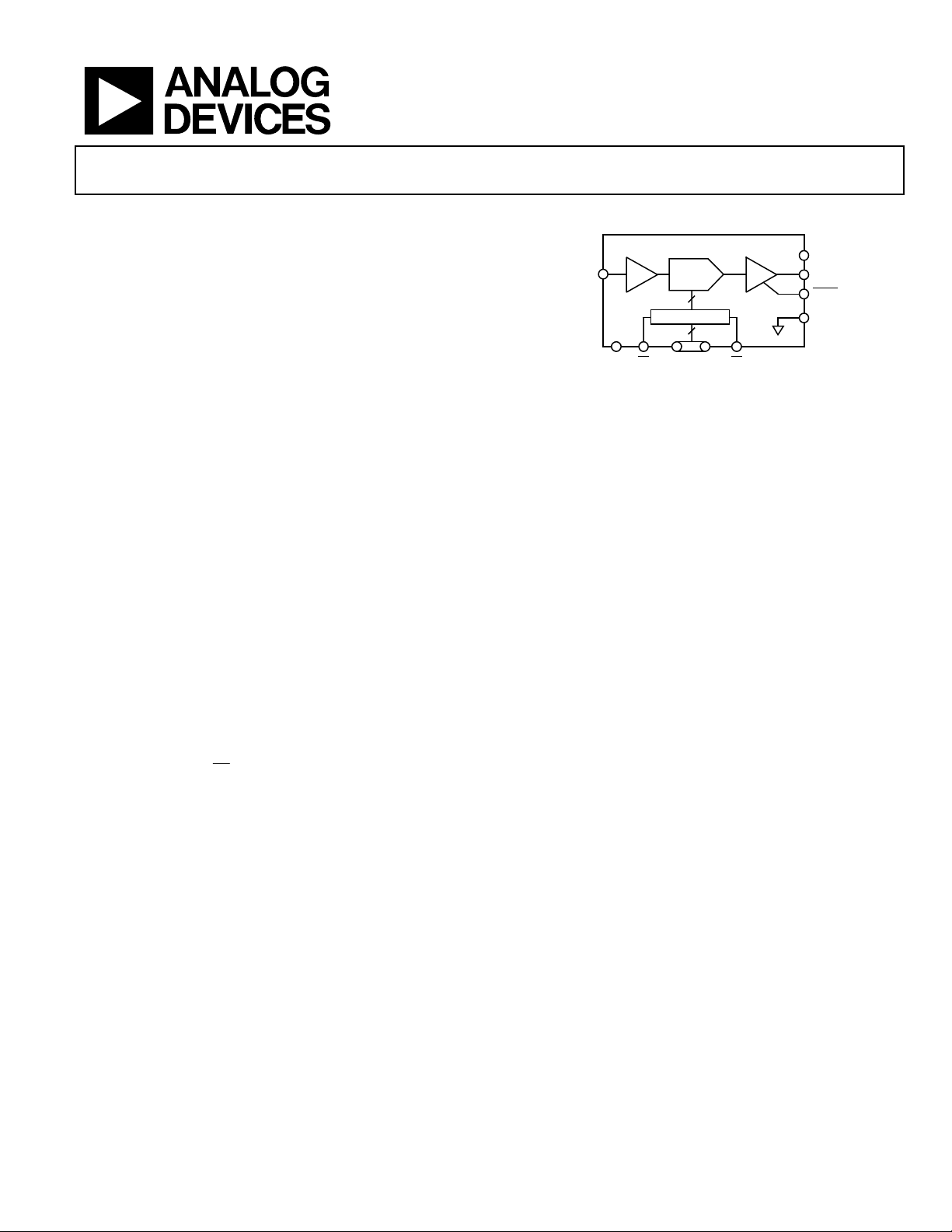
FUNCTIONAL BLOCK DIAGRAM
AD7392
V
REF
12-BIT
DAC
12
DAC REGISTER
12
Figure 1.
RSD0 TO D11CSDGND
Both parts are offered with similar pinouts, which allows users
to select the amount of resolution appropriate for their applications without changing the circuit card.
The AD7392/AD7393 are specified for operation over the
extended industrial temperature range of −40°C to +85°C.
The AD7393AR is specified for the automotive temperature
range of −40°C to +125°C. The AD7392/AD7393 are available
in 20-lead PDIP and 20-lead SOIC packages.
For serial data input, 8-lead packaged versions, see the AD7390
and AD7391.
V
DD
V
OUT
SHDN
AGND
1121 -0 01
Rev. C
Information furnished by Analog Devices is believed to be accurate and reliable. However, no
responsibility is assumed by Anal og Devices for its use, nor for any infringements of patents or ot her
rights of third parties that may result from its use. Specifications subject to change without notice. No
license is granted by implication or otherwise under any patent or patent rights of Analog Devices.
Trademarks and registered trademarks are the property of their respective owners.
One Technology Way, P.O. Box 9106, Norwood, MA 02062-9106, U.S.A.
Tel: 781.329.4700 www.analog.com
Fax: 781.461.3113 ©1996–2007 Analog Devices, Inc. All rights reserved.
Page 2

AD7392/AD7393
TABLE OF CONTENTS
Features.............................................................................................. 1
Applications....................................................................................... 1
Functional Block Diagram .............................................................. 1
General Description ......................................................................... 1
Revision History ............................................................................... 2
Specifications..................................................................................... 3
Electrical Characteristics ............................................................. 3
Timing Diagram........................................................................... 5
Absolute Maximum Ratings............................................................ 6
ESD Caution.................................................................................. 6
Pin Configurations and Function Descriptions ........................... 7
Typical Performance Characteristics ............................................. 8
Theory of Operation ...................................................................... 12
REVISION HISTORY
8/07—Rev. B to Rev. C
Changes to Specifications Section.................................................. 3
Changes to Table 3............................................................................ 6
Changes to Theory of Operation Section.................................... 12
Changes to Figure 29...................................................................... 13
Changes to Figure 32...................................................................... 14
Changes to Figure 33...................................................................... 15
Updated Outline Dimensions....................................................... 16
Changes to Ordering Guide.......................................................... 17
6/04—Changed from Rev. A to Rev. B
Removed TSSOP.................................................................Universal
Changes to Ordering Guide.......................................................... 17
3/99—Changed from Rev. 0 to Rev. A
11/96—Revision 0: Initial Version
Digital-to-Analog Converters................................................... 12
Amplifier Section ....................................................................... 12
Reference Input........................................................................... 12
Power Supply............................................................................... 13
Input Logic Levels ...................................................................... 13
Digital Interface.......................................................................... 13
Reset Pin (
Power Shutdown (
Unipolar Output Operation...................................................... 14
Bipolar Output Operation......................................................... 15
Outline Dimensions....................................................................... 16
Ordering Guide .......................................................................... 17
RS
) ............................................................................. 14
SHDN
)......................................................... 14
Rev. C | Page 2 of 20
Page 3
AD7392/AD7393
SPECIFICATIONS
ELECTRICAL CHARACTERISTICS
At V
= 2.5 V, −40°C < TA < +85°C, unless otherwise noted.
REF
Table 1. AD7392
Parameter Symbol Conditions 3 V ± 10% 5 V ± 10% Unit
STATIC PERFORMANCE
Resolution1 N 12 12 Bits
Relative Accuracy2 INL TA = +25°C ±1.8 ±1.8 LSB max
T
Differential Nonlinearity2 DNL TA = +25°C, monotonic ±0.9 ±0.9 LSB max
Monotonic ±1 ±1 LSB max
Zero-Scale Error V
Data = 0x000, TA = +25°C, +85°C 4.0 4.0 mV max
ZSE
Data = 0x000, TA = −40°C 8.0 8.0 mV max
Full-Scale Voltage Error V
TA = +25°C, +85°C, data = 0xFFF ±8 ±8 mV max
FSE
T
Full-Scale Temperature Coefficient3 TCVFS 28 28 ppm/°C typ
REFERENCE INPUT
V
Range V
REF
Input Resistance R
Input Capacitance3 C
0/VDD 0/VDD V min/max
REF
2.5 2.5 MΩ typ4
REF
5 5 pF typ
REF
ANALOG OUTPUT
Current (Source) I
Output Current (Sink) I
Data = 0x800, ∆ V
OUT
Data = 0x800, ∆ V
OUT
Capacitive Load3 CL No oscillation 100 100 pF typ
LOGIC INPUTS
Logic Input Low Voltage VIL 0.5 0.8 V max
Logic Input High Voltage VIH VDD − 0.6 VDD − 0.6 V min
Input Leakage Current IIL 10 10 μA max
Input Capacitance3 CIL 10 10 pF max
INTERFACE TIMING
3, 5
Chip Select Write Width tCS 45 45 ns min
Data Setup tDS 30 15 ns min
Data Hold tDH 20 5 ns min
Reset Pulse Width tRS 40 30 ns min
AC CHARACTERISTICS
Output Slew Rate SR Data = 0x000 to 0xFFF to 0x000 0.05 0.05 V/μs typ
Settling Time6 tS To ±0.1% of full scale 70 60 μs typ
Shutdown Recovery Time t
80 μs typ
SDR
DAC Glitch Code 0x7FF to Code 0x800 to Code 0x7FF 65 65 nV/s typ
Digital Feedthrough 15 15 nV/s typ
Feedthrough V
OUT/VREF
SUPPLY CHARACTERISTICS
Power Supply Range VDD
RANGE
Positive Supply Current IDD VIL = 0 V, no load 55/100 55/100 μA typ/max
Shutdown Supply Current I
Power Dissipation P
DD-SD
VIL = 0 V, no load 300 500 μW max
DISS
Power Supply Sensitivity PSS Δ VDD = ±5% 0.006 0.006 %/% max
1
One LSB = V
2
The first two codes (0x000, 0x001) are excluded from the linearity error measurement.
3
These parameters are guaranteed by design and not subject to production testing.
4
Typicals represent average readings measured at +25°C.
5
All input control signals are specified with tR = tF = 2 ns (10% to 90% of 13 V) and timed from a voltage level of 1.6 V.
6
The settling time specification does not apply for negative going transitions within the last 3 LSBs of ground.
/4096 V for the 12-bit AD7392.
REF
= −40°C, +85°C ±3 ±3 LSB max
A
= −40°C, data = 0xFFF ±20 ±20 mV max
A
= 5 LSB 1 1 mA typ
OUT
= 5 LSB 3 3 mA typ
OUT
V
= 1.5 V dc + 1 V p-p, data = 0x000,
REF
−63 −63 dB typ
f = 100 kHz
DNL < ±1 LSB 2.7/5.5 2.7/5.5 V min/max
SHDN
= 0, VIL = 0 V, no load
0.1/1.5 0.1/1.5 μA typ/max
Rev. C | Page 3 of 20
Page 4
AD7392/AD7393
At V
= 2.5 V, −40°C < TA < +85°C, unless otherwise noted.
REF
Table 2. AD7393
Parameter Symbol Conditions 3 V ± 10% 5 V ± 10% Unit
STATIC PERFORMANCE
Resolution1 N 10 10 Bits
Relative Accuracy2 INL TA = +25°C ±1.75 ±1.75 LSB max
T
Differential Nonlinearity2 DNL Monotonic ±0.8 ±0.8 LSB max
Zero-Scale Error V
Full-Scale Voltage Error V
Data = 0x000 9.0 9.0 mV max
ZSE
TA = +25°C, +85°C, +125°C, data = 0x3FF ±32 ±32 mV max
FSE
T
Full-Scale Temperature Coefficient3 TCVFS 28 28 ppm/°C typ
REFERENCE INPUT
V
Range V
REF IN
Input Resistance R
Input Capacitance3 C
0/VDD 0/VDD V min/max
REF
2.5 2.5 MΩ typ4
REF
5 5 pF typ
REF
ANALOG OUTPUT
Output Current (Source) I
Output Current (Sink) I
Data = 0x200, Δ V
OUT
Data = 0x200, Δ V
OUT
Capacitive Load3 CL No oscillation 100 100 pF typ
LOGIC INPUTS
Logic Input Low Voltage VIL 0.5 0.8 V max
Logic Input High Voltage VIH VDD − 0.6 VDD − 0.6 V min
Input Leakage Current IIL 10 10 μA max
Input Capacitance3 CIL 10 10 pF max
INTERFACE TIMING
3, 5
Chip Select Write Width tCS 45 45 ns
Data Setup tDS 30 15 ns
Data Hold tDH 20 5 ns
Reset Pulse Width tRS 40 30 ns
AC CHARACTERISTICS
Output Slew Rate SR Data = 0x000 to 0x3FF to 0x000 0.05 0.05 V/μs typ
Settling Time6 tS To ±0.1% of full scale 70 60 μs typ
Shutdown Recovery Time t
80 μs typ
SDR
DAC Glitch Code 0x7FF to Code 0x800 to Code 0x7FF 65 65 nV/s typ
Digital Feedthrough 15 15 nV/s typ
Feedthrough V
OUT/VREF
SUPPLY CHARACTERISTICS
Power Supply Range VDD
RANGE
Positive Supply Current IDD VIL = 0 V, no load, TA = +25°C 55 55 μA typ
V
Shutdown Supply Current I
Power Dissipation P
DD-SD
VIL = 0 V, no load 300 500 μW max
DISS
Power Supply Sensitivity PSS Δ VDD = ±5% 0.006 0.006 %/% max
1
One LSB = V
2
The first two codes (0x000, 0x001) are excluded from the linearity error measurement.
3
These parameters are guaranteed by design and not subject to production testing.
4
Typicals represent average readings measured at +25°C.
5
All input control signals are specified with tR = tF = 2 ns (10% to 90% of 13 V) and timed from a voltage level of 1.6 V.
6
The settling time specification does not apply for negative going transitions within the last 3 LSBs of ground.
/1024 V for the 10-bit AD7393.
REF
= −40°C, +85°C, +125°C ±2.0 ±2.0 LSB max
A
= −40°C, data = 0x3FF ±42 ±42 mV max
A
= 5 LSB 1 1 mA typ
OUT
= 5 LSB 3 3 mA typ
OUT
V
= 1.5 V dc 11 V p-p, data = 0x000, f = 100 kHz −63 −63 dB typ
REF
DNL < ±1 LSB 2.7/5.5 2.7/5.5 V min/max
= 0 V, no load 100 100 μA max
IL
SHDN
= 0, VIL = 0 V, no load
0.1/1.5 0.1/1.5 μA typ/max
Rev. C | Page 4 of 20
Page 5
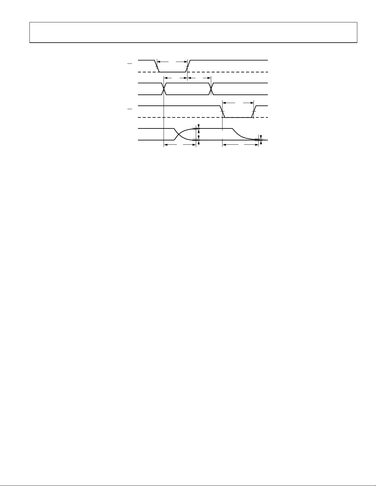
AD7392/AD7393
TIMING DIAGRAM
1
CS
0
1
D11 TO D0
0
1
RS
0
t
CS
t
DS
DATA VALID
t
DH
t
RS
FS
V
OUT
ZS
t
S
±0.1%FS
ERROR BAND
t
S
1121 -0 04
Figure 2. Timing Diagram
Rev. C | Page 5 of 20
Page 6
AD7392/AD7393
ABSOLUTE MAXIMUM RATINGS
Table 3.
Parameter Rating
VDD to GND −0.3 V, +8 V
V
to GND −0.3 V, VDD
REF
Logic Inputs to GND −0.3 V, VDD + 0.3 V
V
to GND −0.3 V, VDD + 0.3 V
OUT
I
Short Circuit to GND 50 mA
OUT
DGND to AGND −0.3 V, +2 V
Package Power Dissipation (TJ max − TA)/θJA
Thermal Resistance (θJA)
20-Lead PDIP (N 20) 57°C/W
20-Lead SOIC (R-20) 60°C/W
Maximum Junction Temperature (TJ max) 150°C
Operating Temperature Range −40°C to +85°C
AD7393AR −40°C to +125°C
Storage Temperature Range −65°C to +150°C
Lead Temperature
Reflow Soldering Peak Temperature
SnPb 240°C
Pb-Free 260°C
Stresses above those listed under Absolute Maximum Ratings
may cause permanent damage to the device. This is a stress
rating only; functional operation of the device at these or any
other conditions above those indicated in the operational
section of this specification is not implied. Exposure to absolute
maximum rating conditions for extended periods may affect
device reliability.
ESD CAUTION
Rev. C | Page 6 of 20
Page 7

AD7392/AD7393
PIN CONFIGURATIONS AND FUNCTION DESCRIPTIONS
1
V
DD
2
V
SHDN
DD
CS
RS
D0
D1
D2
D3
D4
D5
1
2
3
4
AD7392
5
TOP VIEW
6
(Not to Scale)
7
8
9
10
20
19
18
17
16
15
14
13
12
11
V
REF
V
OUT
AGND
DGND
D11
D10
D9
D8
D7
D6
01121-006
SHDN
3
CS
RS 4 DGND17
NC 5 D916
NC 6 D815
(Not to Scale)
D0 7 D714
D1 8 D613
D2 9 D512
10
D3
NC = NO CONNECT
Figure 3. AD7392 Pin Configuration Figure 4. AD7393 Pin Configuration
Table 4. AD7392 Pin Function Descriptions
Pin No. Mnemonic Description
1 VDD Positive Power Supply Input. The specified range of operation is 2.7 V to 5.5 V.
2
SHDN Power Shutdown Active Low Input. DAC register contents are saved as long as power stays on the VDD pin. When
SHDN = 0, CS strobes write new data into the DAC register.
3
4
CS
RS
Chip Select Latch Enable, Active Low.
Asynchronous Active Low Input. Resets the DAC register to 0.
5 to 16 D0 to D11 Parallel Input Data Bits. D11 is the MSB; D0 is the LSB.
17 DGND Digital Ground.
18 AGND Analog Ground.
19 V
20 V
DAC Voltage Output.
OUT
DAC Reference Input. Establishes the DAC full-scale voltage.
REF
AD7393
TOP VIEW
20
19
18
11
V
REF
V
OUT
AGND
D4
01121-007
Table 5. AD7393 Pin Function Descriptions
Pin No. Mnemonic Description
1 VDD Positive Power Supply Input. The specified range of operation is 2.7 V to 5.5 V.
2
3
4
SHDN Power Shutdown Active Low Input. DAC register contents are saved as long as power stays on the VDD pin.
SHDN = 0, CS strobes write new data into the DAC register.
When
CS
RS
Chip Select Latch Enable, Active Low.
Asynchronous Active Low Input. Resets the DAC register to 0.
5, 6 NC No Connect.
7 to 16 D0 to D9 Parallel Input Data Bits. D9 is the MSB; D0 is the LSB.
17 DGND Digital Ground.
18 AGND Analog Ground.
19 V
20 V
DAC Voltage Output.
OUT
DAC Reference Input. Establishes the DAC full-scale voltage.
REF
Rev. C | Page 7 of 20
Page 8

AD7392/AD7393
TYPICAL PERFORMANCE CHARACTERISTICS
1.0
AD7392
0.8
0.6
0.4
0.2
0
INL (LSB)
–0.2
–0.4
–0.6
–0.8
–1.0
0 512 1024 1536 2048 2560 3072 3584 4096
CODE (Decimal )
Figure 5. AD7392 Integral Nonlinearity Error vs. Code
1.0
AD7393
0.8
0.6
0.4
0.2
0
INL (LSB)
–0.2
–0.4
–0.6
–0.8
–1.0
0 128 256 384 512 640 768 896 1024
CODE (Decimal )
Figure 6. AD7393 Integral Nonlinearity Error vs. Code
VDD = 2.7V
V
= 2.5V
REF
T
= 25°C
A
VDD = 2.7V
V
= 2.5V
REF
T
= 25°C
A
100
90
80
70
60
50
40
FREQUENCY
30
20
10
01121-008
0
–10 –3.3 3.3 10 16 23 30 36 43 50
TOTAL UNADJUSTED ERROR (LSB)
AD7393
SS = 300 UNITS
V
= 2.7V
DD
V
= 2.5V
REF
T
= 25°C
A
01121-011
Figure 8. AD7393 Total Unadjusted Error Histogram
30
AD7393
SS = 100 UNITS
V
= 2.7V
DD
24
V
= 2.5V
REF
T
= –40°C TO +85° C
A
18
12
FREQUENCY
6
01121-009
0
–66 0–6–12–20–26–32–40–46–52–60
FULL-SCAL E TEMPERATURE COEFFICIENT (ppm/° C)
01121-012
Figure 9. AD7393 Full-Scale Output Temperature Coefficient Histogram
25
AD7392
SS = 100 UNITS
V
= 2.7V
DD
20
V
= 2.5V
REF
T
= 25°C
A
15
10
FREQUENCY
5
0
5.0 5.8 6.6 7. 3 8.1 8.9 9.7 10.5 11.2 12.0
TOTAL UNADJUSTED ERROR (LSB)
Figure 7. AD7392 Total Unadjusted Error Histogram
01121-010
Rev. C | Page 8 of 20
16
14
12
10
8
6
4
OUTPUT VOLTAGE NOISE (µV/ Hz)
2
0
1 10 100 1k 10k 100k
FREQUENCY (Hz)
AD7392
VDD = 5V
V
T
Figure 10. Voltage Noise Density vs. Frequency
REF
= 25°C
A
= 2.5V
01121-013
Page 9

AD7392/AD7393
100
AD7392
95
VDD = 3V
T
= 25°C
A
90
85
80
75
70
65
SUPPLY CURRENT (µA)
60
55
50
V
FROM
LOGIC
3V TO 0V
0
VIN (V)
Figure 11. Supply Current vs. Logic Input Voltage
FROM
V
LOGIC
0V TO 3V
01121-014
3.02.52.01.51.00.5
1000
AD7392
V
= 0V TO VDDTO 0V
LOGIC
V
= 2.5V
REF
800
T
= 25°C
A
600
400
SUPPLY CURRENT (µA)
200
= 5.5V, CODE = 0x155
a. V
DD
b. V
= 5.5V, CODE = 0x3FF
DD
c. V
= 2.7V, CODE = 0x155
DD
d. V
= 2.7V, CODE = 0x355
DD
0
1k 10k 100k 1M 10M
CLOCK FREQ UENCY (Hz)
c
Figure 14. Supply Current vs. Clock Frequency
a
b
d
01121-017
5.0
AD7392
4.5
CODE = 0xFFF
V
= 2V
REF
4.0
RS LOGI C VOLTAGE
VARIED
3.5
3.0
2.5
2.0
1.5
THRESHOLD VOLTAGE (V)
1.0
0.5
0
1765432
V
LOGIC
HIGH TO LOW
Figure 12. Logic Threshold vs. Supply Voltage
100
AD7392
SAMPLE SIZE = 300 UNITS
90
80
VDD = 3.6V, V
70
60
50
SUPPLY CURRENT (µA)
40
FROM
SUPPLY VOLTAGE (V)
VDD = 5V, V
= 2.4V
LOGIC
V
FROM
LOGIC
LOW TO HIGH
= 0V
LOGIC
= 3V, V
V
DD
LOGIC
= 0V
60
50
40
30
PSRR (dB)
20
10
01121-015
0
10 100 1k 10k
V
DD
VDD = 5V ± 5%
= 3V ± 5%
FREQUENCY (Hz)
TA = 25°C
01121-018
Figure 15. Power Supply Rejection Ratio vs. Frequency
40
30
20
(mA)
OUT
I
10
VDD = 5V
= 3V
V
REF
CODE = 0x000
30
20
–55 –35 –15 5 25 45 65 85 105 125
TEMPERATURE ( °C)
Figure 13. Supply Current vs. Temperature
01121-016
Rev. C | Page 9 of 20
0
054321
Figure 16. I
V
(V)
OUT
at Zero Scale vs. V
OUT
OUT
01121-019
Page 10

AD7392/AD7393
5
2µs
V
OUT
(5mV/DIV)
CS
(5V/DIV)
20mV
TIME (2µs/DIV)
VDD = 5V
V
f
CODE: 0x7F TO 0x80
Figure 17. Midscale Transition Performance
CLK
REF
= 2.5V
= 50kHz
AD7392
0
–5
VDD = 5V
= 100mV + 2V
V
REF
–10
DATA = 0xFFF
–15
GAIN (dB)
–20
–25
01121-020
–30
10 100 1k 10k 100k
DC
FREQUENCY (Hz)
01121-023
Figure 20. Reference Multiplying Bandwidth
5µs
V
OUT
(5mV/DIV)
5mV
TIME (5µs/DIV)
Figure 18. Digital Feedthrough
100µs
V
OUT
(1V/DIV)
VDD = 5V
V
REF
CS = HIGH
D0 TO D11
(5V/DIV)
AD7392
= 2.5V
2.0
1.8
1.6
1.4
1.2
1.0
INL (LSB)
0.8
0.6
0.4
0.2
01121-021
0
01234
REFERENCE VO LTAGE (V)
AD7392
VDD = 5V
CODE = 0x768
= 25°C
T
A
01121-024
5
Figure 21. Integral Nonlinearity Error vs. Reference Voltage
1.2
1.0
0.8
0.6
AD7392
SAMPLE SIZE = 50
CODE = 0xFF F
CS
(5V/DIV)
1V
TIME (100µ s/DIV)
Figure 19. Large Signal Settling Time
VDD = 5V
V
REF
= 2.5V
01121-022
Rev. C | Page 10 of 20
0.4
0.2
NOMINAL CHANGE I N VOLTAGE (mV)
0
0 100 200 300 400 500 600
HOURS OF OP ERATION AT 150°C
CODE = 0x000
Figure 22. Long-Term Drift Accelerated by Burn-In
01121-025
Page 11

AD7392/AD7393
V
I
DD
OUT
(µA)
(V)
SHDN
100
5V 500mV
100
90
50
0
2
0
1
10
0%
0
2V
VDD = 5V
V
CODE = 0xFFF
RL = 1MΩ TO GND
T
TIME (100µs/DIV)
Figure 23. Shutdown Recovery Time
REF
= 25°C
A
= 2.5V
AD7392
100µs
1.0
AD7392
0.8
0.6
0.4
0.2
0
DNL (LS B)
–0.2
–0.4
–0.6
–0.8
01121-026
–1.0
0 512 1024 1536 2048 2560 3072 3584 4096
CODE (Decimal )
Figure 25. AD7392 Differential Nonlinearity Error vs. Code
VDD = 2.7V
= 2.5V
V
REF
= 25°C
T
A
01121-002
1000
AD7392
100
SUPPLY CURRENT (nA)
VDD = 5.5V
= 2.5V
V
REF
SHDN = 0V
10
–55 –35 –15 5 25 45 65 85 105 125
TEMPERATURE (°C)
01121-027
Figure 24. Shutdown Current vs. Temperature
1.0
AD7393
0.8
0.6
0.4
0.2
0
DNL (LS B)
–0.2
–0.4
–0.6
–0.8
–1.0
0 128 256 384 512 640 768 896 1024
CODE (Decimal )
Figure 26. AD7393 Differential Nonlinearity Error vs. Code
VDD = 2.7V
= 2.5V
V
REF
= 25°C
T
A
01121-003
Rev. C | Page 11 of 20
Page 12

AD7392/AD7393
V
THEORY OF OPERATION
The AD7392/AD7393 comprise a set of pin-compatible, 12-/10bit digital-to-analog converters (DACs). These single-supply
operation devices consume less than 100 μA of current while
operating from 2.7 V to 5.5 V power supplies, making them
ideal for battery-operated applications. They contain a voltageswitched, 12-/10-bit, laser-trimmed DAC; rail-to-rail output op
amps; and a parallel input DAC register. The external reference
input has constant input resistance independent of the digital
code setting of the DAC. In addition, the reference input can be
tied to the same supply voltage as V
output voltage span of 0 V to V
consists of a
CS
write strobe and 12 data bits (D0 to D11) if
, resulting in a maximum
DD
. The parallel data interface
DD
utilizing the AD7392 or 10 data bits (D0 to D9) if utilizing
the AD7393. An
RS
pin is available to reset the DAC register to
zero scale. This function is useful for power-on reset or system
failure recovery to a known state. Additional power savings are
accomplished by activating the
SHDN
pin, resulting in a 1.5 μA
maximum consumption sleep mode. While the supply voltage is
on, data is retained in the DAC register to reset the DAC output
when the part is taken out of shutdown (
SHDN
= 1).
DIGITAL-TO-ANALOG CONVERTERS
The voltage switched R-2R DAC generates an output voltage
that depends on the external reference voltage connected to
the V
where:
D is the decimal data-word loaded into the DAC register.
N is the number of bits of DAC resolution.
If the 10-bit AD7393 uses a 2.5 V reference, Equation 1
becomes
Using Equation 2, the nominal midscale voltage at V
1.25 V, for
step size is 2.5 × 1/1024 = 0.0024 V.
If the 12-bit AD7392 uses a 5.0 V reference, Equation 1
becomes
Using Equation 3, the AD7392 provides a nominal midscale voltage of 2.50 V (for
The LSB step size is 5.0 × 1/4096 = 0.0012 V.
pin according to Equation 1.
REF
D
VV
×=
REF
OUT
OUT
5.2
V
(1)
N
2
D
×= (2)
1024
D = 512; full-scale voltage is 2.497 V. The LSB
OUT
VV
D
×= (3)
REF
4096
D = 2048) and a full-scale V
of 4.998 V.
OUT
OUT
is
AMPLIFIER SECTION
The internal DACs output is buffered by a low power consumption precision amplifier. The op amp has a 60 μs typical settling
time to 0.1% of full scale. There are slight differences in settling
time for negative slew signals vs. positive. Also, negative transition settling time to within the last 6 LSBs of 0 V has an extended
settling time. The rail-to-rail output stage of this amplifier has
been designed to provide precision performance while operating
near either power supply.
Figure 27 shows an equivalent output
schematic of the rail-to-rail amplifier with its N-channel pulldown FETs that pull an output load directly to GND. The
output sourcing current is provided by a P-channel, pull-up
device that can source current-to-GND terminated loads.
P-CH
N-CH
Figure 27. Equivalent Analog Output Circuit
DD
V
OUT
AGND
01121-028
The rail-to-rail output stage provides ±1 mA of output current.
The N-channel output pull-down MOSFET, shown in
Figure 27,
has a 35 Ω on resistance that sets the sink current capability
near ground. In addition to resistive load driving capability, the
amplifier also has been carefully designed and characterized for
up to 100 pF capacitive load driving capability.
REFERENCE INPUT
The reference input terminal has a constant input resistance
independent of digital code, which results in reduced glitches
on the external reference voltage source. The high 2.5 MΩ input
resistance minimizes power dissipation within the AD7392/
AD7393 DACs. The V
from ground to the positive supply voltage V
simplest applications for saving an external reference voltage
source is connecting the REF terminal to the positive V
supply. This connection results in a rail-to-rail voltage output
span maximizing the programmed range. The reference input
accepts ac signals as long as they stay within the 0 V < V
supply voltage range. The reference bandwidth and integral
V
DD
nonlinearity error performance are plotted in
Figure 21. The ratiometric reference feature makes the AD7392/
AD7393 an ideal companion to ratiometric analog-to-digital
converters (ADCs) such as the AD7896.
input accepts input voltages ranging
REF
. One of the
DD
Figure 20 and
DD
REF
<
Rev. C | Page 12 of 20
Page 13

AD7392/AD7393
V
POWER SUPPLY
The very low power consumption of the AD7392/AD7393 is
a direct result of a circuit design that optimizes the CBCMOS
process. By using the low power characteristics of CMOS for the
logic and the low noise, tight-matching of the complementary
bipolar transistors, excellent analog accuracy is achieved. One
advantage of the rail-to-rail output amplifiers used in the AD7392/
AD7393 is the wide range of usable supply voltage. The part is
fully specified and tested for operation from 2.7 V to 5.5 V.
FERRITE BEAD:
2 TURNS, FAIR-RITE
TTL/CMOS
LOGIC
CIRCUITS
5V
POWER SUPPLY
#2677006301
+
100µF
ELECT.
+
10µF TO 22µF
TAN T.
+
0.1µF
CER.
5V
5V
RETURN
01121-029
Figure 28. Use Separate Traces to Reduce Power Supply Noise
Whether or not a separate power supply trace is available, generous supply bypassing reduces supply line induced errors. Local
supply bypassing, consisting of a 10 μF tantalum electrolytic in
parallel with a 0.1 μF ceramic capacitor, is recommended for all
applications (see Figure 29).
2.7VTO 5.5V
*
C
D0 TO D11
* OPTIONAL EXTERNAL
REFERENCE BYPASS
20
V
REF
AD7392
AD7393
2
SHDN
3
CS
4
RS
Figure 29. Recommended Supply Bypassing for the AD7392/AD7393
OR
GND
17, 18
1
V
DD
0.1µF
+
10µF
19
V
OUT
01121-030
INPUT LOGIC LEVELS
All digital inputs are protected with a Zener-type ESD protection
structure that allows logic input voltages to exceed the V
voltage (see Figure 30). This feature is useful if the user is driving
one or more of the digital inputs with a 5 V CMOS logic input
voltage level while operating the AD7392/AD7393 on a 3 V
power supply. If this interface is used, make sure that the V
of the 5 V CMOS meets the V
input requirement of the AD7392/
IL
AD7393 operating at 3 V. See Figure 12 for a graph of digital
logic input threshold vs. operating V
DD
LOGIC
GND
Figure 30. Equivalent Digital Input ESD Protection
1kΩ
IN
supply voltage.
DD
01121-031
supply
DD
OL
To minimize power dissipation from input logic levels that
are near the V
and VIL logic input voltage specifications, a
IH
Schmitt-trigger design was used that minimizes the input
buffer current consumption compared to traditional CMOS
input stages. Figure 11 is a plot of supply current vs. incremental
input voltage, showing that negligible current consumption
takes place when logic levels are in their quiescent state. The
normal crossover current still occurs during logic transitions.
A secondary advantage of this Schmitt trigger is the prevention
of false triggers that would occur with slow moving logic transitions when a standard CMOS logic interface or opto-isolators
are used. Logic inputs D11 to D0,
CS
, RS, and
SHDN
all contain
the Schmitt-trigger circuits.
DIGITAL INTERFACE
The AD7392/AD7393 have a parallel data input. A functional
block diagram of the digital section is shown in Figure 31,
while Table 6 contains the truth table for the logic control
inputs. The chip select pin (
the data inputs on Pin D11 to Pin D0. This active low input
places the input register into a transparent state allowing the
data inputs to directly change the DAC ladder values. When
CS
returns to logic high within the data setup-and-hold time
specifications, the new value of data in the input register are
latched. See Table 6 for a complete listing of conditions.
Dx
CS
RS
Figure 31. Digital Control Logic
Table 6. Control Logic Truth Table
CS
DAC Register Function
RS
H H Latched
L H Transparent
↑1
H Latched with new data
X2 L Loaded with all zeros
H
1
↑ = Positive logic transition.
2
X = Don’t care.
1
↑
Latched all zeros
CS
) controls loading of data from
1 OF 12 LATCHES
OF THE
DAC REGISTER
TO
INTERNAL
DAC SWITCHES
01121-005
Rev. C | Page 13 of 20
Page 14

AD7392/AD7393
RESET PIN (RS)
Forcing the asynchronous RS pin low sets the DAC register to
all 0s, so the DAC output voltage is 0 V. The reset function is
useful for setting the DAC outputs to 0 at power-up or after a
power supply interruption. Test systems and motor controllers
are two of many applications that benefit from powering up to a
known state. The external reset pulse can be generated by three
methods:
• The microprocessor’s power-on RESET signal
• An output from the microprocessor
• An external resistor and capacitor
RESET has a Schmitt-trigger input, which results in a clean
reset function when using external resistor-/capacitor-generated
pulses (see
Tabl e 6 ).
POWER SHUTDOWN (SHDN)
Maximum power savings can be achieved by using the power
shutdown control function. This hardware-activated feature is
controlled by the active low input
Schmitt-trigger input that helps desensitize it to slowly changing
inputs. Setting this pin to logic low reduces the internal consumption of the AD7392/AD7393 to nanoamp levels, guaranteed
to 1.5 μA maximum over the operating temperature range. If
power is present at all times on the V
mode, the internal DAC register retains the last programmed
data value. The digital interface is still active in shutdown so
that code changes can be made that produce new DAC settings
when the device is taken out of shutdown. This data is used
when the part is returned to the normal active state by placing
the DAC back to its programmed voltage setting.
shows a plot of shutdown recovery time with both I
displayed. In the shutdown state, the DAC output amplifier
exhibits an open-circuit high resistance state. Any load that is
connected stabilizes at its termination voltage. If the power
shutdown feature is not needed, the user should tie the
pin to the V
voltage to disable this function.
DD
SHDN
pin. This pin has a
pin while in shutdown
DD
Figure 23
and V
DD
SHDN
OUT
UNIPOLAR OUTPUT OPERATION
This is the basic mode of operation for the AD7392. The
AD7392 is designed to drive loads as low as 5 kΩ in parallel
with 100 pF (see
shown in
The circuit can be configured with an external reference
plus power supply or powered from a single dedicated regulator or reference depending on the application performance
requirements.
EXT
REF
NOTES
1. DIGITAL INTERFACE CIRCUITRY OMI TTED FO R CLARITY
Table 7. Unipolar Code Table
DAC Register No.
Hexadecimal Decimal Output Voltage (V), V
0xFFF 4095 2.4994
0x801 2049 1.2506
0x800 2048 1.2500
0x7FF 2047 1.2494
0x000 0 0
Figure 32). The code table for this operation is
Tabl e 7 .
2.7VTO 5.5V
R
AD7392
V
REF
V
GND
1
DD
17, 18
V
OUT
0.01µF
20
Figure 32. AD7392 Unipolar Output Operation
0.1µF
19
R
≥5kΩ
10µF
C
L
L
≥100pF
01121-032
= 2.5 V
REF
Rev. C | Page 14 of 20
Page 15

AD7392/AD7393
V
A
BIPOLAR OUTPUT OPERATION
Although the AD7393 is designed for single-supply operation,
the output can be easily configured for bipolar operation. A
typical circuit is shown in
regulated 5 V supply for power, which also provides the circuit’s
reference voltage. Since the AD7393 output span swings from
ground to very near 5 V, it is necessary to choose an external
amplifier with a common-mode input voltage range that extends
to its positive supply rail. The micropower consumption OP196
is designed just for this purpose and results in only 50 μA of
maximum current consumption. Connecting the two 470 kΩ
resistors results in a differential amplifier mode of operation
with a voltage gain of 2, which produces a circuit output span
of 10 V, that is, −5 V to +5 V. As the DAC is programmed from
zero-code 0x000 to midscale 0x200 to full scale 0x3FF, the circuit
output voltage, V
O
The output voltage, V
Equation 4.
⎡
⎢
⎣
512
−=DV
O
D is the decimal code loaded in the AD7393 DAC
where
register.
Note that the LSB step size is 10/1024 = 10 mV. This circuit
is optimized for micropower consumption including the 470 kΩ
gain setting resistors, which should have low temperature
coefficients to maintain accuracy and matching (preferably the
same resistor material, such as metal film).
If better stability is required, the power supply may be substituted with a precision reference voltage such as the low dropout
REF195, which can easily supply the circuit’s 162 μA of current,
and still provide additional power for the load connected to V
The micropower REF195 is guaranteed to source 10 mA output
drive current, but consumes only 50 μA internally.
Figure 33. This circuit uses a clean,
, is set at −5 V, 0 V, and +5 V (minus 1 LSB).
, is coded in offset binary according to
O
⎤
51
×
(4)
⎥
⎦
O
.
If higher resolution is required, the AD7392 can be used with
two additional bits of data inserted into the software coding,
which results in a 2.5 mV LSB step size.
of nominal output voltages (V
) provided by the bipolar
O
Tabl e 8 shows examples
operation circuit application.
I
<162µ
SY
+5
C
NOTES
1. DIGITAL INTERFACE CIRCUIT RY OMITT ED FOR CL ARITY
<2µA
V
REF
AD7393
Figure 33. Bipolar Output Operation
GND
470kΩ 470kΩ
V
DD
V
OUT
OP196
–5V
<50µA<100µA
V
O
+5V
–5V
BIPOLAR
OUTPUT
SWING
Table 8. Bipolar Code Table
DAC Register No.
Hexadecimal Decimal Analog Output Voltage (V)
0x3FF 1023 +4.9902
0x201 513 +0.0097
0x200 512 0.0000
0x1FF 511 −0.0097
0x000 0 −5.0000
01121-033
Rev. C | Page 15 of 20
Page 16

AD7392/AD7393
OUTLINE DIMENSIONS
1.060 (26.92)
1.030 (26.16)
0.980 (24.89)
0.210 (5.33)
0.150 (3.81)
0.130 (3.30)
0.115 (2.92)
0.022 (0.56)
0.018 (0.46)
0.014 (0.36)
MAX
20
1
0.100 (2.54)
BSC
0.070 (1.78)
0.060 (1.52)
0.045 (1.14)
11
10
0.280 (7.11)
0.250 (6.35)
0.240 (6.10)
0.015
(0.38)
MIN
SEATING
PLANE
0.005 (0.13)
MIN
0.060 (1.52)
MAX
0.015 (0.38)
GAUGE
PLANE
0.325 (8.26)
0.310 (7.87)
0.300 (7.62)
0.430 (10.92)
MAX
0.195 (4.95)
0.130 (3.30)
0.115 (2.92)
0.014 (0.36)
0.010 (0.25)
0.008 (0.20)
CONTROLL ING DIMENSI ONS ARE IN INCHES; MILLIMETER DIMENSIONS
(IN PARENTHESES) ARE ROUNDED-OF F INCH EQUI VALENTS FOR
REFERENCE ONLY AND ARE NOT APPROPRIATE FOR USE I N DESIGN.
CORNER LEADS MAY BE CONFIGURED AS WHOLE OR HALF LEADS.
COMPLIANT TO JEDEC STANDARDS MS-001
070706-A
Figure 34. 20-Lead Plastic Dual In-Line Package [PDIP]
Narrow Body
(N-20)
Dimensions shown in inches and (millimeters)
13.00 (0.5 118)
12.60 (0.4961)
11
7.60 (0.2992)
7.40 (0.2913)
10
10.65 (0.4193)
10.00 (0.3937)
2.65 (0.1043)
2.35 (0.0925)
SEATING
PLANE
8°
0°
0.33 (0.0130)
0.20 (0.0079)
0
0
.
7
.
2
(
0
5
5
(
0
.
0
2
9
5
)
9
8
)
.
0
0
1.27 (0.0500)
0.40 (0.0157)
45°
060706-A
0.30 (0.0118)
0.10 (0.0039)
COPLANARITY
0.10
20
1
0.51 (0.0201)
1.27
(0.0500)
CONTROLL ING DIMENSIONS ARE IN MILLI METERS; INCH DIMENSIONS
(IN PARENTHESES) ARE ROUNDED-O FF MIL LIMETER EQUIVALENTS FOR
REFERENCE ON LY AND ARE NOT APPROPRI ATE FOR USE IN DESIGN.
0.31 (0.0122)
BSC
COMPLIANT TO JEDEC STANDARDS MS-013-AC
Figure 35. 20-Lead Standard Small Outline Package [SOIC_W]
Wide Body
(RW-20)
Dimensions shown in millimeters and (inches)
Rev. C | Page 16 of 20
Page 17

AD7392/AD7393
ORDERING GUIDE
Model Resolution (Bits) Temperature Range Package Description Package Option
AD7392AN 12 −40°C to +85°C 20-Lead PDIP N-20
AD7392ANZ
AD7392AR 12 −40°C to +85°C 20-Lead SOIC_W RW-20
AD7392AR-REEL 12 −40°C to +85°C 20-Lead SOIC_W RW-20
AD7392ARZ
AD7392ARZ-REEL
AD7393AN 10 −40°C to +85°C 20-Lead PDIP N-20
AD7393AR 10 −40°C to +125°C 20-Lead SOIC_W RW-20
AD7393ARZ
1
Z = RoHS Compliant Part.
1
1
1
1
12 −40°C to +85°C 20-Lead PDIP N-20
12 −40°C to +85°C 20-Lead SOIC_W RW-20
12 −40°C to +85°C 20-Lead SOIC_W RW-20
10 −40°C to +125°C 20-Lead SOIC_W RW-20
Rev. C | Page 17 of 20
Page 18

AD7392/AD7393
NOTES
Rev. C | Page 18 of 20
Page 19

AD7392/AD7393
NOTES
Rev. C | Page 19 of 20
Page 20

AD7392/AD7393
NOTES
©1996–2007 Analog Devices, Inc. All rights reserved. Trademarks and
registered trademarks are the property of their respective owners.
C01121-0-8/07(C)
Rev. C | Page 20 of 20
 Loading...