

Page 1
True Bipolar Input, Dual 12-Bit/14-Bit,
AD7366/AD7367
12-/14-BIT
SUCCESSIVE
APPROXIMATION
ADC
D
OUT
A
OUTPUT
DRIVERS
CONTROL
LOGIC
T/H
BUF
V
A1
V
A2
MUX
REF
AD7366/AD7367
V
DRIVE
D
CAP
A AV
CC
DV
CC
BUF
D
OUT
B
OUTPUT
DRIVERS
12-/14-BIT
SUCCESSIVE
APPROXIMATION
ADC
T/H
V
B1
V
B2
AGND AGND V
SS
DGNDD
CAP
B
CS
SCLK
CNVST
BUSY
ADDR
RANGE0
RANGE1
REFSEL
MUX
V
DD
06703-001
FEATURES
Dual 12-bit/14-bit, 2-channel ADC
Tru e bipolar analog inputs
Programmable input ranges:
±10 V, ±5 V, 0 V to 10 V
±12 V with 3 V external reference
Throughput rate: 1 MSPS
Simultaneous conversion with read in less than 1 μs
High analog input impedance
Low current consumption:
8.3 mA typical in normal mode
320 nA typical in shutdown mode
AD7366
72 dB SNR at 50 kHz input frequency
12-bit no missing codes
AD7367
76 dB SNR at 50 kHz input frequency
14-bit no missing codes
Accurate on-chip reference: 2.5 V ± 0.2%
−40°C to +85°C operation
High speed serial interface
Compatible with SPI®, QSPI™, MICROWIRE™, and DSP
iCMOS® process technology
Available in a 24-lead TSSOP
2-Channel, Simultaneous Sampling SAR ADC
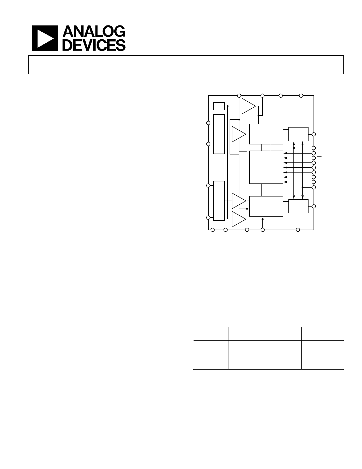
FUNCTIONAL BLOCK DIAGRAM
Figure 1.
GENERAL DESCRIPTION
1
The AD7366/AD7367
power, successive approximation analog-to-digital converters
(ADCs) that feature throughput rates up to 1 MSPS. The device
contains two ADCs, each preceded by a 2-channel multiplexer,
and a low noise, wide bandwidth track-and-hold amplifier.
The AD7366/AD7367 are fabricated on the Analog Devices, Inc.,
industrial CMOS process (iCMOS
platform combining the advantages of low and high voltage
CMOS. The iCMOS process allows the AD7366/AD7367 to
accept high voltage bipolar signals in addition to reducing
power consumption and package size. The AD7366/AD7367
can accept true bipolar analog input signals in the ±10 V range,
±5 V range, and 0 V to 10 V range.
The AD7366/AD7367 have an on-chip 2.5 V reference that
can be disabled to allow the use of an external reference.
If a 3 V reference is applied to the D
AD7366/AD7367 can accept a true bipolar ±12 V analog input.
Minimum ±12 V V
±12 V input range.
Rev. D
Information furnished by Analog Devices is believed to be accurate and reliable. However, no
responsibility is assumed by Analog Devices for its use, nor for any infringements of patents or other
rights of third parties that may result from its use. Specifications subject to change without notice. No
license is granted by implication or otherwise under any patent or patent rights of Analog Devices.
Trademarks and registered trademarks are the property of their respective owners.
are dual 12-bit/14-bit, high speed, low
2
), which is a technology
DD
and VSS supplies are required for the
A and D
CAP
B pins, the
CAP
PRODUCT HIGHLIGHTS
1. The AD7366/AD7367 can accept true bipolar analog input
signals, as well as ±10 V, ±5 V, ±12 V (with external reference), and 0 V to 10 V unipolar signals.
2. Two complete ADC functions allow simultaneous sampling
and conversion of two channels.
3. 1 MSPS serial interface: SPI-/QSPI-/DSP-/MICROWIRE-
compatible interface.
Table 1. Related Products
Throughput
Device Resolution
Rate
AD7366 12-Bit 1 MSPS Dual, 2-channel
AD7366-5 12-Bit 500 kSPS Dual, 2-channel
AD7367 14-Bit 1 MSPS Dual, 2-channel
AD7367-5 14-Bit 500 kSPS Dual, 2-channel
1
Protected by U.S. Patent No. 6,731,232.
2
iCMOS Process Technology. For analog systems designers within
industrial/instrumentation equipment OEMs who need high performance
ICs at higher voltage levels, iCMOS is a technology platform that enables the
development of analog ICs capable of 30 V and operating at ±15 V supplies
while allowing dramatic reductions in power consumption and package size,
and increased ac and dc performance.
One Technology Way, P.O. Box 9106, Norwood, MA 02062-9106, U.S.A.
Tel: 781.329.4700
Fax: 781.461.3113 ©2007-2010 Analog Devices, Inc. All rights reserved.
Number of
Channels
www.analog.com
 Loading...