

Page 1
10 MHz, 4-Quadrant
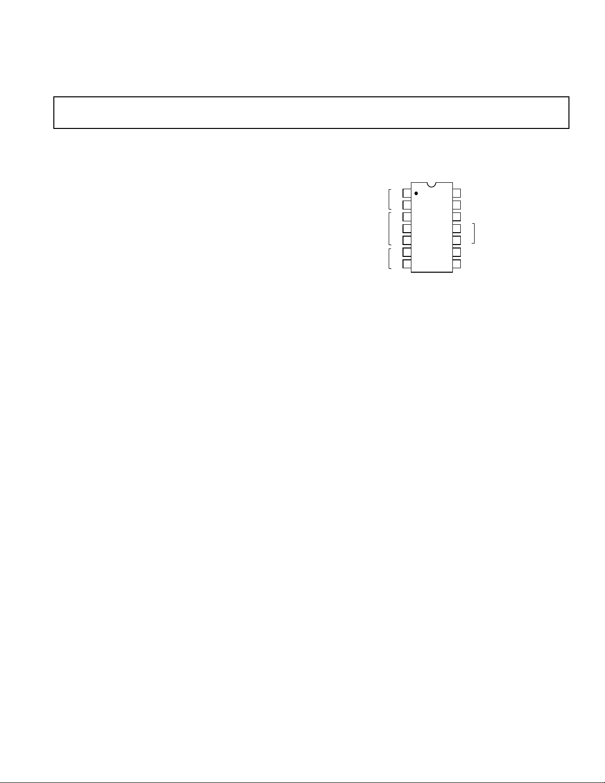
14
13
12
11
10
9
8
1
2
3
4
7
6
5
TOP VIEW
(Not to Scale)
X1
Z1
W OUTPUT
DD DENOMINATOR DISABLE
VP POSITIVE SUPPLY
X2
U0
U1
AD734
VN NEGATIVE SUPPLY
ER REFERENCE VOLTAGE
Z2
U2
Y1
Y2
Z INPUT
X INPUT
DENOMINATOR
INTERFACE
Y INPUT
a
FEATURES
High Accuracy
0.1% Typical Error
High Speed
10 MHz Full-Power Bandwidth
450 V/s Slew Rate
200 ns Settling to 0.1% at Full Power
Low Distortion
–80 dBc from Any Input
Third-Order IMD Typically –75 dBc at 10 MHz
Low Noise
94 dB SNR, 10 Hz to 20 kHz
70 dB SNR, 10 Hz to 10 MHz
Direct Division Mode
2 MHz BW at Gain of 100
APPLICATIONS
High Performance Replacement for AD534
Multiply, Divide, Square, Square Root
Modulator, Demodulator
Wideband Gain Control, RMS-DC Conversion
Voltage-Controlled Amplifiers, Oscillators, and Filters
Demodulator with 40 MHz Input Bandwidth
PRODUCT DESCRIPTION
The AD734 is an accurate high speed, four-quadrant analog
multiplier that is pin-compatible with the industry-standard
AD534 and provides the transfer function W = XY/U. The
AD734 provides a low-impedance voltage output with a fullpower (20 V pk-pk) bandwidth of 10 MHz. Total static error
(scaling, offsets, and nonlinearities combined) is 0.1% of full
scale. Distortion is typically less than –80 dBc and guaranteed.
The low capacitance X, Y and Z inputs are fully differential. In
most applications, no external components are required to
define the function.
The internal scaling (denominator) voltage U is 10 V, derived
from a buried-Zener voltage reference. A new feature provides
the option of substituting an external denominator voltage,
allowing the use of the AD734 as a two-quadrant divider with a
1000:1 denominator range and a signal bandwidth that remains
10 MHz to a gain of 20 dB, 2 MHz at a gain of 40 dB and
200 kHz at a gain of 60 dB, for a gain-bandwidth product of
200 MHz.
The advanced performance of the AD734 is achieved by a
combination of new circuit techniques, the use of a high speed
complementary bipolar process and a novel approach to lasertrimming based on ac signals rather than the customary dc
methods. The wide bandwidth (>40 MHz) of the AD734’s
input stages and the 200 MHz gain-bandwidth product of the
multiplier core allow the AD734 to be used as a low distortion
Multiplier/Divider
AD734
CONNECTION DIAGRAM
14-Lead DIP
(Q Package and N Package)
demodulator with input frequencies as high as 40 MHz as long
as the desired output frequency is less than 10 MHz.
The AD734AQ and AD734BQ are specified for the industrial
temperature range of –40°C to +85°C and come in a 14-lead
ceramic DIP. The AD734SQ/883B, available processed to
MIL-STD-883B for the military range of –55°C to +125°C, is
available in a 14-lead ceramic DIP.
PRODUCT HIGHLIGHTS
The AD734 embodies more than two decades of experience in
the design and manufacture of analog multipliers, to provide:
1. A new output amplifier design with more than twenty times
the slew-rate of the AD534 (450 V/µs versus 20 V/µs) for a
full power (20 V pk-pk) bandwidth of 10 MHz.
2. Very low distortion, even at full power, through the use of
circuit and trimming techniques that virtually eliminate all of
the spurious nonlinearities found in earlier designs.
3. Direct control of the denominator, resulting in higher
multiplier accuracy and a gain-bandwidth product at small
denominator values that is typically 200 times greater than
that of the AD534 in divider modes.
4. Very clean transient response, achieved through the use of a
novel input stage design and wide-band output amplifier,
which also ensure that distortion remains low even at high
frequencies.
5. Superior noise performance by careful choice of device
geometries and operating conditions, which provide a
guaranteed 88 dB of dynamic range in a 20 kHz bandwidth.
REV. C
Information furnished by Analog Devices is believed to be accurate and
reliable. However, no responsibility is assumed by Analog Devices for its
use, nor for any infringements of patents or other rights of third parties
which may result from its use. No license is granted by implication or
otherwise under any patent or patent rights of Analog Devices.
One Technology Way, P.O. Box 9106, Norwood, MA 02062-9106, U.S.A.
Tel: 781/329-4700 World Wide Web Site: http://www.analog.com
Fax: 781/326-8703 © Analog Devices, Inc., 1999
Page 2

AD734–SPECIFICATIONS
TRANSFER FUNCTION
(TA = +25ⴗC, +VS = VP = +15 V, –VS = VN = –15 V, R
≥ 2 k⍀)
L
W = A
X
()
O
Y
()
1−X2
1−Y2
U
()
1−U2
− Z1−Z
()
2
ABS
Parameter Conditions Min Typ Max Min Typ Max Min Typ Max Units
MULTIPLIER PERFORMANCE
Transfer Function W = XY/10 W = XY/10 W = XY/10
Total Static Error
Over T
vs. Temperature T
vs. Either Supply ±V
Peak Nonlinearity –10 V ≤ X ≤ +10 V, Y = +10 V 0.05 0.05 0.05 %
2
THD
Feedthrough X = 7 V rms, Y = nulled, f ≤ 5 kHz –85 –60 –85 –70 –85 –60 dBc
MIN
to T
1
MAX
–10 V ≤ X, Y ≤ 10 V 0.1 0.4 0.1 0.25 0.1 0.4 %
1 0.6 1.25 %
to T
MIN
MAX
= 14 V to 16 V 0.01 0.05 0.01 0.05 0.01 0.05 %/V
S
0.004 0.003 0.004 %/°C
–10 V ≤ Y ≤ +10 V, X = +10 V 0.025 0.025 0.025 %
X = 7 V rms, Y = +10 V, f ≤ 5 kHz –58 –66 –58 dBc
T
to T
MIN
MIN
to T
MAX
MAX
Y = 7 V rms, X = +10 V, f ≤ 5 kHz –60 –80 –60 dBc
T
–55 –63 –55 dBc
–57 –74 –57 dBc
Y = 7 V rms, X = nulled, f ≤ 5 kHz –85 –66 –85 –76 –85 –66 dBc
Noise (RTO) X = Y = 0
Spectral Density 100 Hz to 1 MHz 1.0 1.0 1.0 µV/√Hz
Total Output Noise 10 Hz to 20 kHz –94 –88 –94 –88 –94 –88 dBc
T
MIN
to T
MAX
–85 –85 –85 dBc
DIVIDER PERFORMANCE (Y = 10 V)
Transfer Function W = XY/U W = XY/U W = XY/U
Gain Error Y = 10 V, U = 100 mV to 10 V 1 1 1 %
X Input Clipping Level Y ≤ 10 V 1.25 × U 1.25 × U 1.25 × UV
U Input Scaling Error
(Output to 1%) U = 1 V to 10 V Step, X = 1 V 100 100 100 ns
3
T
to T
MIN
MAX
0.3 0.15 0.3 %
0.8 0.65 1 %
INPUT INTERFACES (X, Y, & Z)
3 dB Bandwidth 40 40 40 MHz
Operating Range Differential or Common Mode ±12.5 ±12.5 ±12.5 V
X Input Offset Voltage 15 5 15 mV
T
to T
MIN
MIN
MIN
MIN
to T
to T
to T
MAX
MAX
MAX
MAX
50 56 50 dB
Y Input Offset Voltage 10 5 10 mV
T
Z Input Offset Voltage 20 10 20 mV
T
Z Input PSRR (Either Supply) f ≤ 1 kHz 54 70 66 70 54 70 dB
T
CMRR f = 5 kHz 70 85 70 85 70 85 dB
25 15 25 mV
12 6 12 mV
50 50 90 mV
Input Bias Current (X, Y, Z Inputs) 50 300 50 150 50 300 nA
T
to T
MIN
Input Resistance Differential 50 50 50 kΩ
MAX
400 300 500 nA
Input Capacitance Differential 2 2 2 pF
DENOMINATOR INTERFACES (U0, U1, & U2)
Operating Range VN to VP-3 VN to VP-3 VN to VP-3 V
Denominator Range 1000:1 1000:1 1000:1
Interface Resistor U1 to U2 28 28 28 kΩ
OUTPUT AMPLIFIER (W)
Output Voltage Swing T
Open-Loop Voltage Gain X = Y = 0, Input to Z 72 72 72 dB
MIN
to T
MAX
±12 ±12 ±12 V
Dynamic Response From X or Y Input, CL ≤ 20 pF
3 dB Bandwidth W ≤ 7 V rms 8 10 8 10 8 10 MHz
Slew Rate 450 450 450 V/µs
Settling Time +20 V or –20 V Output Step
To 1% 125 125 125 ns
To 0.1% 200 200 200 ns
Short-Circuit Current T
POWER SUPPLIES, ±V
Operating Supply Range ±8 ±16.5 ±8 ±16.5 ±8 ±16.5 V
S
Quiescent Current T
NOTES
1
Figures given are percent of full scale (e.g., 0.01% = 1 mV).
2
dBc refers to deciBels relative to the full-scale input (carrier) level of 7 V rms.
3
See Figure 10 for test circuit.
All min and max specifications are guaranteed.
Specifications subject to change without notice.
MIN
MIN
to T
to T
MAX
MAX
20 50 80 20 50 80 20 50 80 mA
6912 6912 6912 mA
–2–
REV. C
Page 3
AD734
ABSOLUTE MAXIMUM RATINGS
Supply Voltage . . . . . . . . . . . . . . . . . . . . . . . . . . . . . . . . ±18 V
Internal Power Dissipation
for T
max = 175°C . . . . . . . . . . . . . . . . . . . . . . . . 500 mW
J
2
1
X, Y and Z Input Voltages . . . . . . . . . . . . . . . . . . . . VN to VP
Output Short Circuit Duration . . . . . . . . . . . . . . . . Indefinite
Storage Temperature Range
Q . . . . . . . . . . . . . . . . . . . . . . . . . . . . . . . –65°C to +150°C
Operating Temperature Range
AD734A, B (Industrial) . . . . . . . . . . . . . . . –40°C to +85°C
AD734S (Military) . . . . . . . . . . . . . . . . . . –55°C to +125°C
Lead Temperature Range (soldering 60 sec) . . . . . . . . +300°C
Transistor Count . . . . . . . . . . . . . . . . . . . . . . . . . . . . . . . . . 81
ESD Rating . . . . . . . . . . . . . . . . . . . . . . . . . . . . . . . . . . 500 V
NOTES
1
Stresses above those listed under Absolute Maximum Ratings may cause permanent damage to the device. This is a stress rating only; functional operation of the
device at these or any other conditions above those indicated in the operational
section of this specification is not implied.
2
14-Lead Ceramic DIP: θ
= 110°C/W.
JA
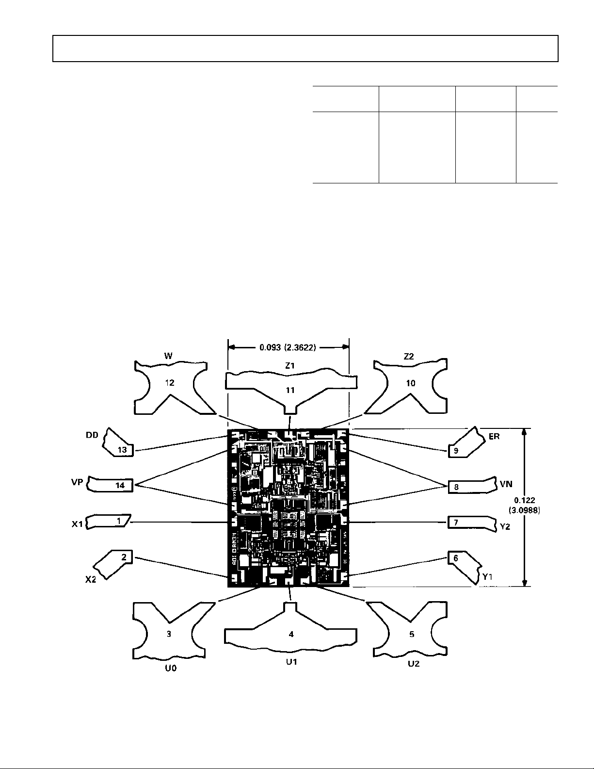
CHIP DIMENSIONS & BONDING DIAGRAM
Dimensions shown in inches and (mm).
(Contact factory for latest dimensions.)
ORDERING GUIDE
Temperature Package Package
Model Range Description Option
AD734AN –40°C to +85°C Plastic DIP N-14
AD734BN –40°C to +85°C Plastic DIP N-14
AD734AQ –40°C to +85°C Cerdip Q-14
AD734BQ –40°C to +85°C Cerdip Q-14
AD734SQ/883B –55°C to +125°C Cerdip Q-14
AD734SCHIPS –55°C to +125°CDie
REV. C
–3–
Page 4
AD734
W = A
O
X
1
− X
2
()
Y
1−Y2
()
U
− Z1− Z
2
()
W =
X
1
− X
2
()
Y
1−Y2
()
U
+ Z
2
.
X1
X2
U0
U1
Ru
U2
Y1
Y2
X = X1 – X
XIF
DD
DENOMINATOR
CONTROL
ER
YIF
Y = Y1 – Y
XZ
U
HIGH-ACCURACY
TRANSLINER
MULTIPLIER CORE
∑
Z = Z1 – Z
XY/U – Z
WIF
A
AD734
2
W
O
∞
ZIF
Z1
Z2
2
U
2
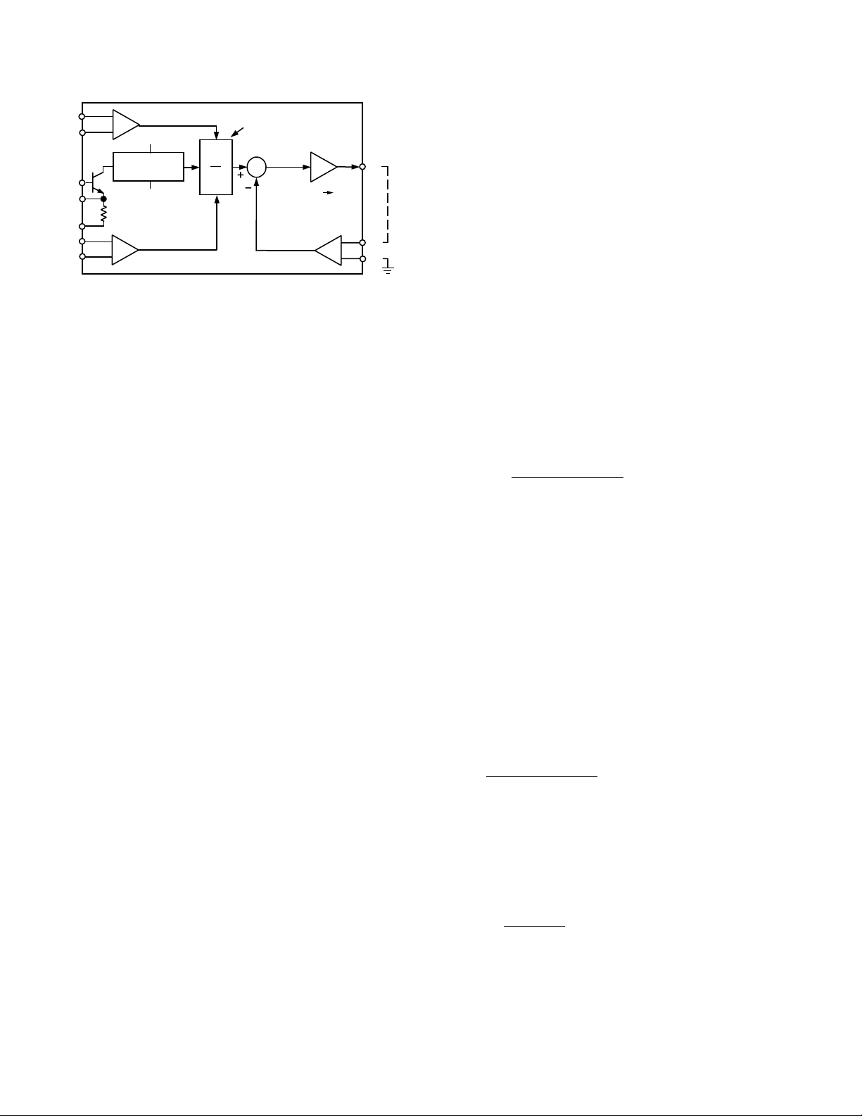
Figure 1. AD734 Block Diagram
FUNCTIONAL DESCRIPTION
Figure 1 is a simplified block diagram of the AD734. Operation
is similar to that of the industry-standard AD534 and in many
applications these parts are pin-compatible. The main functional
difference is the provision for direct control of the denominator
voltage, U, explained fully on the following page. Internal signals are actually in the form of currents, but the function of the
AD734 can be understood using voltages throughout, as shown
in this figure. Pins are named using upper-case characters (such
as X1, Z2) while the voltages on these pins are denoted by subscripted variables (for example, X
, Z2).
1
The AD734’s differential X, Y and Z inputs are handled by
wideband interfaces that have low offset, low bias current and
low distortion. The AD734 responds to the difference signals
X = X
– X2, Y = Y1 – Y2 and Z = Z1 – Z2, and rejects
1
common-mode voltages on these inputs. The X, Y and Z
interfaces provide a nominal full-scale (FS) voltage of ±10 V,
but, due to the special design of the input stages, the linear
range of the differential input can be as large as ±17 V. Also
unlike previous designs, the response on these inputs is not
clipped abruptly above ±15 V, but drops to a slope of one half.
The bipolar input signals X and Y are multiplied in a translinear
core of novel design to generate the product XY/U. The
denominator voltage, U, is internally set to an accurate,
temperature-stable value of 10 V, derived from a buried-Zener
reference. An uncalibrated fraction of the denominator voltage
U appears between the voltage reference pin (ER) and the
negative supply pin (VN), for use in certain applications where
a temperature-compensated voltage reference is desirable. The
internal denom-inator, U, can be disabled, by connecting the
denominator disable Pin 13 (DD) to the positive supply pin
(VP); the denom-inator can then be replaced by a fixed or
variable external volt-age ranging from 10 mV to more than 10 V.
The high-gain output op-amp nulls the difference between
XY/U and an additional signal Z, to generate the final output
W. The actual transfer function can take on several forms, depending on the connections used. The AD734 can perform all
of the functions supported by the AD534, and new functions
using the direct-division mode provided by the U-interface.
Each input pair (X1 and X2, Y1 and Y2, Z1 and Z2) has a
differential input resistance of 50 kΩ; this is formed by “real”
resistors (not a small-signal approximation) and is subject to a
tolerance of ±20%. The common-mode input resistance is
several megohms and the parasitic capacitance is about 2 pF.
The bias currents associated with these inputs are nulled by
laser-trimming, such that when one input of a pair is optionally
ac-coupled and the other is grounded, the residual offset voltage
is typically less than 5 mV, which corresponds to a bias current
of only 100 nA. This low bias current ensures that mismatches
in the sources resistances at a pair of inputs does not cause an
offset error. These currents remain low over the full temperature
range and supply voltages.
The common-mode range of the X, Y and Z inputs does not
fully extend to the supply rails. Nevertheless, it is often possible
to operate the AD734 with one terminal of an input pair connected to either the positive or negative supply, unlike previous
multipliers. The common-mode resistance is several megohms.
The full-scale output of ±10 V can be delivered to a load resistance of 1 kΩ (although the specifications apply to the standard
multiplier load condition of 2 kΩ). The output amplifier is
stable driving capacitive loads of at least 100 pF, when a slight
increase in bandwidth results from the peaking caused by this
capacitance. The 450 V/µs slew rate of the AD734’s output am-
plifier ensures that the bandwidth of 10 MHz can be maintained
up to the full output of 20 V pk-pk. Operation at reduced supply
voltages is possible, down to ±8 V, with reduced signal levels.
Available Transfer Functions
The uncommitted (open-loop) transfer function of the AD734 is
, (1)
where A
is the open-loop gain of the output op-amp, typically
O
72 dB. When a negative feedback path is provided, the circuit
will force the quantity inside the brackets essentially to zero,
resulting in the equation
(X
– X2)(Y1 – Y2) = U (Z1 – Z2) (2)
1
This is the most useful generalized transfer function for the
AD734; it expresses a balance between the product XY and the
product UZ. The absence of the output, W, in this equation
only reflects the fact that we have not yet specified which of the
inputs is to be connected to the op amp output.
Most of the functions of the AD734 (including division, unlike
the AD534 in this respect) are realized with Z
So, substituting W in place of Z
in the above equation results in
1
connected to W.
1
an output.
(3)
The free input Z2 can be used to sum another signal to the
output; in the absence of a product signal, W simply follows the
voltage at Z2 with the full 10 MHz bandwidth. When not
needed for summation, Z2 should be connected to the ground
associated with the load circuit. We can show the allowable
polarities in the following shorthand form:
±X
±Y
()
±W
=
()
()
+U
()
+±Z.
(4)
In the recommended direct divider mode, the Y input is set to a
fixed voltage (typically 10 V) and U is varied directly; it may
have any value from 10 mV to 10 V. The magnitude of the ratio
X/U cannot exceed 1.25; for example, the peak X-input for U
= 1 V is ±1.25 V. Above this level, clipping occurs at the
positive and negative extremities of the X-input. Alternatively,
–4–
REV. C
Page 5
AD734
the AD734 can be operated using the standard (AD534) divider
connections (Figure 8), when the negative feedback path is
established via the Y
input. Substituting W for Y2 in Equation
2
(2), we get
− Z
Z
()
2
W =U
()
1
+Y
.
X
− X
1
1
2
(5)
In this case, note that the variable X is now the denominator,
and the above restriction (X/U ≤ 1.25) on the magnitude of the
X input does not apply. However, X must be positive in order
for the feedback polarity to be correct. Y
can be used for
1
summing purposes or connected to the load ground if not
needed. The shorthand form in this case is
±Z
±W
=+U
()
()
()
+X
()
+±Y
.
()
(6)
In some cases, feedback may be connected to two of the available inputs. This is true for the square-rooting connections
(Fig-ure 9), where W is connected to both X
= W and Y2 = W in Equation (2), and anticipating the
X
1
possibility of again providing a summing input, so setting X
= S, we find, in shorthand form
and Y
1
±W
=+U
()
+Z
()
+±S
()
.
()
and Y2. Setting
1
= S
2
(7)
This is seen more generally to be the geometric-mean function,
since both U and Z can be variable; operation is restricted to
one quadrant. Feedback may also be taken to the U-interface.
Full details of the operation in these modes is provided in the
appropriate section of this data sheet.
Direct Denominator Control
A valuable new feature of the AD734 is the provision to replace
the internal denominator voltage, U, with any value from +10 mV
to +10 V. This can be used (1) to simply alter the multiplier
scaling, thus improve accuracy and achieve reduced noise levels
when operating with small input signals; (2) to implement an
accurate two-quadrant divider, with a 1000:1 gain range and an
asymptotic gain-bandwidth product of 200 MHz; (3) to achieve
certain other special functions, such as AGC or rms.
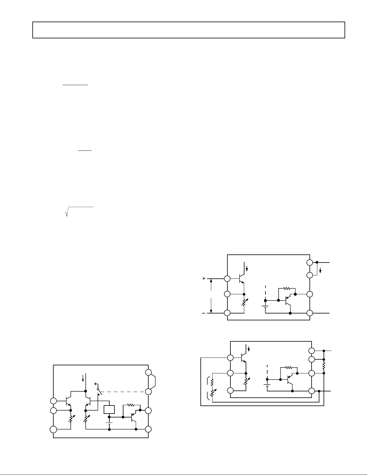
Figure 2 shows the internal circuitry associated with denominator control. Note first that the denominator is actually proportional
to a current, Iu, having a nominal value of 356 µA for U = 10 V,
whereas the primary reference is a voltage, generated by a buriedZener circuit and laser-trimmed to have a very low temperature
coefficient. This voltage is nominally 8 V with a tolerance of
±10%.
U0
U2
NOMINALLY
356mA for
Iu
U = 10V
3
U1
4
Ru
28kV
5
Qu
Qd
Rd
NOM
22.5kV
AD734
Rr
100kV
TC
NOM
8V
NEGATIVE SUPPLY
Qr
14
13
9
8
VP
LINK TO
DISABLE
DD
ER
VN
After temperature-correction (block TC), the reference voltage
is applied to transistor Qd and trimmed resistor Rd, which
generate the required reference current. Transistor Qu and
resistor Ru are not involved in setting up the internal denominator,
and their associated control pins U0, U1 and U2 will normally
be grounded. The reference voltage is also made available, via
the 100 kΩ resistor Rr, at Pin 9 (ER); the purpose of Qr is
explained below.
When the control pin DD (denominator disable) is connected to
VP, the internal source of Iu is shut off, and the collector current of Qu must provide the denominator current. The resistor
Ru is laser-trimmed such that the multiplier denominator is
exactly equal to the voltage across it (that is, across pins U1 and
U2). Note that this trimming only sets up the correct internal
ratio; the absolute value of Ru (nominally 28 kΩ) has a
tolerance of ±20%. Also, the alpha of Qu, (typically 0.995)
which might be seen as a source of scaling error, is canceled by
the alpha of other transistors in the complete circuit.
In the simplest scheme (Figure 3), an externally-provided
control voltage, V
resulting voltage across Ru is therefore reduced by one V
example, when V
, is applied directly to U0 and U2 and the
G
= 2 V, the actual value of U will be about
G
BE
. For
1.3 V. This error will not be important in some closed-loop
applications, such as automatic gain control (AGC), but clearly
is not acceptable where the denominator value must be welldefined. When it is required to set up an accurate, fixed value of
U, the on-chip reference may be used. The transistor Qr is
provided to cancel the V
of Qu, and is biased by an external
BE
resistor, R2, as shown in Figure 4. R1 is chosen to set the desired value of U and consists of a fixed and adjustable resistor.
NC
~
+V
60mA
–V
S
S
14
VP
Iu
U0
Qu
3
U1
4
V
NC
G
Ru
28kV
U2
5
AD734
Rr
100kV
13
DD
ER
9
Qr
VN
8
Figure 3. Low-Accuracy Denominator Control
Iu
Ru
28kV
AD734
NOM
8V
100kV
U0
Qu
3
U1
4
NC
U2
5
R1
VP
14
DD
ER
VN
13
9
8
Rr
Qr
+V
S
R2
–V
S
Figure 4. Connections for a Fixed Denominator
Table I shows useful values of the external components for setting up nonstandard denominator values.
REV. C
Figure 2. Denominator Control Circuitry
–5–
Page 6
1
2
3
4
5
6
7
10
8
9
11
13
12
14
W
ER
VN
VP
DD
Z1
Z2
X1
X2
U1
U2
U0
Y1
Y2
AD734
NC
NC
LOAD
GROUND
0.1
mF
0.1
mF
X – INPUT
610V FS
Y – INPUT
610V FS
+15V
–15V
OPTIONAL
SUMMING INPUT
±10V FS
W =
(X
1
– X2)
10V
(Y
1
– Y2)
+ Z
2
L
L
Z
2
1
2
3
4
5
6
7
10
8
9
11
13
1214W
ER
VN
VP
DD
Z1
Z2
X1
X2
U1
U2
U0
Y1
Y2
AD734
NC
NC
L
0.1mF
0.1mF
X – INPUT
610V FS
Y – INPUT
610V FS
+15V
–15V
I
W
=
(X1 – X2)
10V
(Y1 – Y2)
1
R
S
+
1
50kV
R
S
L
610mA MAX FS
610V MAXIMUM
LOAD VOLTAGE
L
LOAD
I
W
AD734
Table I. Component Values for Setting Up Nonstandard
Denominator Values
Denominator R1 (Fixed) R1 (Variable) R2
5 V 34.8 kΩ 20 kΩ 120 kΩ
3 V 64.9 kΩ 20 kΩ 220 kΩ
2 V 86.6 kΩ 50 kΩ 300 kΩ
1 V 174 kΩ 100 kΩ 620 kΩ
The denominator can also be current controlled, by grounding
Pin 3 (U0) and withdrawing a current of Iu from Pin 4 (U1).
The nominal scaling relationship is U = 28 × Iu, where u is
expressed in volts and Iu is expressed in milliamps. Note,
however, that while the linearity of this relationship is very good,
it is subject to a scale tolerance of ±20%. Note that the common
mode range on Pins 3 through 5 actually extends from 4 V to
36 V below VP, so it is not necessary to restrict the connection
of U0 to ground if it should be desirable to use some other
voltage.
The output ER may also be buffered, re-scaled and used as a
general-purpose reference voltage. It is generated with respect to
the negative supply line Pin 8 (VN), but this is acceptable when
driving one of the signal interfaces. An example is shown in
Figure 12, where a fixed numerator of 10 V is generated for a
divider application. There, Y
this; therefore the common-mode voltage at this interface is still
5 V above VN, which satisfies the internal biasing requirements
(see Specifications table).
OPERATION AS A MULTIPLIER
All of the connection schemes used in this section are essentially
identical to those used for the AD534, with which the AD734 is
pin-compatible. The only precaution to be noted in this regard
is that in the AD534, Pins 3, 5, 9, and 13 are not internally
connected and Pin 4 has a slightly different purpose. In many
cases, an AD734 can be directly substituted for an AD534 with
immediate benefits in static accuracy, distortion, feedthrough,
and speed. Where Pin 4 was used in an AD534 application to
achieve a reduced denominator voltage, this function can now be
much more precisely implemented with the AD734 using alter-
native connections (see Direct Denominator Control, page 5).
Operation from supplies down to ±8 V is possible. The supply
current is essentially independent of voltage. As is true of all
high speed circuits, careful power-supply decoupling is impor-
tant in maintaining stability under all conditions of use. The
decoupling capacitors should always be connected to the load
ground, since the load current circulates in these capacitors at
high frequencies. Note the use of the special symbol (a triangle
with the letter ‘L’ inside it) to denote the load ground.
Standard Multiplier Connections
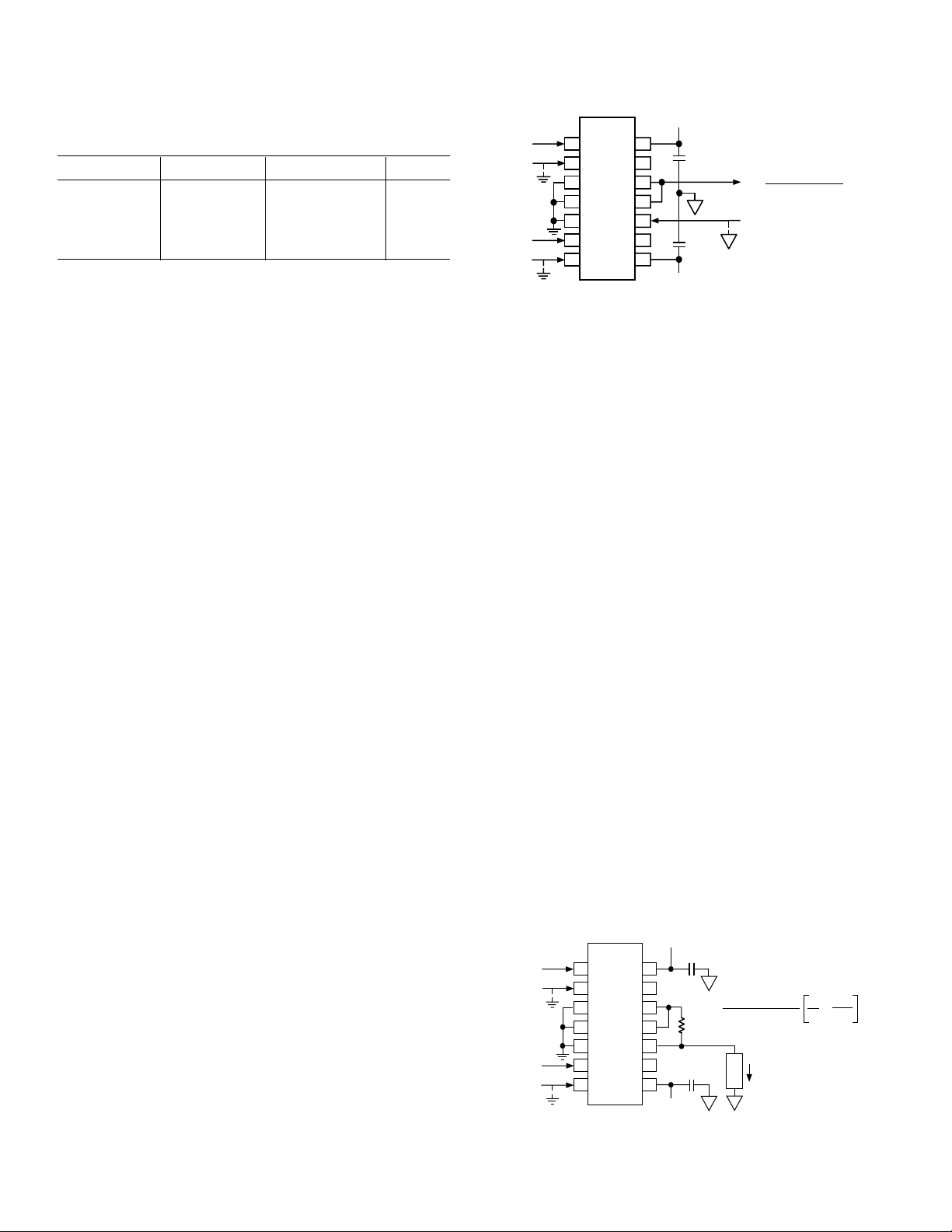
Figure 5 shows the basic connections for multiplication. The X
and Y inputs are shown as optionally having their negative
nodes grounded, but they are fully differential, and in many
applications the grounded inputs may be reversed (to facilitate
interfacing with signals of a particular polarity, while achieving
some desired output polarity) or both may be driven.
The AD734 has an input resistance of 50 kΩ ± 20% at the X,
Y, and Z interfaces, which allows ac-coupling to be achieved
with moderately good control of the high-pass (HP) corner
frequency; a capacitor of 0.1 µF provides a HP corner frequency
is tied to VN but Y1 is 10 V above
2
–6–
Figure 5. Basic Multiplier Circuit
of 32 Hz. When a tighter control of this frequency is needed, or
when the HP corner is above about 100 kHz, an external resistor should be added across the pair of input nodes.
At least one of the two inputs of any pair must be provided with
a dc path (usually to ground). The careful selection of ground
returns is important in realizing the full accuracy of the AD734.
The Z2 pin will normally be connected to the load ground,
which may be remote, in some cases. It may also be used as an
optional summing input (see Equations (3) and (4), above)
having a nominal FS input of ±10 V and the full 10 MHz
bandwidth.
In applications where high absolute accuracy is essential, the
scaling error caused by the finite resistance of the signal source(s)
may be troublesome; for example, a 50 Ω source resistance at
just one input will introduce a gain error of –0.1%; if both the
X- and Y-inputs are driven from 50 Ω sources, the scaling error
in the product will be –0.2%. Provided the source resistance(s)
are known, this gain error can be completely compensated by
including the appropriate resistance (50 Ω or 100 Ω, respectively,
in the above cases) between the output W (Pin 12) and the Z1
feedback input (Pin 11). If Rx is the total source resistance
associated with the X1 and X2 inputs, and Ry is the total source
resistance associated with the Y1 and Y2 inputs, and neither Rx
nor Ry exceeds 1 kΩ, a resistance of Rx+Ry in series with pin
Z1 will provide the required gain restoration.
Pins 9 (ER) and 13 (DD) should be left unconnected in this
application. The U-inputs (Pins 3, 4 and 5) are shown
connected to ground; they may alternatively be connected to
VN, if desired. In applications where Pin 2 (X2) happens to be
driven with a high-amplitude, high-frequency signal, the
capacitive coupling to the denominator control circuitry via an
ungrounded Pin 3 can cause high-frequency distortion. However,
the AD734 can be operated without modification in an AD534
socket, and these three pins left unconnected, with the above
caution noted.
Figure 6. Conversion of Output to a Current
REV. C
Page 7
AD734
Z INPUT
610V FS
X INPUT
+0.1V TO
+10V
OPTIONAL
SUMMING
INPUT
610V FS
W = 10
+Y1
(Z
2
– Z1)
(X1 – X2)
1
2
3
4
5
6
7
10
8
9
11
13
12
14
W
ER
VN
VP
DD
Z1
Z2
X1
X2
U1
U2
U0
Y1
Y2
AD734
NC
NC
0.1mF
0.1
mF
+15V
–15V
L
L
Y
1
L
Current Output
It may occasionally be desirable to convert the output voltage to
a current. In correlation applications, for example, multiplication is followed by integration; if the output is in the form of a
current, a simple grounded capacitor can perform this function.
Figure 6 shows how this can be achieved. The op amp forces
the voltage across Z1 and Z2, and thus across the resistor R
, to
S
be the product XY/U. Note that the input resistance of the
Z interface is in shunt with R
, which must be calculated
S
accordingly.
The smallest FS current is simply ±10 V/50 kΩ, or ±200 µA,
with a tolerance of about 20%. To guarantee a 1% conversion
tolerance without adjustment, R
must be less than 2.5 kΩ. The
S
maximum full scale output current should be limited to about
±10 mA (thus, R
= 1 kΩ). This concept can be applied to all
S
connection modes, with the appropriate choice of terminals.
Squaring and Frequency-Doubling
Squaring of an input signal, E, is achieved simply by connecting
the X and Y inputs in parallel; the phasing can be chosen to
produce an output of E
2
/U or –E2/U as desired. The input may
have either polarity, but the basic output will either always be
positive or negative; as for multiplication, the Z2 input may be
used to add a further signal to the output.
When the input is a sine wave, a squarer behaves as a frequencydoubler, since
(Esinwt)
2
= E2 (1 – cos2wt)/2 (8)
Equation (8) shows a dc term at the output which will vary
strongly with the amplitude of the input, E. This dc term can be
avoided using the connection shown in Figure 7, where an
RC-network is used to generate two signals whose product has
no dc term. The output is
VP
DD
ER
VN
+15V
0.1mF
14
13
NC
W
12
Z1
11
10
Z2
9
NC
8
–15V
0.1mF
L
L
R3
13kV
R4
4.32kV
L
E cos2ωt2/10V
Esinωt
1.6kV
R1
R2
1
2
3
4
5
6
7
AD734
X1
X2
U0
U1
U2
Y1
Y2
1.6kV
C
Figure 7. Frequency Doubler
OPERATION AS A DIVIDER
The AD734 supports two methods for performing analog
division. The first is based on the use of a multiplier in a feedback loop. This is the standard mode recommended for
multipliers having a fixed scaling voltage, such as the AD534,
and will be described in this Section. The second uses the
AD734’s unique capability for externally varying the scaling
(denominator) voltage directly, and will be described in the
next section.
Feedback Divider Connections
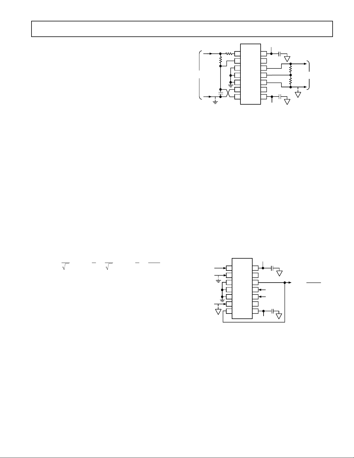
Figure 8 shows the connections for the standard (AD534)
divider mode. Feedback from the output, W, is now taken to the
Y2 (inverting) input, which, provided that the X-input is positive, establishes a negative feedback path. Y1 should normally
be connected to the ground associated with the load circuit, but
may optionally be used to sum a further signal to the output. If
desired, the polarity of the Y-input connections can be reversed,
with W connected to Y1 and Y2 used as the optional summation
input. In this case, either the polarity of the X-input connections
must be reversed, or the X-input voltage must be negative.
W = 4
E
sin wt +
2
π
4
E
sin wt −
2
π
1
4
10 V
for w = 1/CR1, which is just
2
W = E
(cos2wt)/( 10 V) (10)
which has no dc component. To restore the output to ±10 V
when E = 10 V, a feedback attenuator with an approximate ratio
of 4 is used between W and Z1; this technique can be used
wherever it is desired to achieve a higher overall gain in the
transfer function.
In fact, the values of R3 and R4 include additional compensa-
tion for the effects of the 50 kΩ input resistance of all three
interfaces; R2 is included for a similar reason. These resistor
values should not be altered without careful calculation of the
consequences; with the values shown, the center frequency f
100 kHz for C = 1 nF. The amplitude of the output is only a
weak function of frequency: the output amplitude will be 0.5%
too low at f = 0.9f
and f = 1.1f0. The cross-connection is simply
0
to produce the cosine output with the sign shown in Equation
(10); however, the sign in this case will rarely be important.
REV. C
(9)
Figure 8. Standard (AD534) Divider Connection
The numerator input, which is differential and can have either
polarity, is applied to pins Z1 and Z2. As with all dividers based
is
0
on feedback, the bandwidth is directly proportional to the
denominator, being 10 MHz for X = 10 V and reducing to
100 kHz for X = 100 mV. This reduction in bandwidth, and the
increase in output noise (which is inversely proportional to the
denominator voltage) preclude operation much below a denominator of 100 mV. Division using direct control of the denominator
(Figure 10) does not have these shortcomings.
–7–
Page 8
AD734
100kV
SCALE
ADJUST
200kV
10V
W =
(X1– X2)
+ Z
2
U1–U
2
OP AMP = AD712 DUAL
2MV
X – INPUT
U – INPUT
1
2
3
4
5
6
7
10
8
9
11
13
12
14
W
ER
VN
VP
DD
Z1
Z2
X1
X2
U1
U2
U0
Y1
Y2
AD734
L
LOAD
GROUND
0.1mF
0.1mF
+15V
–15V
OPTIONAL
SUMMING
INPUT
610V FS
L
Z
2
U
1
U
2
VP
DD
ER
VN
+15V
0.1mF
14
13
W
12
Z1
11
10
Z2
9
8
NC
NC
–15V
L
D
Z INPUT
+10mV TO
+10V
0.1mF
(10V)W = (Z2 – Z1)+ S
L
OPTIONAL
SUMMING
INPUT
610V FS
AD734
1
X1
2
X2
3
U0
4
S
L
U1
5
U2
6
Y1
7
Y2
Figure 9. Connection for Square Rooting
Connections for Square-Rooting
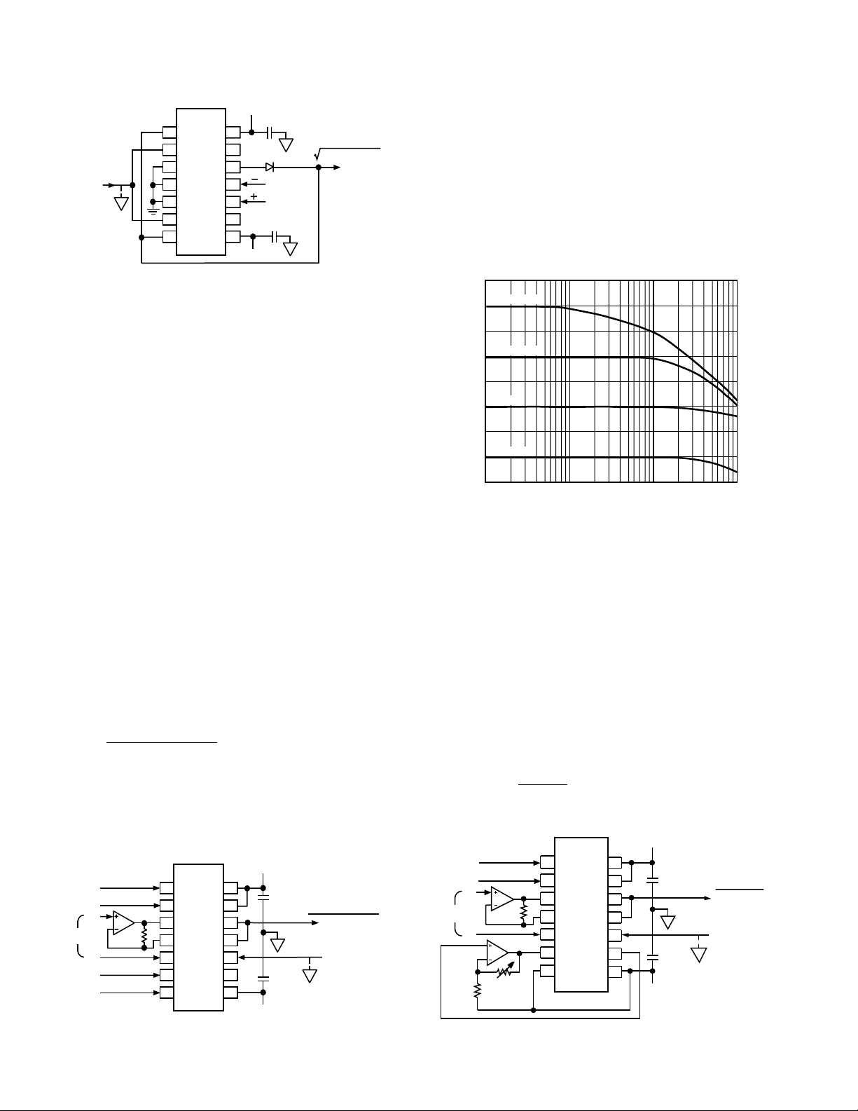
The AD734 may be used to generate an output proportional to
the square-root of an input using the connections shown in
Figure 9. Feedback is now via both the X and Y inputs, and is
always negative because of the reversed-polarity between these
two inputs. The Z input must have the polarity shown, but
because it is applied to a differential port, either polarity of
input can be accepted with reversal of Z1 and Z2, if necessary.
The diode D, which can be any small-signal type (1N4148
being suitable) is included to prevent a latching condition which
could occur if the input momentarily was of the incorrect
polarity of the input, the output will be always negative.
Note that the loading on the output side of the diode will be
provided by the 25 kΩ of input resistance at X1 and Y2, and by
the user’s load. In high speed applications it may be beneficial
to include further loading at the output (to 1 kΩ minimum) to
speed up response time. As in previous applications, a further
signal, shown here as S, may be summed to the output; if this
option is not used, this node should be connected to the load
ground.
DIVISION BY DIRECT DENOMINATOR CONTROL
The AD734 may be used as an analog divider by directly varying the denominator voltage. In addition to providing much
higher accuracy and bandwidth, this mode also provides greater
flexibility, because all inputs remain available. Figure 10 shows
the connections for the general case of a three-input multiplier
divider, providing the function
X
− X
()
W =
1
Y
()
2
1−Y2
U
()
1−U2
+ Z
2,
(11)
where the X, Y, and Z signals may all be positive or negative,
but the difference U = U
– U2 must be positive and in the
1
range +10 mV to +10 V. If a negative denominator voltage must
be used, simply ground the noninverting input of the op amp.
As previously noted, the X input must have a magnitude of less
than 1.25U.
AD734
1
2
3
4
5
6
7
X – INPUT
U
1
U – INPUT
Y – INPUT
Figure 10. Three-Variable Multiplier/Divider Using Direct
Denominator Control
2MV
U
2
VP
X1
DD
X2
W
U0
Z1
U1
Z2
U2
ER
Y1
VN
Y2
+15V
14
13
12
11
10
9
8
0.1mF
L
NC
0.1mF
–15V
(X
W =
LOAD
GROUND
L
(Y1 – Y2)
– X2)
1
U1 – U
2
Z
2
OPTIONAL
SUMMING INPUT
610V FS
+ Z
This connection scheme may also be viewed as a variable-gain
element, whose output, in response to a signal at the X input, is
controllable by both the Y input (for attenuation, using Y less
than U) and the U input (for amplification, using U less than
Y). The ac performance is shown in Figure 11; for these results,
Y was maintained at a constant 10 V. At U = 10 V, the gain is
unity and the circuit bandwidth is a full 10 MHz. At U = 1 V,
the gain is 20 dB and the bandwidth is essentially unaltered. At
U = 100 mV, the gain is 40 dB and the bandwidth is 2 MHz.
Finally, at U = 10 mV, the gain is 60 dB and the bandwidth is
250 kHz, corresponding to a 250 MHz gain-bandwidth product.
70
U = 10mV
60
50
U = 100mV
40
30
GAIN – dB
U = 1V
20
10
U = 10V
0
10k 100k 1M 10M
FREQUENCY – Hz
Figure 11. Three-Variable Multiplier/Divider Performance
The 2 MΩ resistor is included to improve the accuracy of the
gain for small denominator voltages. At high gains, the X input
offset voltage can cause a significant output offset voltage. To
eliminate this problem, a low-pass feedback path can be used
from W to X2; see Figure 13 for details.
Where a numerator of 10 V is needed, to implement a twoquadrant divider with fixed scaling, the connections shown in
Figure 12 may be used. The reference voltage output appearing
between Pin 9 (ER) and Pin 8 (VN) is amplified and buffered
by the second op amp, to impose 10 V across the Y1/Y2 input.
Note that Y2 is connected to the negative supply in this application. This is permissible because the common-mode voltage is
still high enough to meet the internal requirements. The transfer
function is
W =10 V
X
U
− X
1
1−U2
2
+ Z
.
2
The ac performance of this circuit remains as shown in Figure 11.
2
Figure 12. Two-Quadrant Divider with Fixed 10 V Scaling
–8–
(12)
REV. C
Page 9
AD734
+2
+1
0
–1
–2
ERROR – dB
10m 100m 1 10
INPUT AMPLITUDE – Volts
100kHZ
100HZ
1MHZ
L
1/2
AD708
V
IN
2
VO =
V
O
R1
3.32kV
V
IN
1
2
3
4
5
6
7
10
8
9
11
13
12
14
W
ER
VN
VP
DD
Z1
Z2
X1
X2
U1
U2
U0
Y1
Y2
AD734
0.1mF
0.1mF
+15V
–15V
U2a
C1
47mF
U1
L
L
L
C2
1mF
L
L
L
1/2
AD708
U2b
A PRECISION AGC LOOP
The variable denominator of the AD734 and its high gainbandwidth product make it an excellent choice for precise
automatic gain control (AGC) applications. Figure 13 shows a
suggested method. The input signal, E
peak amplitude of from 10 mV to 10 V at any frequency from
100 Hz to 10 MHz, is applied to the X input, and a fixed positive voltage E
to the Y input. Op amp A2 and capacitor C2
C
form an integrator having a current summing node at its inverting input. (The AD712 dual op amp is a suitable choice for this
application.) In the absence of an input, the current in D2 and
R2 causes the integrator output to ramp negative, clamped by
diode D3, which is included to reduce the time required for the
loop to establish a stable, calibrated, output level once the
circuit has received an input signal. With no input to the
denominator (U0 and U2), the gain of the AD734 is very high
(about 70 dB), and thus even a small input causes a substantial
output.
R3
NC
1MV
AD734
X1
1
2
X2
U0
3
4
U1
U2
5
6
Y1
Y2
7
E
1N914
+1V TO
+10V
C1
C2
1mF
D2
1N914
R2
1MVR11MV
A1
A2
1mF
IN
D3
E
C
Figure 13. Precision AGC Loop
Diode D1 and C1 form a peak detector, which rectifies the output and causes the integrator to ramp positive. When the
current in R1 balances the current in R2, the integrator output
holds the denominator output at a constant value. This occurs
when there is sufficient gain to raise the amplitude of E
required to establish an output amplitude of E
of +1 V to +10 V. The X input of the AD734, which has finite
offset voltage, could be troublesome at the output at high gains.
The output offset is reduced to that of the X input (one or two
millivolts) by the offset loop comprising R3, C3, and buffer A1.
The low pass corner frequency of 0.16 Hz is transformed to a
high-pass corner that is multiplied by the gain (for example,
160 Hz at a gain of 1000).
In applications not requiring operation down to low frequencies,
amplifier A1 can he eliminated, but the AD734’s input
resistance of 50 kΩ between X1 and X2 will reduce the time
constant and increase the input offset. Using a non-polar 20 µF
tantalum capacitor for C1 will result in the same unity-gain
high-pass corner; in this case, the offset gain increases to 20, still
very acceptable.
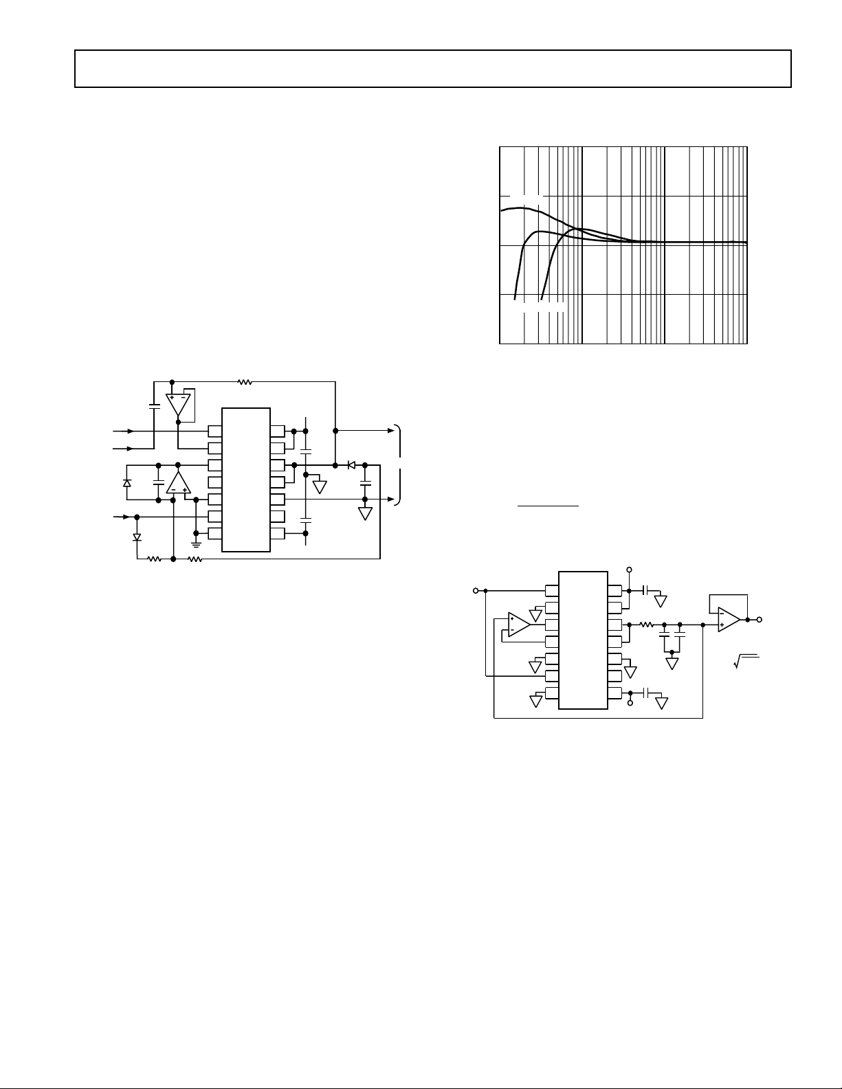
Figure 14 shows the error in the output for sinusoidal inputs at
100 Hz, 100 kHz, and 1 MHz, with E
put error for any frequency between 300 Hz and 300 kHz is
similar to that for 100 kHz. At low signal frequencies and low
input amplitudes, the dynamics of the control loop determine
the gain error and distortion; at high frequencies, the 200 MHz
gain-bandwidth product of the AD734 limit the available gain.
REV. C
, which may have a
IN
+15V
14
VP
DD
W
Z1
Z2
ER
VN
0.1mF
13
12
11
10
9
8
–15V
set to +10 V. The out-
C
D1
1N914
C1
L
1mF
0.1mF
OP AMP = AD712 DUAL
over the range
C
L
IN
E
OUT
to that
The output amplitude tracks E
over the range +1 V to slightly
C
more than +10 V.
Figure 14. AGC Amplifier Output Error vs. Input Voltage
WIDEBAND RMS-DC CONVERTER
USING U INTERFACE
The AD734 is well suited to such applications as implicit RMSDC conversion, where the AD734 implements the function
avg V
V
=
RMS
2
IN
[]
V
RMS
using its direct divide mode. Figure 15 shows the circuit.
Figure 15. A 2-Chip, Wideband RMS-DC Converter
In this application, the AD734 and an AD708 dual op amp
serve as a 2-chip RMS-DC converter with a 10 MHz bandwidth.
Figure 16 shows the circuit’s performance for square-, sine-,
and triangle-wave inputs. The circuit accepts signals as high as
10 V p-p with a crest factor of 1 or 1 V p-p with a crest factor of
10. The circuit’s response is flat to 10 MHz with an input of
10 V, flat to almost 5 MHz for an input of 1 V, and to almost
1 MHz for inputs of 100 mV. For accurate measurements of
input levels below 100 mV, the AD734’s output offset (Z interface) voltage, which contributes a dc error, must be trimmed out.
In Figure 15’s circuit, the AD734 squares the input signal, and
its output (V
2
) is averaged by a low-pass filter that consists of
IN
R1 and C1 and has a corner frequency of 1 Hz. Because of the
implicit feedback loop, this value is both the output value, V
and the denominator in Equation (13). U2a and U2b, an
AD708 dual dc precision op amp, serve as unity-gain buffers,
supplying both the output voltage and driving the U interface.
–9–
(13)
RMS
,
Page 10
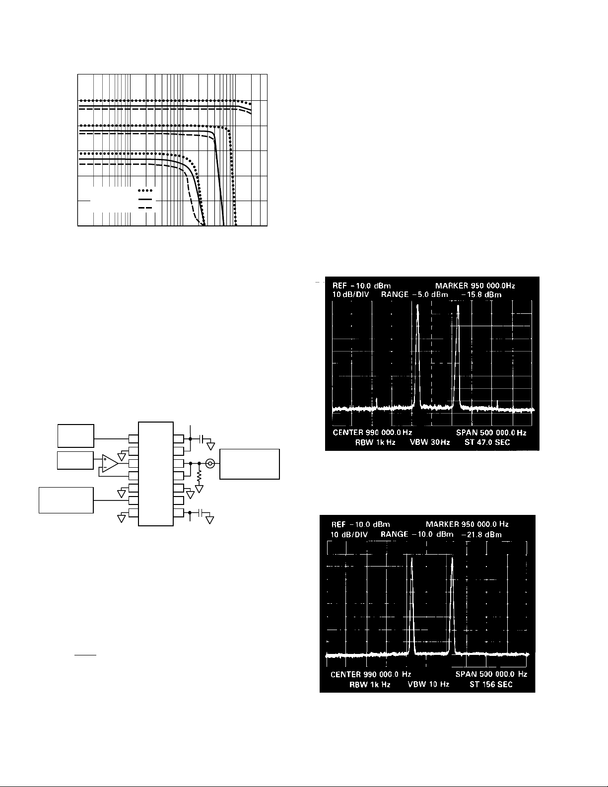
AD734
100
10
1
100m
10m
OUTPUT VOLTAGE – Volts
SQUARE WAVE
SINE WAVE
1m
TRI-WAVE
100m
10k 100k 1M 10M
INPUT FREQUENCY – Hz
Figure 16. RMS-DC Converter Performance
LOW DISTORTION MIXER
The AD734’s low noise and distortion make it especially
suitable for use as a mixer, modulator, or demodulator.
Although the AD734’s –3 dB bandwidth is typically 10 MHz
and is established by the output amplifier, the bandwidth of its
X and Y interfaces and the multiplier core are typically in excess
of 40 MHz. Thus, provided that the desired output signal is less
than 10 MHz, as would typically be the case in demodulation,
the AD734 can be used with both its X and Y input signals as
high as 40 MHz. One test of mixer performance is to linearly
combine two closely spaced, equal-amplitude sinusoidal signals
and then mix them with a third signal to determine the mixer’s
2-tone Third-Order Intermodulation Products.
VP
DD
ER
VN
+15V
0.1mF
14
13
12
W
Z1
Z2
2kV
11
10
9
0.1mF
8
–
HP3585A
WITH 10X PROBE
dBm REF TO 50V
HP3326A
COMBINE
A + B
DATEL
DVC-8500
HP3326A
HIGH VOLTAGE
OPTION
AD707
1
2
3
4
5
6
7
AD734
X1
X2
U0
U1
U2
Y1
Y2
Figure 17. AD734 Mixer Test Circuit
Figure 17 shows a test circuit for measuring the AD734’s performance in this regard. In this test, two signals, at 10.05 MHz and
9.95 MHz are summed and applied to the AD734’s X interface.
A second 9 MHz signal is applied to the AD734’s Y interface.
The voltage at the U interface is set to 2 V to use the full
dynamic range of the AD734. That is, by connecting the W and
Z1 pins together, grounding the Y2 and X2 pins, and setting
U = 2 V, the overall transfer function is
If the two X1 inputs are at frequencies f
frequency at the Y1 input is f
, then the two-tone third-order
0
intermodulation products should appear at frequencies 2f
and 2f2 – f
f
0
the AD734 with f
9.00 MHz for a signal level of f
+24 dBm in Figure 18 and f
± f
. Figures 18 and 19 show the output spectra of
1
0
= 9.95 MHz, f2 = 10.05 MHz, and f0 =
1
& f2 of 6 dBm and f0 of
1
& f2 of 0 dBm and f0 of +24 dBm
1
and f2 and the
1
1
– f
±
2
in Figure 19. This performance is without external trimming of
the AD734’s X and Y input-offset voltages.
The possible Two Tone Intermodulation Products are at 2 ×
9.95 MHz – 10.05 MHz ± 9.00 MHz and 2 × 10.05 –
9.95 MHz ± 9.00 MHz; of these only the third-order products
at 0.850 MHz and 1.150 MHz are within the 10 MHz bandwidth of the AD734; the desired output signals are at
0.950 MHz and 1.050 MHz. Note that the difference (Figure
18) between the desired outputs and third-order products is
approximately 78 dB, which corresponds to a computed
third-order intercept point of +46 dBm.
Figure 18. AD734 Third-Order Intermodulation Performance
for f
= 9.95 MHz, f2 = 10.05 MHz, and f0 = 9.00 MHz and for
1
Signal Levels of f
& f2 of 6 dBm and f0 of +24 dBm. All Dis-
1
played Signal Levels Are Attenuated 20 dB by the 10X Probe
Used to Measure the Mixer’s Output
X
2 V
1Y1
(14)
W =
and W can be as high as 20 V p-p when X1 = 2 V p-p and Y1 =
10 V p-p. The 2 V p-p signal level corresponds to +10 dBm into
a 50 Ω input termination resistor connected from X1 or Y1 to
ground.
–10–
Figure 19. AD734 Third-Order Intermodulation Performance
for f
= 9.95 MHz, f2 = 10.05 MHz, and f0 = 9.00 MHz and for
1
Signal Levels of f
& f2 of 0 dBm and f0 of +24 dBm. All Dis-
1
played Signal Levels Are Attenuated 20 dB by the 10X Probe
Used to Measure the Mixer’s Output
REV. C
Page 11
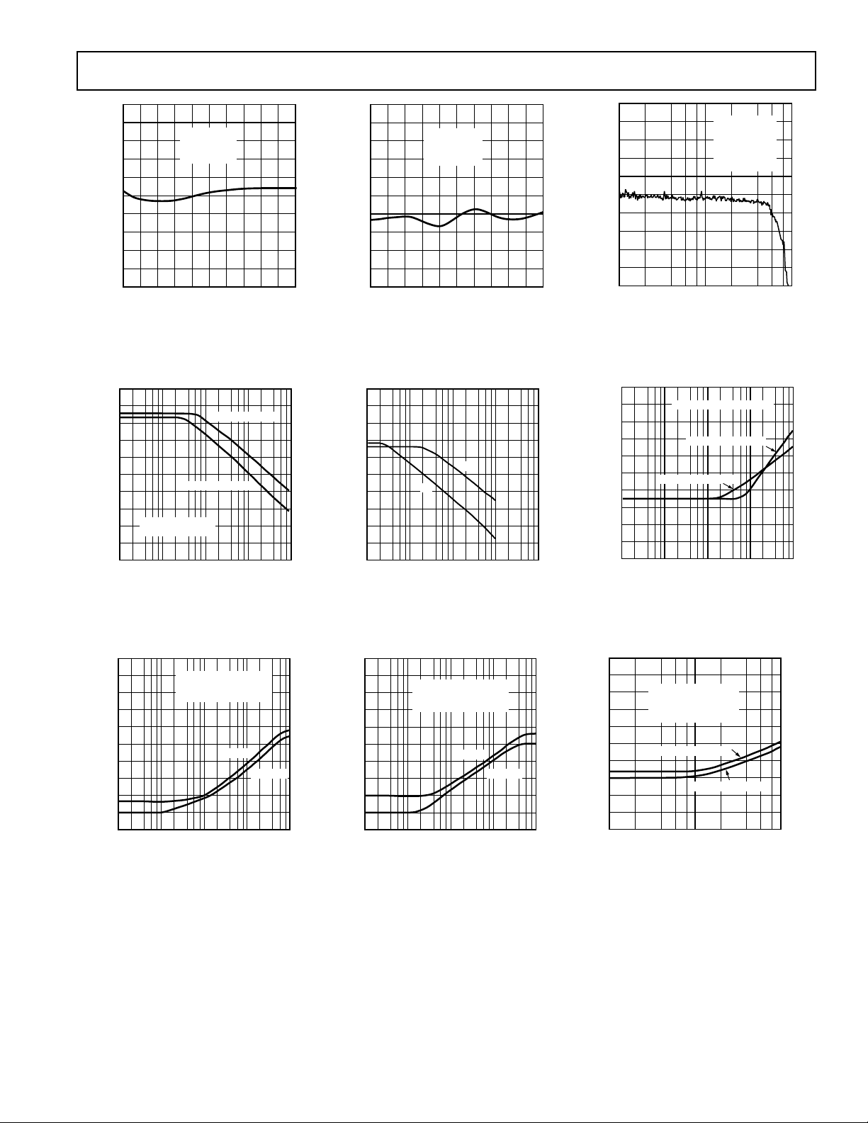
FREQUENCY – Hz
GAIN FLATNESS
100k 1M 10M
0.3
0.2
0.1
0
–0.1
–0.2
–0.3
–0.4
VS = 615V
X = 1.4V RMS
Y = 10V
R
LOAD
= 500V
C
LOAD
= 20pF
FEEDTHROUGH – dBc
FREQUENCY – Hz
0
–40
–60
–80
–100
1k 10k 10M100k 1M
Y INPUT, X NULLED
INPUT SIGNAL = 7V RMS
X INPUT, Y NULLED
SIGNAL LEVEL
dBc
0
–100
–10dBm
70.7mV RMS
–20
–40
–60
–80
10dBm
707mV RMS
30dBm
7V RMS
FREQUENCY = 1MHz
VP = 15V
VN = –15V
R
LOAD
= 2kV
Y INPUT. X = 10V DC
X INPUT. Y = 10V DC
Typical Characteristics–
AD734
0.06
0.04
0.02
0
–0.02
–0.04
DIFFERENTIAL GAIN – dB
–0.06
–0.08
–2V 2V
VS = 615V
R
= 2kV
LOAD
C
= 20pF
LOAD
0
SIGNAL AMPLITUDE
Figure 20. Differential Gain at
3.58 MHz and R
100
80
60
dB
40
COMMON-MODE
20
SIGNAL = 7V RMS
= 2 k
Ω
L
Y INPUT, X = 10V
X INPUT, Y = 10V
VS = 615V
R
= 2kV
LOAD
C
= 20pF
LOAD
0.1
0.05
0
–0.05
–0.1
DIFFERENTIAL PHASE – Degrees
–2V 2V
0
SIGNAL AMPLITUDE
Figure 21. Differential Phase at
3.58 MHz and R
100
80
60
40
PSRR – dB
20
= 2 k
Ω
L
VN
VP
Figure 22. Gain Flatness, 300 kHz to
10 MHz, R
= 500
L
Ω
0
1k 10k 10M100k 1M
FREQUENCY – Hz
Figure 23. CMRR vs. Frequency
0
–20
–40
dBc
–60
–80
1k 10k 10M100k 1M
FREQUENCY – Hz
Figure 26. THD vs. Frequency,
U = 2 V
REV. C
TEST INPUT = 1V RMS
U = 2V
OTHER INPUT = 2V DC
X INPUT
Y INPUT
0
1k 10k 10M100k 1M
FREQUENCY – Hz
Figure 24. PSRR vs. Frequency
0
–20
–40
dBc
–60
–80
1k 10k 10M100k 1M
TEST INPUT = 7V RMS
OTHER INPUT = 10V DC
= $2kV
R
LOAD
X INPUT
Y INPUT
FREQUENCY – Hz
Figure 27. THD vs. Frequency,
U = 10 V
–11–
Figure 25. Feedthrough vs. Frequency
Figure 28. THD vs. Signal Level,
f = 1 MHz
Page 12
AD734–Typical Characteristics
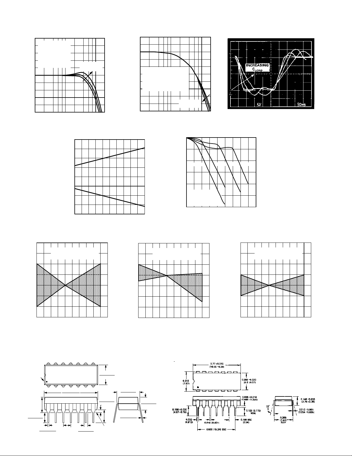
Y1 FREQUENCY – MHz
OUTPUT AMPLITUDE – dB
10 1006020 30 40 50 70 80 90
–30
–20
0
–10
X1 FREQ =
Y1 FREQ –1MHz
(
E.G., Y
1
– X1 = 1MHz
FOR ALL CURVES)
U = 1V
U = 2V
U = 5V
U = 10V
5
VS = 615V
4
X = 1.4V rms
Y = 10V
3
R
= 500V
LOAD
C
2
1
0
–1
AMPLITUDE – dB
–2
–3
–4
–5
100k 1M
Figure 29. Gain vs. Frequency vs.
C
LOAD
20
15
10
= 20pF, 47pF,
LOAD
100pF
FREQUENCY – Hz
20
15
10
–5
–10
OUTPUT SWING – Volts
–15
–20
Figure 32. Output Swing vs. Supply
Voltage
INPUT OFFSET VOLTAGE
DRIFT WILL TYPICALLY BE
WITHIN SHADED AREA
INCREASING
C
LOAD
10M
5
0
9101112 14151617
818
SUPPLY VOLTAGE – 6V
13
0
–30
–60
VS = 615V
X = 1.4V rms
–90
Y = 10V
–120
R
= 500V
LOAD
= 20pF, 47pF, 100pF
C
LOAD
–150
PHASE SHIFT – Degrees
–180
100k 1M 10M
FREQUENCY – Hz
INCREASING
C
LOAD
Figure 30. Phase vs. Frequency
vs. C
LOAD
S
Figure 33. Output Amplitude vs. Input
Frequency, When Used as Demodulator
60
INPUT OFFSET VOLTAGE
40
20
DRIFT WILL TYPICALLY BE
WITHIN SHADED AREA
Figure 31. Pulse Response vs.
C
, C
LOAD
= 0 pF, 47 pF,
LOAD
100 pF, 200 pF
8
INPUT OFFSET VOLTAGE
6
4
DRIFT WILL TYPICALLY BE
WITHIN SHADED AREA
C1442a–0–10/99
5
0
–5
DEVIATION OF INPUT
OFFSET VOLTAGE – mV
–10
–15
–15 5 25 45 65 85 105 125
–55 –35
TEMPERATURE – 8C
Figure 34. VOS Drift, X Input
0.160 (4.06)
0.115 (2.93)
14
PIN 1
1
0.210
(5.33)
MAX
0.022 (0.558)
0.014 (0.356)
0.795 (20.19)
0.725 (18.42)
0.100
(2.54)
BSC
0.070 (1.77)
0.045 (1.15)
8
7
0.280 (7.11)
0.240 (6.10)
0.060 (1.52)
0.015 (0.38)
0.130
(3.30)
MIN
SEATING
PLANE
0
–20
–40
DEVIATION OF INPUT
OFFSET VOLTAGE – mV
–60
–15 5 25 45 65 85 105 125
–55 –35
TEMPERATURE – 8C
Figure 35. VOS Drift, Z Input
OUTLINE DIMENSIONS
Dimensions shown in inches and (mm).
0.325 (8.25)
0.300 (7.62)
0.195 (4.95)
0.115 (2.93)
0.015 (0.381)
0.008 (0.204)
–12–
2
0
–2
DEVIATION OF INPUT
OFFSET VOLTAGE – mV
–4
–6
–15 5 25 45 65 85 105 125
–55 –35
TEMPERATURE – 8C
Figure 36. VOS Drift, Y Input
14-Lead Ceramic DIP (Q) Package14-Lead Plastic DIP (N) Package
PRINTED IN U.S.A.
REV. C
 Loading...