

Page 1
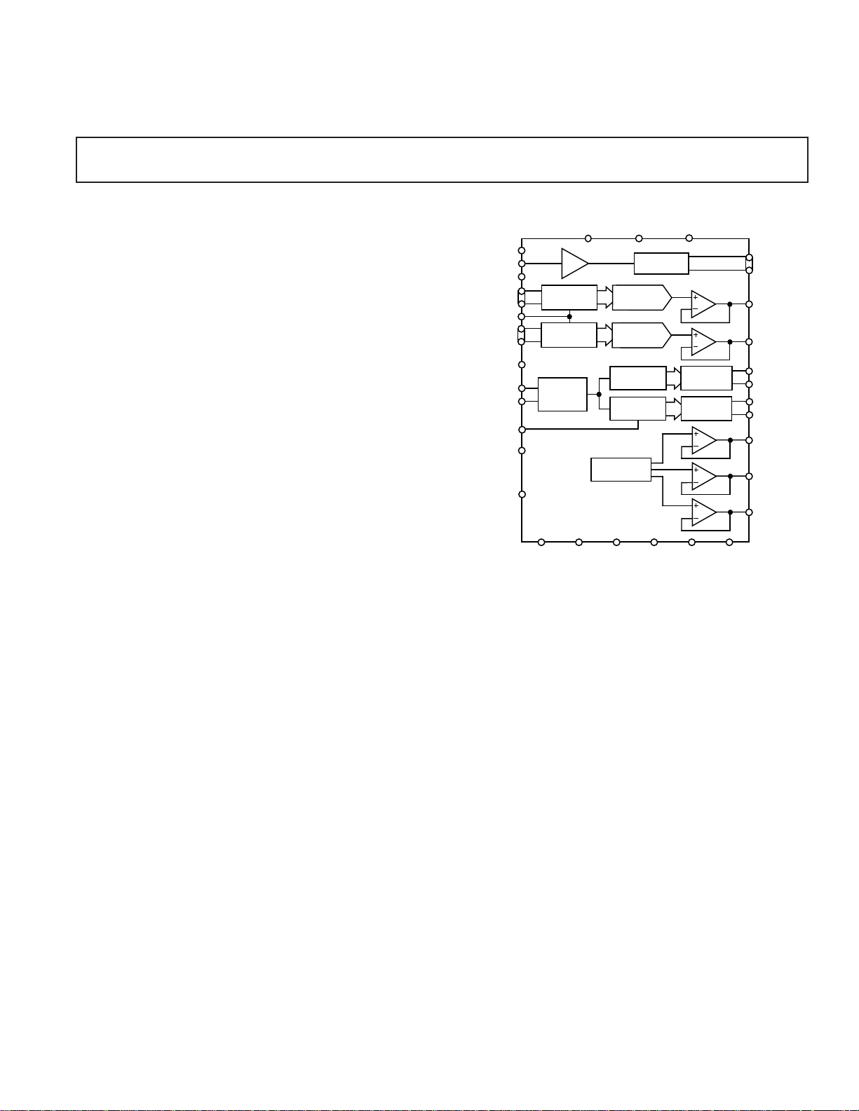
5 V Integrated High Speed ADC/Quad
DA7
DA0
VREFA
DVDD1
DGND1
AGND1
SDAC0F
DACA
AD7339
T/H
AVDD
DAC A
REGISTER
ADC
PARALLEL
DAC A
DB7
DB0
DACB
DACCLK
D0
D7
DAC 0
REGISTER
SERIAL
DAC 0
DAC 1
REGISTER
SERIAL
DAC 1
SERIAL
CONTROL
LOGIC
DAC B
REGISTER
PARALLEL
DAC B
2.5V
REFERENCE
SDAC0S
SDAC1F
SDAC1S
VREF
VREFB
ADCPDB
AIN
ADCCLK
DACPDB
SDATA
SCLK
LATCH
SDACPDB
DVDD2 DVDD3
DGND2
DGND3 AGND2 AGND3
a
FEATURES
8-Bit A/D Converter
Two 8-Bit D/A Converters
Two 8-Bit Serial D/A Converters
Single +5 V Supply Operation
On-Chip Reference
Power-Down Mode
52-Lead PQFP Package
GENERAL DESCRIPTION
The AD7339 is a composite IC that contains both DAC and
ADC functions. The device includes an 8-bit parallel A-to-D
converter. Two 8-bit parallel DACs are also included as are two
serial control DACs. These serial DACs are 8-bit DACs.
The AD7339, which operates with a single 5 V power supply,
has a bandgap reference on board with a nominal value of 2.5 V.
To reduce the power consumption of the part, each section,
except the reference, can be individually powered down when
not in use.
The AD7339 is available in a 52-lead PQFP package.
DAC System
AD7339
FUNCTIONAL BLOCK DIAGRAM
REV. 0
Information furnished by Analog Devices is believed to be accurate and
reliable. However, no responsibility is assumed by Analog Devices for its
use, nor for any infringements of patents or other rights of third parties
which may result from its use. No license is granted by implication or
otherwise under any patent or patent rights of Analog Devices.
One Technology Way, P.O. Box 9106, Norwood, MA 02062-9106, U.S.A.
Tel: 781/329-4700 World Wide Web Site: http://www.analog.com
Fax: 781/326-8703 © Analog Devices, Inc., 1997
Page 2
(AVDD = DVDD = +5 V 6 10%, AGND = DGND = 0 V, TA = T
± V
1
wise noted)
coupling with a 1 nF capacitor is needed if the bias
voltage does not equal 1.4 V. The input should be
driven with a maximum source impedance of 50 Ω.
11
SWING
DACB and VREFB
AD7339–SPECIFICATIONS
Parameter B Version Units Test Conditions/Comments
ADC ADCCLK = 2.048 MHz
Resolution 8 Bits
Differential Nonlinearity ±1 LSB max 8 Bits Monotonic
Integral Nonlinearity ±1 LSB max
Zero Input Offset Error ±3 LSB
Signal Range ±1 V max The input must be biased about 1.4 V. Therefore, ac
Full Power Input Bandwidth 1.024 MHz
Conversion Rate 2.048 MSPS
Signal to (Noise + Distortion) 42.7 dB min
Effective No. of Bits (ENOB) 6.8 Bits min
Intermodulation Distortion 48 dB min See Terminology
Error Rate 4.7 × 10
Input Capacitance 5 pF max
Coding Offset Binary 00H to FFH with 80H = 0 V
PARALLEL DACS DACCLK = 2.304 MHz
Resolution 8 Bits
Differential Nonlinearity ±1 LSB max 8 Bits Monotonic
Integral Nonlinearity ±1 LSB max
Output Signal Range V
V
SWING
V
BIAS
Update Rate 2.304 MHz max
Bipolar Zero Offset Error ±40 mV max Factory Trim. Does Not Include Gain Error
Gain Error ±5 % typ
Output Harmonic Content in 50 dB min For a Full-Scale Digital Sine Wave in Band 0 kHz to 76.8 kHz
Band 0 MHz to 1.152 MHz 46 dB min For a Full-Scale Digital Sine Wave in Band 0 kHz to 128 kHz
Gain Matching Between DACs 0.2 dB For Amplitudes Which Equal Full Scale –10 dB
Crosstalk 1.8 kΩ Load Between DACA and VREFA, and Between
To B Channel from A Channel 55 dB min A Channel has a full-scale output of frequency 128 kHz.
To A Channel from B Channel 55 dB min B Channel has a full-scale output of frequency 128 kHz.
To VREFB from A Channel 55 dB min A Channel has a full-scale output of frequency 128 kHz.
To VREFA from B Channel 55 dB min B Channel has a full-scale output of frequency 128 kHz.
Load Resistance 1.8 kΩ min Connected Between DACA/B and VREFA/B
Load Capacitance 50 pF max
Full-Scale Settling Time 4 µs typ
Coding Offset Binary 00H to FFH with 80H = Bias Voltage
BIAS
14/25 × VREFA/B V nom VREFA/B means VREFA for DACA and VREFB for DACB.
VREFA/B V nom
MIN
to T
MAX
, unless other-
SERIAL DACS SCLK is a gated 256 kHz clock.
Resolution 8 Bits
Differential Nonlinearity ±1 LSB 8 Bits Monotonic
Integral Nonlinearity ±1.5 LSB With Respect to Full Scale
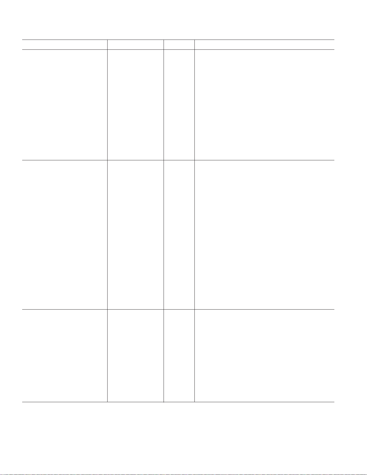
Output Range See Figure 1
00H 0.2 V max
FFH AVDD – 0.247 V min When AVDD > 5.247 V, the analog output will equal 2 VREF.
Update Rate SCLK/10 kHz max
Load Resistance 20 kΩ max
Load Capacitance 100 pF max
I
SINK
I
SOURCE
Full-Scale Settling Time 2.5 µs typ
Coding Straight Binary
1 mA typ
100 µA typ
–2–
REV. 0
Page 3
AD7339
Parameter B Version Units Test Conditions/Comments
REFERENCE
VREF Voltage 2.5 ± 2% V min/max
VREFA/VREFB Voltage 2.5 ± 5% V min/max
Load Capacitance 0.1 µF max Each reference output must have a load capacitance
of 100 pF minimum for compensation purposes.
I
SINK
I
SOURCE
LOGIC INPUTS
V
, Input High Voltage DVDD – 0.8 V min
INH
V
, Input Low Voltage 0.8 V max
INL
I
, Input Leakage Current 10 µA max
INH
CIN, Input Capacitance 15 pF max
LOGIC OUTPUTS
V
, Output High Voltage DVDD – 0.4 V min |I
OH
V
, Output Low Voltage 0.4 V max |I
OL
C
, Output Capacitance 15 pF max
OUT
POWER SUPPLIES
AVDD, DVDD 4.5/5.5 V min/max
I
DD
Power-Down Current 4.5 mA max +25°C. No Load on VREF
NOTES
1
Operating temperature range is as follows: B Version; –40° C to +85°C.
Specifications subject to change without notice.
1 mA max
1 mA max
| ≤ 1 mA
OUT
| ≤ 2 mA
OUT
45 mA max Active Mode
5 mA max –40°C to +85°C. No Load on VREF
2VREF
4.753
4.253
POWER
OUTPUT VOLTAGE – Volts
0.2
0 255
ANALOG OUTPUT VOLTAGE
SUPPLY
217 243
+4.5V
+5.5V
POWER
SUPPLY
+5V
POWER
SUPPLY
Figure 1. Analog Output Voltage from Serial DACs vs. Power Supply
REV. 0
–3–
Page 4
AD7339
TIMING CHARACTERISTICS
(AVDD = +5 V 6 10%; AGND = DGND = 0 V; TA = T
Limit at
Parameter TA = –408C to +858C Units Description
ADC See Figure 3.
t
1
t
2
t
3
t
4
t
5
480 ns min ADCCLK Period
210 ns min ADCCLK Width Low
210 ns min ADCCLK Width High
100 ns min Data Valid After Falling Edge of ADCCLK
200 ns min Data Valid Before Subsequent Falling Edge of ADCCLK
PARALLEL DACS See Figure 4.
t
6
t
7
t
8
t
9
t
10
t
11
t
12
430 ns min DACCLK Period
200 ns min DACCLK Width Low
200 ns min DACCLK Width High
130 ns min Data Setup Before DACCLK Rising Edge Time
50 ns min Data Hold After DACCLK Rising Edge Time
150 ns max Propagation Delay
250 ns max Settling Time (from 10% to 90%)
SERIAL DACS See Figure 5.
t
13
t
14
t
15
t
16
t
17
t
18
t
19
3.9 µs min SCLK Period
1.94 µs min SCLK Width Low
1.94 µs min SCLK Width High
950 ns min Data Setup Before SCLK Rising Edge
950 ns min Latch Enable Setup Time After SCLK Falling Edge
480 ns min LATCH Pulsewidth
100 µs max Conversion Delay
MlN
to T
, unless otherwise noted)
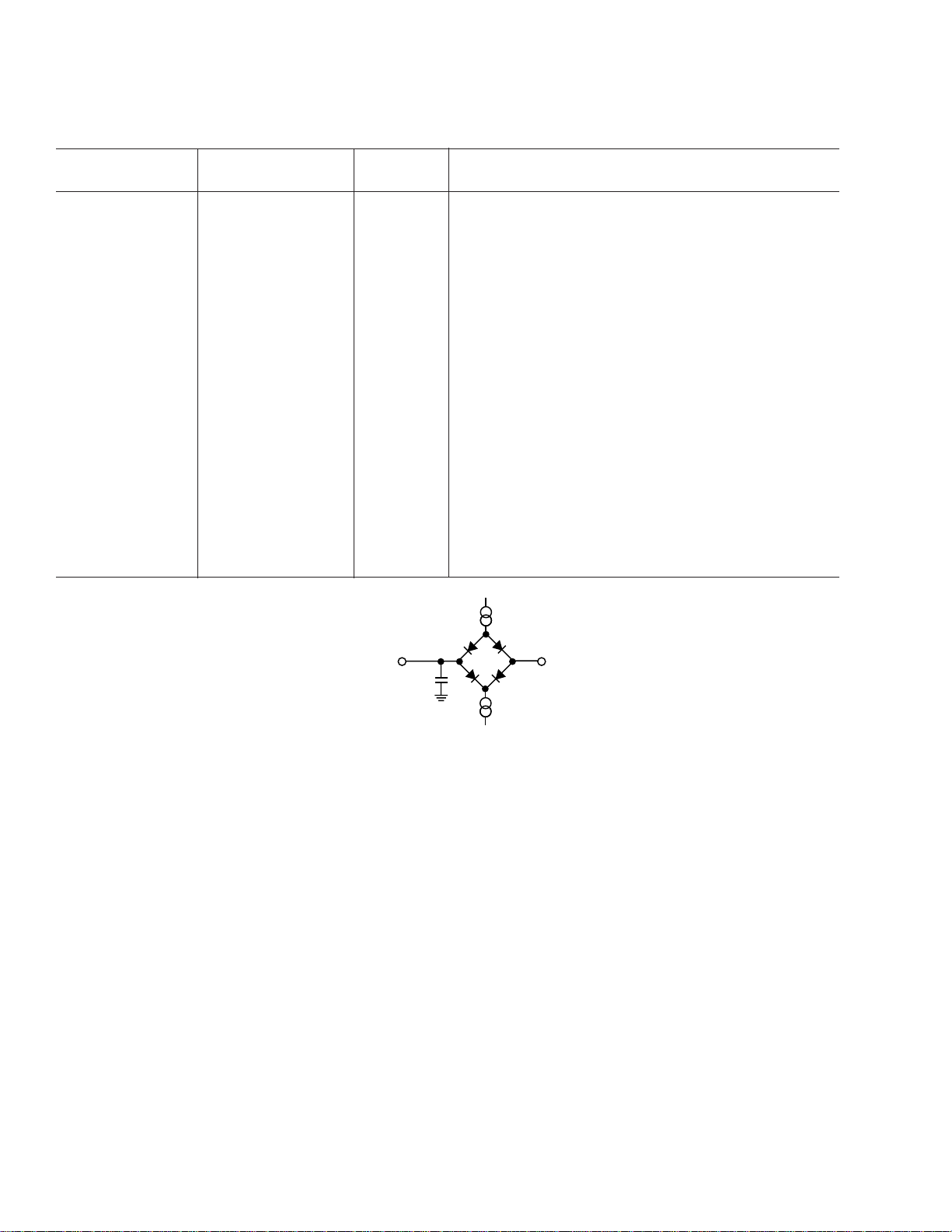
MAX
I
2mA
OL
TO
OUTPUT
PIN
15pF
C
L
I
1mA
OH
+2.1V
Figure 2. Load Circuit for Timing Specifications
–4–
REV. 0
Page 5

ADCCLK
AD7339
SAMPLE NSAMPLE N–1SAMPLE N–2 SAMPLE N+1 SAMPLE N+2
t
2
t
3
t
1
t
4
t
5
D0 – D7
SCLK
DACCLK
DA0 – DA7
DB0 – DB7
DACA
DACB
t
N–2
N+1NN–1N–3
Figure 3. ADC Timing
t
6
t
7
t
8
DATA
t
9
DATA
t
11
10%
t
12
90%
t
10
Figure 4. Parallel DACs Timing
14
t
15
t
13
t
16
REV. 0
SDATA
LATCH
SDAC0S
SDAC1S
D1
D0 D9(MSB) D8 D7
t
17
t
18
t
19
10%
Figure 5. Serial DACs Timing
–5–
Page 6

AD7339
ABSOLUTE MAXIMUM RATINGS
(T
= +25°C unless otherwise noted)
A
1
AVDD, DVDD to GND . . . . . . . . . . . . . . . . . –0.3 V to +7 V
AGND to DGND . . . . . . . . . . . . . . . . . . . . . –0.3 V to +0.3 V
Digital I/O Voltage to DGND . . . . . . –0.3 V to VDD + 0.3 V
ADC Analog Input Voltage . . . . . . . . . . . . . . . . . . . . . . . ±2 V
Input/Output Current at any Pin Except Supplies
2
. . . 20 mA
Operating Temperature Range
Industrial (B Version) . . . . . . . . . . . . . . . . . –40°C to +85°C
Storage Temperature Range . . . . . . . . . . . . –65°C to +150°C
Maximum Junction Temperature . . . . . . . . . . . . . . . .+150°C
PQFP, θ
Thermal Impedance . . . . . . . . . . . . . . . . . 90°C/W
JA
Lead Temperature, Soldering
Vapor Phase (60 sec) . . . . . . . . . . . . . . . . . . . . . . . . +215°C
Infrared (15 sec) . . . . . . . . . . . . . . . . . . . . . . . . . . . .+220°C
ORDERING GUIDE
Temperature Package Package
Model Range Description Option
AD7339BS –40°C to +85°C Plastic Quad Flatpack (PQFP) S-52
NOTES
1
Stresses above those listed under Absolute Maximum Ratings may cause permanent damage to the device. This is a stress rating only; functional operation of the
device at these or any other conditions above those listed in the operational sections
of this specification is not implied. Exposure to absolute maximum rating conditions for extended periods may affect device reliability.
2
Transient currents of up to 100 mA will not cause SCR latchup.
CAUTION
ESD (electrostatic discharge) sensitive device. Electrostatic charges as high as 4000 V readily
accumulate on the human body and test equipment and can discharge without detection.
Although this device features proprietary ESD protection circuitry, permanent damage may
occur on devices subjected to high energy electrostatic discharges. Therefore, proper ESD
precautions are recommended to avoid performance degradation or loss of functionality.
WARNING!
ESD SENSITIVE DEVICE
–6–
REV. 0
Page 7

PIN CONFIGURATION
DA7
52 51 50 49 48 43 42 41 4047 46 45 44
1
DACCLK
2
DVDD1
3
DB0
4
DB1
5
DB2
6
DB3
7
DB4
8
DB5
9
DB6
10
DB7
11
DACPDB
12
DGND1
SDACPDB
13
14 15 16 17 18 19 20 21 22 23 24 25 26
SCLK
PIN FUNCTION DESCRIPTIONS
Pin Number Mnemonic Function
DA5
DA6
PIN 1
IDENTIFIER
LATCH
SDATA
DA2
DA3
DA4
AD7339
TOP VIEW
(Not to Scale)
D5
D6
D7
DA1
D4
DA0
VREFA
DVDD2
DGND2
VREFB
DACA
D2
D3
DACB
D1
SDAC1S
39
38
37
36
35
34
33
32
31
30
29
28
27
D0
SDAC1F
SDAC0S
SDAC0F
AGND1
VREF
AGND3
AVDD
AGND
AIN
ADCPDB
DVDD3
DGND3
ADCCLK
AD7339
2
Power Supply
33 AVDD Analog power supply connection.
2 DVDD1 Digital power supply for the parallel DACs.
12 DGND1 Digital ground connection for the parallel DACs.
36 AGND1 Analog ground connection for the parallel DACs.
22 DVDD2 Digital power supply for the ADC.
29 DVDD3 Digital power supply for the ADC.
21 DGND2 Digital ground connection for the ADC.
28 DGND3 Digital ground connection for the ADC.
32 AGND2 Analog ground connection for the ADC.
34 AGND3 Analog ground connection for the reference.
ADCs
31 AIN Analog input to the ADC. The analog input must be appropriately ac coupled.
The AD7339 can accept an analog input of ± 1 V maximum.
27 ADCCLK ADC Input Clock, CMOS Logic Input. The analog input is sampled on the rising edge
of ADCCLK. ADCCLK is nominally set to 2.048 MHz.
26–23, 20–17 D0–D7 Digital Output from the ADC. The 8-bit digital word from the ADC is in offset binary.
The digital output uses CMOS logic.
30 ADCPDB Digital Input. When ADCPDB is low, the ADC is powered down. While in this mode,
ADCCLK should be tied low. The ADC is powered up by taking ADCPDB high.
Parallel DACs
45–52 DA0–DA7 Digital input to the parallel A DAC. The digital input uses CMOS logic and the word
is presented to the DAC in offset binary format.
3–10 DB0–DB7 Digital input to the parallel B DAC. The digital input uses CMOS logic and the word
is presented to the DAC in offset binary format.
1 DACCLK Input clock to the parallel DACs. The digital words in the A and B DAC registers are
loaded into the DACs on the rising edge of DACCLK. DACCLK has a nominal frequency of 2.304 MHz and uses CMOS logic.
43, 41 DACA, DACB Analog outputs from the A and B DACs. Both DACs have an analog output of VREFA/
VREFB ± X volts where VREFA = VREFB = 2.5 V nominal and X = 1.4 V.
REV. 0
–7–
Page 8

AD7339
Pin Number Mnemonic Function
11 DACPDB Digital Input. The parallel DACs, VREFA and VREFB, can be powered down
using pin DACPDB. When DACPDB is low, both of the parallel DACs and the
VREFA/VREFB outputs are placed in a standby mode, drawing a minimal current. The reference, which is available on the VREF pin, is not powered down.
Serial DACs
16 SDATA Serial Input Data. Serial data is latched into the AD7339 registers on the rising
edge of SCLK. The digital data uses CMOS logic. Data is loaded into the latches
in 10-bit bursts (MSB first), the 2 MSBs of the word indicating the DAC to which
the digital word is being loaded while the 8 LSBs contain the digital word being
loaded into the DAC. The serial DACs use offset binary.
14 SCLK Serial Input Clock. Data is latched into the registers on the rising edge of SCLK,
which is nominally set to 256 kHz. SCLK is a gated clock—the clock should be active
only when data is being loaded into the latches. The clock should idle low between
conversions.
15 LATCH Latch Enable Input. LATCH is used to load the digital data from the latch into
the DAC and begin conversion. Both DACs are loaded with the digital data in
their respective latches. LATCH is pulsed high to load the DACs, the DACs being
loaded on the rising edge of LATCH.
38 SDAC0S Analog Output from Serial DAC0. The analog output from this DAC will have a
value of 0.2 V to AVDD – 0.247 V.
37 SDAC0F Feedback Analog Input. By connecting a resistor between SDAC0F and SDAC0S,
the gain of the DAC0 buffer can be altered and the magnitude of the analog output adjusted accordingly.
40 SDAC1S Analog Output from Serial DAC1. The analog output from this DAC will have a
value of 0.2 V to AVDD – 0.247 V.
39 SDAC1F Feedback Analog Input. By connecting a resistor between SDAC1F and SDAC1S,
the gain of the DAC1 buffer can be altered and the magnitude of the analog output adjusted accordingly.
13 SDACPDB Digital Input. The serial DACs are powered down using SDACPDB. When this
pin is tied low, the serial DACs are placed in standby mode.
Reference
35 VREF The onboard bandgap reference is available on the VREF pin. The reference has a
value of 2.5 V nominal. A bypass capacitor of 0.1 µF is required between VREF
and AGND. This output cannot be powered down.
44, 42 VREFA/VREFB A buffered version of the reference is available on VREFA/VREFB. The analog
outputs from the parallel DACs are biased about the reference voltage. DACA is
biased about VREFA while DACB is biased about VREFB. VREFA and VREFB
can be used with DACA and DACB to provide differential analog inputs to the
circuitry connected to the DACs. These outputs are powered down using DACPDB.
These outputs should be decoupled using a capacitance of 100 pF minimum.
–8–
REV. 0
Page 9

AD7339
DA7
DA0
VREFB
DACA
AD7339
DAC A
REGISTER
DB7
DB0
DACB
DACCLK
CONTROL
LOGIC
DAC B
REGISTER
REFERENCE
VREFA
DACPDB
DAC A
DAC B
FUNCTIONAL DESCRIPTION
A-to-D Converter
The A/D conversion circuitry consists of a track-and-hold amplifier followed by a flash A-to-D converter. Figure 6 shows the
architecture of the ADC.
AD7339
D7
AIN
T/H
HOLD
REFERENCE
COMPARATOR
NETWORK
DECODE
LOGIC
OUTPUT
REGISTER
RESISTOR
LADDER
OUTPUT
DRIVERS
TIMING AND
CONTROL
LOGIC
ADCCLK ADCPDB
D6
D5
D4
D3
D2
D1
D0
Figure 6. ADC Architecture
Track-and-Hold Amplifier
The track-and-hold amplifier on the analog input of the AD7339’s
ADC allows the ADC to accurately convert input frequencies to
8-bit accuracy. The input bandwidth of the track-and-hold amplifier is much greater than the Nyquist rate of the ADC.
The operation of the track-and-hold is essentially transparent to
the user. The track-and-hold amplifier goes from its tracking
mode to its hold mode on the rising edge of ADCCLK.
Analog Input
The ADC accepts an analog input of 2 V p-p. The analog input
is biased about 1.4 V internally. If the signal applied to the ADC is
biased about 1.4 V, then dc coupling can be used. AC coupling
is needed if the analog input is biased about any voltage other
than 1.4 V. A capacitor of 1 nF is suitable for ac coupling.
Figure 7 shows the ideal input/output transfer function for the
ADC. The designed code transitions occur midway between
successive integer LSB values (1/2 LSB, 3/2 LSB, 5/2 LSB . . .)
with 1 LSB = FS/256 = 2 V/256 = 7.8 mV.
ADC OUTPUT
CODE
11111111
11111110
10000010
10000001
10000000
01111111
01111110
00000001
00000000
–1V
AD7339
ADC
0V
ANALOG INPUT VOLTAGE – AIN
+1V – 1LSB
Parallel DACs
The circuitry for each parallel DAC consists of a current source
DAC followed by a buffer that converts the current to a voltage.
Figure 8 shows the functional block diagram for the parallel
DACs.
The loading of both the A and B DAC is controlled by the
DACCLK signal, which is nominally set to 2.304 MHz. The
digital input to each DAC is latched in on the rising edge of the
DACCLK signal so that both DACs simultaneously perform the
D-to-A conversion.
Figure 8. Parallel DACs Functional Block Diagram
The analog output from each DAC is biased about the reference
voltage VREFA (DAC A) or VREFB (DAC B). The analog
output is ±1.4 V about the reference voltage. Since the analog
outputs are biased about the reference voltage, the reference
outputs can be used with the analog outputs to form a differential signal for the circuitry that follows the DACs.
The AD7339 includes a calibration feature that reduces the
offset between the DAC output bias voltage and the VREFA/
VREFB voltage. A 4-bit offset nulling feature is used to factory
trim the offset. The device also has a 4-bit offset register that is
user controlled; i.e., the user can disable the factory trimmed
offset and use the 4-bit register instead. This allows the user to
calibrate out the system offset; however, the user is also responsible for calibrating out the AD7339 offset.
The 4-bit offset register is accessed via the serial interface that is
used by DAC 0 and DAC 1. Table III gives the addresses for
accessing these registers. D5 of the 10-bit data word enables the
user to write to the 4-bit offset register. When this bit is set to 0,
the factory trimmed value is used as the offset value, while the
user programmed value is used when D5 equals 1. When the
offset is user controlled, D4 is used to inform the AD7339 to
reduce or increase the DAC output voltage. When D4 equals 0,
the DAC output is reduced, while the DAC output is increased
when D4 equals 1. When user trimming is being used, the 4-bit
word to be loaded into the register is contained in the 4 LSBs of
the 10-bit word being written to the serial port.
REV. 0
Figure 7. ADC Transfer Function
–9–
Page 10

AD7339
The 4-bit offset nulling feature has a LSB size of 7.6 mV; thereby,
allowing the user to vary the DAC output by ± 115 mV.
Table I. Writing to the Parallel DACs Offset Registers
D9 D8 D7 D6 D5 D4 D3 D2 D1 D0
Address X X Factory/ Decr/ Data Word
User Offset Incr
The DACs use offset binary coding with 1 LSB = FS/256 =
2.8/256 = 10.94 mV. Table II shows the ideal input code to
output voltage relationship.
Table II. Ideal Input/Output Code Table
DAC Latch Contents
MSB LSB Analog Output, V
OUT
*
00000000 –1.4 V
00000001 –1.38906 V
01111111 –0.01094 V
10000000 0 V
10000001 +0.01094 V
11111110 +1.37812 V
11111111 +1.38906 V
*These are the nominal output voltages with V
Serial DACs
= ±1.4 V.
OUT
The AD7339 has two serial DACs on board. The serial DACs
have an architecture similar to the parallel DACs. The 8-bit
digital word to each DAC is serially loaded. The serial DACs
have a common serial port. To distinguish between the two
DACs, 10-bit bursts are transferred to the DACs, the two MSBs
identifying the DAC to which the 8-bit word is to be loaded.
Table III shows the truth table for the two MSBs.
The serial word is loaded into the serial register using SDATA
and SCLK. SCLK is a gated clock of nominal value 256 kHz,
which should be active only when the 10-bit word is being
loaded into the register; i.e., SCLK should consist of 10 pulses.
If SCLK is continuous, or if it consists of more than 10 pulses,
the data shifted into the serial register will be shifted out of the
serial register so the register will not contain valid data. When
the serial register is not being written to, SCLK should idle low.
The serial data bits are read into the serial register on the rising
edge of SCLK, the two MSBs of the word identifying the DAC
to which the word is being written, and the eight LSBs of the
10-bit word containing the 8-bit word to be converted, the 8-bit
word being transferred MSB first. SDATA idles low.
Table III. Serial DACs Truth Table
D9 D8 DAC to be Written to
The 8-bit word is loaded into the DAC from the register using
LATCH. Data is loaded into the DACs on the falling edge of
LATCH. When the D-to-A conversion is performed, the analog
output is altered accordingly. The analog output will remain
valid until the next falling edge of LATCH, at which stage the
next digital word in the register is converted. LATCH is normally low, the input being pulsed to load the DACs, the DACs
being loaded on the falling edge of LATCH.
The analog output is available on the SDAC0S/SDAC1S pin.
Each DAC has an analog output of 0.2 V to AVDD – 0.247 V,
an input of 00H generating an analog output of 0.2 V while a
digital input of FFH produces an analog output of AVDD –
0.247 V, i.e., the serial DACs use straight binary coding. The
analog output is generated by the on board reference. Therefore, when AVDD is greater than 5.247 V, V
= 2 VREF
OUT
when the digital word equals all 1s. However, when AVDD is
less than 5.247 V, the output is limited to 0.247 V below AVDD
as the amplifier clips the output.
The output from the current source is converted to a voltage
using an operational amplifier. The amplifier is configured to
gain the signal by two; however, the gain of the amplifier can be
adjusted by tying a resistor between SDAC0F/SDAC1F and
SDAC0S/SDAC1S. The resistors on board the AD7339 have a
value of 20 kΩ.
Power-Down
Each section of the AD7339 can be individually powered down.
The ADC, parallel DACs and serial DACs have individual
power-down pins, which allows each section to be powered
down when it is not being used, thus minimizing the current
consumption of the AD7339.
Pin ADCPDB is used to place the ADC in sleep mode. When
this pin is taken low, the ADC is powered down. For normal
operation, ADCPDB is high.
When the parallel DACs are not being used, they can be placed
in power-down mode using DACPDB. When DACPDB is low,
both DACs are powered down. The reference outputs VREFA
and VREFB are also powered down. During power-down, the
analog outputs DACA and DACB, as well as the reference outputs, are pulled down to ground. When the DACs are powered up,
the analog outputs settle to the bias voltage VREFA/VREFB.
The serial DACs are powered down using SDACPDB. When
this pin is tied low, the serial DACs are placed in sleep mode.
When a converter is powered up, 100 µs are required for the
analog and digital circuitry to settle. Conversions can commence
when the circuitry has settled.
The reference on board the AD7339 is permanently powered
up. While the outputs VREFA and VREFB can be powered
down, the reference voltage, which is available on pin VREF, is
always available.
0 0 DAC A Offset Register Is Loaded
0 1 DAC 1 Register Is Loaded
1 0 DAC 0 Register Is Loaded
1 1 DAC B Offset Register Is Loaded
–10–
REV. 0
Page 11

AD7339
TERMINOLOGY
Differential Nonlinearity
The difference between the measured and the ideal 1 LSB change
between any two adjacent codes in the ADC or DACs. A speci-
fied Differential Nonlinearity of ±1 LSB max over the operating
temperature range ensures monotonicity.
Integral Nonlinearity
The maximum deviation of any code from a straight line passing
through the endpoints of the transfer function. The endpoints
of the transfer function are zero scale, a point 0.5 LSB below the
first code transition (000 . . . 00 to 000 . . . 01) and full scale, a
point 0.5 LSB above the last code transition (111 . . . 10 to
111 . . . 11). The error is expressed in LSBs.
Signal to (Noise + Distortion)
Signal to (Noise + Distortion) is measured signal-to-noise at the
output of the ADC. The signal is the rms magnitude of the
fundamental. Noise is the rms sum of all nonfundamental signals up to half the sampling frequency (F
/2) excluding dc.
S
Signal to (Noise + Distortion) is dependent on the number of
quantization levels used in the digitization process; the more
levels, the smaller the quantization noise. The theoretical signal
to (Noise + Distortion) ratio for a sine wave signal is given by
Signal to (Noise + Distortion) = (6.02N + 1.76) dB
where N is the number of bits. Thus for an ideal 8-bit converter,
Signal to (Noise + Distortion) is 49.92 dB.
ADC
Effective Number of Bits (ENOB)
Signal to (Noise + Distortion) is expressed in dBs; rewriting the
Signal to (Noise + Distortion) formula, it is possible to get a
measure of performance expressed in effective number of bits.
The effective number of bits for a device can be calculated directly from its measured Signal to (Noise + Distortion) value.
ENOB = (SNR – 1.76)/6.02
where SNR is the Signal to (Noise + Distortion).
Zero Input Offset Error
This is the offset error in the ADC when the analog input is
zero. Ideally, the digital output should equal 100 . . . 00. The
offset error is the deviation from the ideal output code. The
offset error is expressed in LSBs.
Intermodulation Distortion
With inputs consisting of sine waves at two frequencies, fa and
fb, any active device with nonlinearities will create distortion
products, of order (m + n), at sum and difference frequencies
of mfa ± nfb, where m, n = 0, 1, 2, 3, . . .. Intermodulation
terms are those for which m or n is not equal to zero. For the
AD7339, the Intermodulation Distortion is the level to which
the second and third intermodulation terms are suppressed
below a full scale output signal level, the second order terms
being (fa + fb) and (fa – fb) while the third order terms are
(2fa + fb), (2fa – fb), (fa + 2fb) and (fa – 2fb).
Error Rate
The rate at which A-to-D conversion errors occur.
DACS
Bipolar Zero Offset Error
The deviation between the measured output voltage and the
bias voltage (VREFA or VREFB, depending on which DAC is
being tested) when the DAC is loaded with code 100 . . . 00
after gain error has been adjusted out.
Gain Error
A measure of the output error between an ideal DAC and the
actual device output with all 1s loaded after offset error has been
adjusted out.
Update Rate
The rate at which the DACs can be loaded with new data. The
parallel DACs have an update rate of 2.304 MHz while the
serial DACs have an update rate of 256/10 kHz maximum.
Gain Matching Between DACs
The matching between the analog output amplitudes of the
parallel DACs when the same digital word is written to each
DAC.
Crosstalk
The ratio of the amplitude of a full-scale signal appearing on
one channel to the amplitude of the same signal which couples
onto another channel. Crosstalk is expressed in dBs.
Output Harmonic Content
When the digital word is converted to analog form, harmonics
will also be generated. The Output Harmonic Content specifies
the amount by which these harmonics are attenuated relative to
the fundamental frequency. With the parallel DACs, a full sine
wave of frequency 0 kHz to 128 kHz is input. The resulting
analog output is evaluated and the amount by which the
harmonics in the frequency band 0 MHz to 1.1152 MHz are
attenuated is measured relative to the magnitude of the fundamental output signal.
REV. 0
–11–
Page 12

AD7339
GROUNDING AND LAYOUT
The printed circuit board that houses the AD7339 should be
designed so that the analog and digital sections are separated
and confined to certain areas of the board. This facilitates the
use of ground planes that can be easily separated. A minimum
etch technique is generally best for ground planes as it gives the
best shielding.
Digital and analog ground planes should be joined in only one
place. If the AD7339 is the only device requiring an AGND-toDGND connection, the ground planes should be connected at
the AGND and DGND pins of the AD7339. If the AD7339 is
in a system where multiple devices require AGND-to-DGND
connections, the connection should be made at one point only,
a star point that should be established as close as possible to the
AD7339. Avoid running digital lines under the device as these
will couple noise onto the die. The analog ground plane should
be allowed to run under the AD7339 to avoid noise coupling.
The power supply lines to the AD7339 should use as large a
track as possible to provide low impedance paths and reduce the
effects of glitches on the power supply line. Fast switching signals such as clocks should be shielded with digital ground to
avoid radiating noise to other sections of the board. Avoid
crossover of digital and analog signals. Traces at opposite sides
of the board should run at right angles to each other. This will
reduce the effects of feedthrough through the board. A microstrip
technique is by far the best, but is not always possible with a
double-sided board. In this technique, the component side of
the board is dedicated to ground planes while signals are placed
on the other side. Good decoupling is important. The analog
and digital supplies to the AD7339 are independent and separately pinned out to minimize coupling between analog and
digital sections of the device. All analog and digital supplies
should be decoupled to AGND and DGND respectively using
0.1 µF ceramic capacitors in parallel with 10 µF tantalum
capacitors. To achieve the best from the decoupling capacitors, they should be placed as close as possible to the device,
ideally right up against the device. In systems where a common supply is used to drive both the AVDD and DVDD of
the AD7339, it is recommended that the system’s AVDD supply be used. This supply should have the recommended analog
supply decoupling between the AVDD pins of the AD7339 and
AGND and the recommended digital supply decoupling capacitors between the DVDD pins and DGND.
C3049–8–10/97
OUTLINE DIMENSIONS
Dimensions shown in inches and (mm).
52-Lead Plastic Quad Flatpack (PQFP)
(S-52)
52
1
13
14
0.557 (14.15)
0.537 (13.65)
0.398 (10.11)
0.390 (9.91)
PIN 1
TOP VIEW
(PINS DOWN)
0.0256
(0.65)
BSC
40
26
0.014 (0.35)
0.010 (0.25)
39
27
0.037 (0.95)
0.026 (0.65)
SEATING
PLANE
0.012 (0.30)
0.006 (0.15)
0.008 (0.20)
0.006 (0.15)
0.094 (2.39)
0.084 (2.13)
0.082 (2.09)
0.078 (1.97)
0.390 (9.91)
0.398 (10.11)
0.557 (14.15)
0.537 (13.65)
PRINTED IN U.S.A.
–12–
REV. 0
 Loading...