

Page 1
1 MSPS, 8-Channel, Software-Selectable,
–
True Bipolar Input, 12-Bit Plus Sign ADC
FEATURES
12-bit plus sign SAR ADC
True bipolar input ranges
Software-selectable input ranges
±10 V, ±5 V, ±2.5 V, 0 V to +10 V
1 MSPS throughput rate
Eight analog input channels with channel sequencer
Single-ended true differential and pseudo differential
analog input capability
High analog input impedance
and ADCIN pins allow separate access to mux and ADC
MUX
OUT
Low power: 21 mW
Temperature indicator
Full power signal bandwidth: 20 MHz
Internal 2.5 V reference
High speed serial interface
iCMOS™ process technology
24-lead TSSOP package
Power-down modes
GENERAL DESCRIPTION
The AD73291 is an 8-channel, 12-bit plus sign successive
approximation ADC designed on the iCMOS (industrial
CMOS) process. iCMOS is a process combining high voltage
CMOS and low voltage CMOS. It enables the development of
a wide range of high performance analog ICs capable of 33 V
operation in a footprint that no previous generation of high
voltage parts could achieve. Unlike analog ICs using conventional
CMOS processes, iCMOS components can accept bipolar input
signals while providing increased performance, dramatically
reduced power consumption, and reduced package size.
The AD7329 can accept true bipolar analog input signals. The
AD7329 has four software-selectable input ranges, ±10 V, ±5 V,
±2.5 V, and 0 V to +10 V. Each analog input channel can be
independently programmed to one of the four input ranges.
The analog input channels on the AD7329 can be programmed
to be single-ended, true differential, or pseudo differential.
The ADC contains a 2.5 V internal reference. The AD7329 also
allows for external reference operation. If a 3 V reference is
applied to the REF
IN
/REF
bipolar ±12 V analog input. The ADC has a high speed serial
interface that can operate at throughput rates up to 1 MSPS.
pin, the AD7329 can accept a true
OUT
AD7329
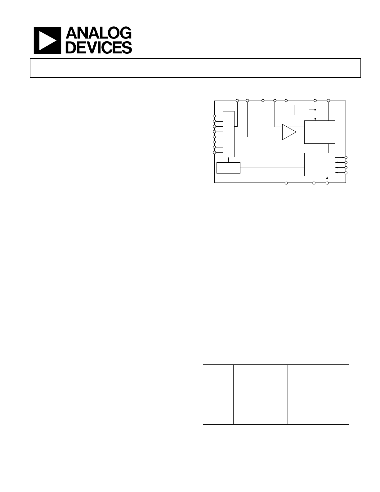
FUNCTIONAL BLOCK DIAGRAM
MUX
VIN0
V
V
V
V
V
V
V
+MUX
OUT
1
IN
2
IN
IN
IN
IN
IN
IN
3
4
5
6
7
I/P
MUX
CHANNEL
SEQUENCER
OUT
AD7329
ADCIN– ADCIN+
V
T/H
SS
Figure 1.
PRODUCT HIGHLIGHTS
1. The AD7329 can accept true bipolar analog input signals,
±10 V, ±5 V, ±2.5 V, and 0 V to +10 V unipolar signals.
2. The eight analog inputs can be configured as eight single-
ended inputs, four true differential input pairs, four pseudo
differential inputs, or seven pseudo differential inputs.
3. 1 MSPS serial interface. SPI®-/QSPI™-/DSP-/MICROWIRE™-
compatible interface.
4. Low power, 21 mW, at 1 MSPS.
5. MUX
the mux output prior to entering the ADC.
Table 1. Similar Devices
Device
Number Throughput Rate Number of Channels
AD7328 1000 kSPS 8
AD7327 500 kSPS 8
AD7324 1000 kSPS 4
AD7323 500 kSPS 4
AD7322 1000 kSPS 2
AD7321 500 kSPS 2
1
Protected by U.S. Patent No. 6,731,232.
and ADCIN pins allow for signal conditioning of
OUT
REFIN/REF
DD
2.5V
VREF
13-BIT SUCCESSIVE
OUT
APPROXIMAT ION
ADC
CONTROL
LOGIC AND
REGISTERS
AGNDV
V
CC
DOUT
SCLK
CS
DIN
V
DRIVE
05402-001
Rev. 0
Information furnished by Analog Devices is believed to be accurate and reliable. However, no
responsibility is assumed by Anal og Devices for its use, nor for any infringements of patents or ot her
rights of third parties that may result from its use. Specifications subject to change without notice. No
license is granted by implication or otherwise under any patent or patent rights of Analog Devices.
Trademarks and registered trademarks are the property of their respective owners.
One Technology Way, P.O. Box 9106, Norwood, MA 02062-9106, U.S.A.
Tel: 781.329.4700 www.analog.com
Fax: 781.461.3113 ©2006 Analog Devices, Inc. All rights reserved.
Page 2

AD7329
TABLE OF CONTENTS
Features.............................................................................................. 1
Registers........................................................................................... 25
Functional Block Diagram .............................................................. 1
General Description ......................................................................... 1
Product Highlights ........................................................................... 1
Revision History ............................................................................... 2
Specifications..................................................................................... 3
Timing Specifications .................................................................. 7
Absolute Maximum Ratings............................................................ 8
ESD Caution.................................................................................. 8
Pin Configuration and Function Descriptions............................. 9
Typical Performance Characteristics ........................................... 11
Terminology .................................................................................... 15
Theory of Operation ...................................................................... 17
Circuit Information.................................................................... 17
Converter Operation.................................................................. 17
Output Coding............................................................................ 18
Addressing Registers.................................................................. 25
Control Register ......................................................................... 26
Sequence Register....................................................................... 28
Range Registers........................................................................... 28
Sequencer Operation ..................................................................... 29
Reference ..................................................................................... 31
V
............................................................................................ 31
DRIVE
Temperature Indicator............................................................... 31
Modes of Operation ....................................................................... 32
Normal Mode.............................................................................. 32
Full Shutdown Mode.................................................................. 32
Autoshutdown Mode................................................................. 33
Autostandby Mode..................................................................... 33
Power vs. Throughput Rate....................................................... 34
Serial Interface ................................................................................ 35
Transfer Functions......................................................................18
Analog Input Structure.............................................................. 18
Track-and-Hold Section ............................................................ 19
Typical Connection Diagram ................................................... 20
Analog Input............................................................................... 20
Driver Amplifier Choice............................................................ 23
REVISION HISTORY
4/06—Revision 0: Initial Version
Microprocessor Interfacing........................................................... 36
AD7329 to ADSP-21xx.............................................................. 36
AD7329 to ADSP-BF53x........................................................... 36
Outline Dimensions....................................................................... 37
Ordering Guide .......................................................................... 37
Rev. 0 | Page 2 of 40
Page 3

AD7329
SPECIFICATIONS
VDD = 12 V to 16.5 V, VSS = −12 V to −16.5 V, VCC = 4.75 V to 5.25 V, V
= 1 MSPS, TA = T
MHz, f
S
directly to ADC
−, which is connected to GND for single-ended mode.
IN
MAX
to T
, unless otherwise noted. MUX
MIN
Table 2.
B Version
Parameter1 Min Typ Max Unit Test Conditions/Comments
DYNAMIC PERFORMANCE f
Signal-to-Noise Ratio (SNR)
2
76 77 dB Differential mode
72.5 74 dB Single-ended/pseudo differential mode
Signal-to-Noise + Distortion
(SINAD)
2
75 76.5 dB Differential mode; ±2.5 V and ±5 V ranges
76.5 dB Differential mode; 0 V to +10 V and ±10 V ranges
72 73.5 dB
73.5 dB
Total Harmonic Distortion (THD)2 −87 −80 dB Differential mode; ±2.5 V and ±5 V ranges
−85 dB Differential mode; 0 V to +10 V and ±10 V ranges
−82 −77 dB
−80 dB
Peak Harmonic or Spurious
Noise (SFDR)
2
−88 −80 dB Differential mode; ±2.5 V and ±5 V ranges
−86 dB Differential mode; 0 V to +10 V and ±10 V ranges
−84 −78 dB
−82 dB
Intermodulation Distortion
2
(IMD)
fa = 50 kHz, fb = 30 kHz
Second-Order Terms −88 dB
Third-Order Terms
Aperture Delay
Aperture Jitter
Common-Mode Rejection
(CMRR)
2
Channel-to-Channel Isolation
Full Power Bandwidth
3
3
−90 dB
7 ns
50 ps
−79 dB Up to 100 kHz ripple frequency; see
2
−75 dB
20 MHz At 3 dB
1.5 MHz At 0.1 dB
= 2.7 V to 5.25 V, V
DRIVE
+ is connected directly to ADCIN+ and MUX
OUT
= 50 kHz sine wave
IN
= 2.5 V internal/external, f
REF
Single-ended/pseudo differential mode; ±2.5 V and
±5 V ranges
Single-ended/pseudo differential mode; 0 V to +10 V
and ±10 V ranges
Single-ended/pseudo differential mode; ±2.5 V and
±5 V ranges
Single-ended/pseudo differential mode; 0 V to +10 V
and ±10 V ranges
Single-ended/pseudo differential mode; ±2.5 V and
±5 V ranges
Single-ended/pseudo differential mode; 0 V to +10 V
and ±10 V ranges
on unselected channels up to 100 kHz;
f
IN
Figure 14
see
SCLK
−is connected
OUT
Figure 17
= 20
Rev. 0 | Page 3 of 40
Page 4

AD7329
B Version
Parameter1 Min Typ Max Unit Test Conditions/Comments
DC ACCURACY4
Resolution 13 Bits
No Missing Codes
12-bit
Bits Differential mode
plus sign
11-bit
Bits Single-ended/pseudo differential mode
plus sign
Integral Nonlinearity
2
±1.1 LSB Differential mode
±1 LSB Single-ended/pseudo differential mode
−0.7/+1.2 LSB
Differential Nonlinearity2 −0.9/+1.5 LSB
±0.9 LSB
−0.7/+1 LSB
Offset Error
2, 5
−4/+9 LSB Single-ended/pseudo differential mode
−7/+10 LSB Differential mode
Offset Error Match
2, 5
±0.6 LSB Single-ended/pseudo differential mode
±0.5 LSB Differential mode
Gain Error
2, 5
±8.0 LSB Single-ended/pseudo differential mode
±14 LSB Differential mode
Gain Error Match
2, 5
±0.5 LSB Single-ended/pseudo differential mode
±0.5 LSB Differential mode
Positive Full-Scale Error
2, 6
±4 LSB Single-ended/pseudo differential mode
±7 LSB Differential mode
Positive Full-Scale Error Match
2, 6
±0.5 LSB Single-ended/pseudo differential mode
±0.5 LSB Differential mode
Bipolar Zero Error
2, 6
±8.5 LSB Single-ended/pseudo differential mode
±7.5 LSB Differential mode
Bipolar Zero Error Match
2, 6
±0.5 LSB Single-ended/pseudo differential mode
±0.5 LSB Differential mode
Negative Full-Scale Error
2, 6
±4 LSB Single-ended/pseudo differential mode
±6 LSB Differential mode
Negative Full-Scale Error Match
2, 6
±0.5 LSB Single-ended/pseudo differential mode
±0.5 LSB Differential mode
All dc accuracy specifications are typical for
0 V to 10 V mode.
Single-ended/pseudo differential mode
(LSB = FSR/8192)
Differential mode; guaranteed no missing codes to
13 bits
Single-ended mode; guaranteed no missing codes to
12 bits
Single-ended/psuedo differential mode
(LSB = FSR/8192)
Rev. 0 | Page 4 of 40
Page 5

AD7329
B Version
Parameter1 Min Typ Max Unit Test Conditions/Comments
ANALOG INPUT
Input Voltage Ranges Reference = 2.5 V; see Table 6
(Programmed via Range
±10 V V
Register)
±5 V VDD = 5 V min, VSS = −5 V min, VCC = 2.7 V to 5.25 V
±2.5 V VDD = 5 V min, VSS = − 5 V min, VCC = 2.7 V to 5.25 V
0 to 10 V VDD = 10 V min, VSS = AGND min, VCC = 2.7 V to 5.25 V
Pseudo Differential VIN−
Input Range
±3.5 V Reference = 2.5 V; range = ±10 V
±6 V Reference = 2.5 V; range = ±5 V
±5 V Reference = 2.5 V; range = ±2.5 V
+3/−5 V Reference = 2.5 V; range = 0 V to +10 V
DC Leakage Current ±100 nA VIN = VDD or VSS
3 nA Per channel, VIN = VDD or VSS
Input Capacitance3 16 pF When in track, all ranges, single ended
ADCIN± Capacitance3 7 pF When in track, ±10 V range, single ended
10 pF When in track, ±5 V range, single ended
14.5 pF When in track, ±2.5 V range, single ended
10.5 pF When in track, 0 V to +10 V range, single ended
4.0 pF When in hold, all ranges, single ended
MUX
− Capacitance3 7.5 pF All ranges, single ended
OUT
MUX
+ Capacitance3 13 pF All ranges, single ended
OUT
REFERENCE INPUT/OUTPUT
Input Voltage Range 2.5 3 V
Input DC Leakage Current ±1 μA
Input Capacitance 10 pF
Reference Output Voltage 2.5 V
Reference Output Voltage Error
±5 mV
@ 25°C
Reference Output Voltage
to T
MAX
T
MIN
Reference Temperature
±10 mV
25 ppm/°C
Coefficient
3 ppm/°C
Reference Output Impedance 7 Ω
LOGIC INPUTS
Input High Voltage, V
Input Low Voltage, V
2.4 V
INH
0.8 V VCC = 4.75 V to 5.25 V
INL
0.4 V VCC = 2.7 to 3.6 V
Input Current, IIN ±1 μA V
Input Capacitance, C
3
IN
10 pF
LOGIC OUTPUTS
Output High Voltage, VOH
V
DRIVE
V I
−
0.2 V
Output Low Voltage, VOL 0.4 V I
Floating-State Leakage Current ±1 μA
Floating-State Output
Capacitance
3
5 pF
Output Coding Straight natural binary Coding bit set to 1 in control register
Twos complement Coding bit set to 0 in control register
= 10 V min, VSS = −10 V min, VCC = 2.7 V to 5.25 V
DD
= 16.5 V, VSS = −16.5 V, VCC = 5 V; see Figure 43 and
V
DD
Figure 44
= 0 V or V
IN
= 200 μA
SOURCE
= 200 μA
SINK
DRIVE
Rev. 0 | Page 5 of 40
Page 6

AD7329
B Version
Parameter1 Min Typ Max Unit Test Conditions/Comments
CONVERSION RATE
Conversion Time 800 ns 16 SCLK cycles with SCLK = 20 MHz
Track-and-Hold Acquisition
2, 3
Time
300 ns Full-scale step input; see the
Throughput Rate 1 MSPS See the Serial Interface section; VCC = 4.75 V to 5.25 V
770 kSPS VCC < 4.75 V
POWER REQUIREMENTS Digital inputs = 0 V or V
VDD 12 16.5 V See Table 6
VSS −12 −16.5 V See Tab le 6
VCC 2.7 5.25 V See Table 6; typical specifications for VCC < 4.75 V
V
2.7 5.25 V
DRIVE
Normal Mode (Static) 0.9 mA VDD= 16.5, VSS = −16.5 V, VCC = V
Normal Mode (Operational) f
SAMPLE
= 1 MSPS
IDD 360 μA VDD = 16.5 V
ISS 410 μA VSS = −16.5 V
ICC and I
Autostandby Mode (Dynamic) f
3.2 mA VCC = V
DRIVE
SAMPLE
= 5.25 V
DRIVE
= 250 kSPS
IDD 200 μA VDD = 16.5 V
ISS 210 μA VSS = −16.5 V
ICC and I
1.3 mA VCC = V
DRIVE
DRIVE
= 5.25 V
Autoshutdown Mode (Static) SCLK on or off
IDD 1 μA VDD = 16.5 V
ISS 1 μA VSS = −16.5 V
ICC and I
1 μA VCC = V
DRIVE
DRIVE
= 5.25 V
Full Shutdown Mode SCLK on or off
IDD 1 μA VDD = 16.5 V
ISS 1 μA VSS = −16.5 V
ICC and I
1 μA VCC = V
DRIVE
DRIVE
= 5.25 V
POWER DISSIPATION
Normal Mode (Operational) 30 mW VDD = 16.5 V, VSS = −16.5 V, VCC = 5.25 V
21 mW VDD = 12 V, VSS = −12 V, VCC = 5 V
Full Shutdown Mode 38.25 μW VDD = 16.5 V, VSS = −16.5 V, VCC = 5.25 V
1
Temperature range is −40°C to +85°C.
2
See the Terminology section.
3
Sample tested during initial release to ensure compliance.
4
For dc accuracy specifications, the LSB size for differential mode is FSR/8192. For single-ended mode/pseudo differential mode, the LSB size is FSR/4096, unless
otherwise noted.
5
Unipolar 0 V to 10 V range with straight binary output coding.
6
Bipolar range with twos complement output coding.
Terminology section
DRIVE
= 5.25 V
DRIVE
Rev. 0 | Page 6 of 40
Page 7
AD7329
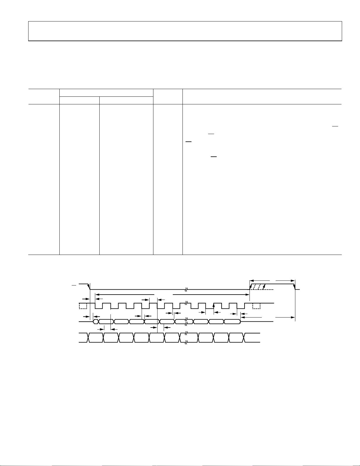
TIMING SPECIFICATIONS
VDD = 12 V to 16.5 V, VSS = −12 V to −16.5 V, VCC = 4.75 V to 5.25 V, V
. Timing specifications apply with a 32 pF load, unless otherwise noted. MUX
T
MIN
connected directly to ADC
−, which is connected to GND for single-ended mode.
IN
Table 3.
Limit at T
MIN
, T
MAX
Description
Parameter VCC < 4.75 V VCC = 4.75 V to 5.25 V Unit V
f
SCLK
50 50 kHz min
14 20 MHz max
t
CONVER T
t
75 60 ns min
QUIET
t
1
1
t
2
16 × t
16 × t
SCLK
ns max t
SCLK
12 5 ns min
25 20 ns min
45 35 ns min Unipolar input range (0 V to 10 V)
t
3
t
4
t5 0.4 × t
t6 0.4 × t
t
7
t
8
26 14 ns max
57 43 ns max Data access time after SCLK falling edge
SCLK
0.4 × t
SCLK
0.4 × t
SCLK
ns min SCLK high pulse width
SCLK
ns min SCLK low pulse width
13 8 ns min SCLK to data valid hold time
40 22 ns max SCLK falling edge to DOUT high impedance
10 9 ns min SCLK falling edge to DOUT high impedance
t
9
t
10
t
POWER-UP
1
When using VCC = 4.75 V to 5.25 V and the 0 V to 10 V unipolar range, running at 1 MSPS throughput rate with t2 at 20 ns, the mark space ratio needs to be limited to 50:50.
4 4 ns min DIN set-up time prior to SCLK falling edge
2 2 ns min DIN hold time after SCLK falling edge
750 750 ns max Power-up from autostandby
500 500 μs max
25 25 μs typ
CS
t
CONVERT
t
6
t
7
t
4
t
10
Figure 2. Serial Interface Timing Diagram
SCLK
DOUT
DIN
THREE-
STATE
t
2
12345 13141516
3 IDENTIFICATION BITS
t
3
ADD1
ADD2
WRITE
ADD0 SIGN DB11 DB10 DB2 DB1 DB0
t
9
REG
REG
SEL1
SEL2
= 2.7 V to 5.25 V, V
DRIVE
OUT
≤ VCC
DRIVE
SCLK
= 1/f
SCLK
+ is connected directly to ADCIN+ and MUX
= 2.5 V internal/external, TA = T
REF
MAX
OUT
to
−is
Minimum time between end of serial read and next falling edge of CS
Minimum CS
to SCLK set-up time; bipolar input ranges (±10 V, ±5 V, ±2.5 V)
CS
Delay from CS
pulse width
until DOUT three-state disabled
Power-up from full shutdown/autoshutdown mode, internal
reference
Power-up from full shutdown/autoshutdown mode, external
reference
t
1
t
5
LSB 0MSB
t
8
THREE-STATE
t
QUIET
05402-002
Rev. 0 | Page 7 of 40
Page 8
AD7329
ABSOLUTE MAXIMUM RATINGS
TA = 25°C, unless otherwise noted
Table 4.
Parameter Rating
VDD to AGND, DGND −0.3 V to +16.5 V
VSS to AGND, DGND +0.3 V to −16.5 V
VDD to VCC V
− 0.3 V to +16.5 V
CC
VCC to AGND, DGND −0.3 V to +7 V
V
to AGND, DGND −0.3 V to +7 V
DRIVE
AGND to DGND −0.3 V to +0.3 V
Analog Input Voltage to AGND1 V
− 0.3 V to VDD + 0.3 V
SS
Digital Input Voltage to DGND −0.3 V to +7 V
Digital Output Voltage to GND −0.3 V to V
DRIVE
+ 0.3 V
REFIN to AGND −0.3 V to VCC + 0.3 V
Input Current to Any Pin
Except Supplies
2
±10 mA
Operating Temperature Range −40°C to +85°C
Storage Temperature Range −65°C to +150°C
Junction Temperature 150°C
TSSOP Package
θJA Thermal Impedance 128°C/W
θJC Thermal Impedance 42°C/W
Pb-Free Temperature, Soldering
Reflow 260(0)°C
ESD 2.5 kV
1
If the analog inputs are being driven from alternative VDD and VSS supply
circuitry, Schottky diodes should be placed in series with the AD7329’s VDD
and VSS supplies.
2
Transient currents of up to 100 mA do not cause SCR latch-up.
Stresses above those listed under Absolute Maximum Ratings
may cause permanent damage to the device. This is a stress
rating only; functional operation of the device at these or any
other conditions above those indicated in the operational
section of this specification is not implied. Exposure to absolute
maximum rating conditions for extended periods may affect
device reliability.
ESD CAUTION
ESD (electrostatic discharge) sensitive device. Electrostatic charges as high as 4000 V readily accumulate on
the human body and test equipment and can discharge without detection. Although this product features
proprietary ESD protection circuitry, permanent damage may occur on devices subjected to high energy
electrostatic discharges. Therefore, proper ESD precautions are recommended to avoid performance
degradation or loss of functionality.
Rev. 0 | Page 8 of 40
Page 9
AD7329
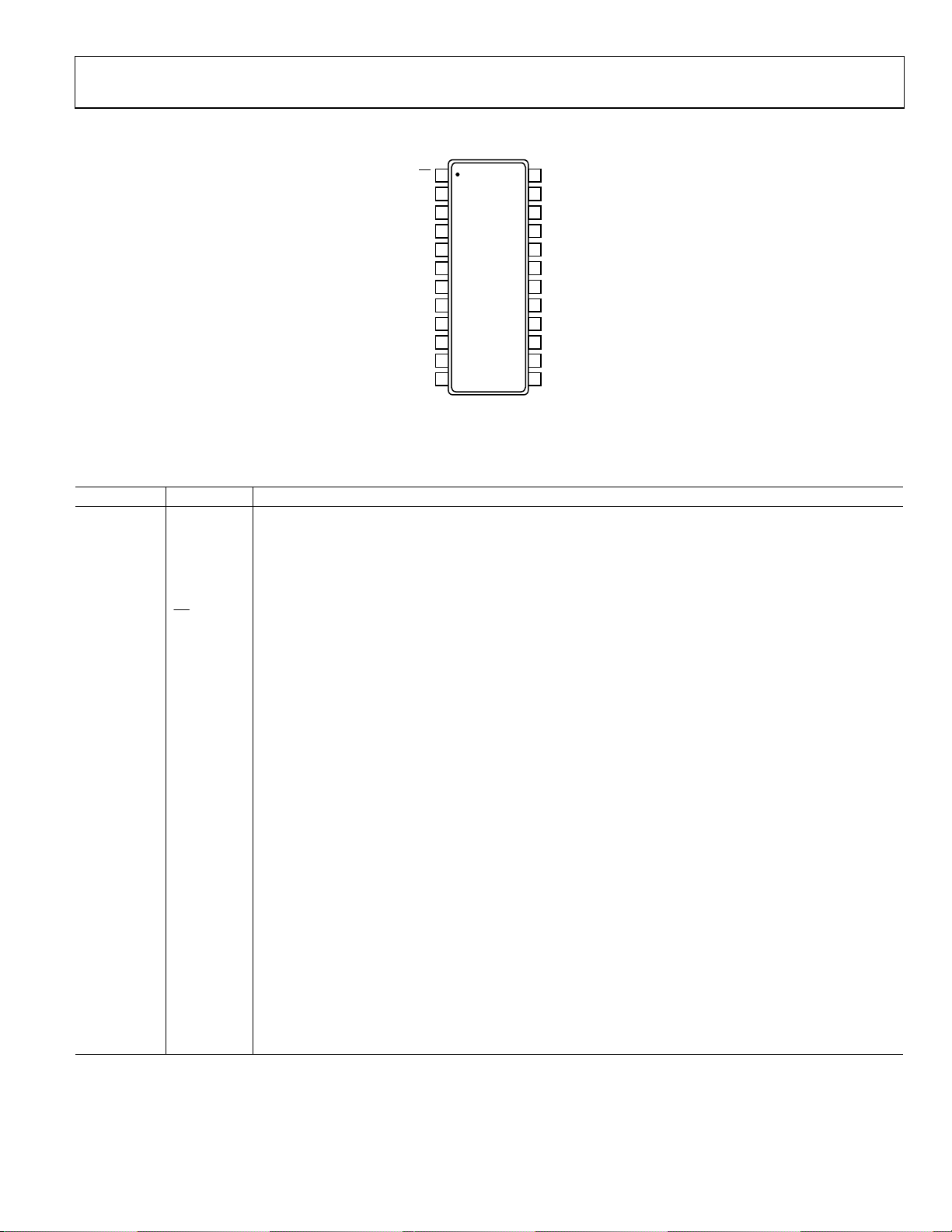
PIN CONFIGURATION AND FUNCTION DESCRIPTIONS
REFIN/REF
ADC
MUX
DIN
DGND
AGND
OUT
V
OUT
V
V
V
V
CS
SS
IN
IN
IN
IN
IN
+
+
0
10
1
4
11
12
5
1
2
3
4
AD7329
5
TOP VIEW
(Not to Scale)
6
7
8
9
24
23
22
21
20
19
18
17
16
15
14
13
SCLK
DGND
DOUT
V
DRIVE
V
CC
V
DD
ADCIN–
MUX
OUT
V
2
IN
3
V
IN
6
V
IN
7
V
IN
–
05402-003
Figure 3. TSSOP Pin Configuration
Table 5. Pin Function Descriptions
Pin No. Mnemonic Descriptions
24 SCLK
Serial Clock, Logic Input. A serial clock input provides the SCLK used for accessing the data from the AD7329.
This clock is also used as the clock source for the conversion process.
22 DOUT
Serial Data Output. The conversion output data is supplied to this pin as a serial data stream. The bits are
clocked out on the falling edge of the SCLK input, and 16 SCLKs are required to access the data. The data
stream consists of three channel identification bits, the sign bit, and 12 bits of conversion data. The data is
Serial Interface section).
1
provided MSB first (see the
Chip Select. Active low logic input. This input provides the dual function of initiating conversions on the
CS
AD7329 and frames the serial data transfer.
2 DIN
Data In. Data to be written to the on-chip registers is provided on this input and is clocked into the register
on the falling edge of SCLK (see the Registers section).
21 V
3, 23 DGND
DRIVE
Logic Power Supply Input. The voltage supplied at this pin determines at what voltage the interface operates.
This pin should be decoupled to DGND. The voltage at this pin can be different than that at V
not exceed V
by more than 0.3 V.
CC
but should
CC
Digital Ground. Ground reference point for all digital circuitry on the AD7329. The DGND and AGND voltages
ideally should be at the same potential and must not be more than 0.3 V apart, even on a transient basis.
4 AGND
Analog Ground. Ground reference point for all analog circuitry on the AD7329. All analog input signals and
any external reference signal should be referred to this AGND voltage. The AGND and DGND voltages ideally
should be at the same potential and must not be more than 0.3 V apart, even on a transient basis.
5 REFIN/REF
Reference Input/Reference Output. The on-chip reference is available on this pin for use external to the
OUT
AD7329. Alternatively, the internal reference can be disabled and an external reference applied to this input.
On power up, this is the default condition. The nominal internal reference voltage is 2.5 V, which appears at
Reference section).
20 VCC
this pin. A 680 nF capacitor should be placed on the reference pin (see the
Analog Supply Voltage, 2.7 V to 5.25 V. This is the supply voltage for the ADC core on the AD7329. This supply
should be decoupled to AGND.
19 VDD Positive Power Supply Voltage. This is the positive supply voltage for the analog input section.
6 VSS Negative Power Supply Voltage. This is the negative supply voltage for the analog input section.
7 ADCIN+
Positive ADC Input. This pin allows access to the on-chip track-and-hold. The voltage applied to this pin is still
a high voltage signal (±10 V, ±5 V, ±2.5 V, or 0 V to +10 V).
8 MUX
OUT
+
Positive Multiplexer Output. The output of the multiplexer appears at this pin. The voltage at this pin is still a
high voltage signal equivalent to the voltage applied to the V
+ input channel, as selected in the control
IN
register or sequence register. If no external filtering or buffering is required, this pin should be tied to the
ADCIN+ pin.
Rev. 0 | Page 9 of 40
Page 10

AD7329
Pin No. Mnemonic Descriptions
17 MUX
18 ADCIN−
9 to 16 VIN0 to VIN7
OUT
−
Negative Multiplexer Output. This pin allows access to the on-chip track-and-hold. The voltage applied to this
pin is still a high voltage signal when the AD7329 is in differential mode. When the AD7329 is in single-ended
mode, this signal is AGND, and MUX
pseudo differential mode, a small dc voltage appears at this pin, and this pin should be tied to the ADC
Negative ADC Input. This pin allows access to the track-and-hold. When the AD7329 is in single-ended mode,
this pin can be tied to MUX
mode, this pin should be connected to MUX
applied to this pin is a high voltage signal (±10 V, ±5 V, ±2.5 V, or 0 V to +10 V).
Analog Input 0 Through Analog Input 7. The analog inputs are multiplexed into the on-chip track-and-hold.
The analog input channel for conversion is selected by programming the channel address bits, ADD2
through ADD0, in the control register. The inputs can be configured as eight single-ended inputs, four true
differential input pairs, four pseudo differential inputs, or seven pseudo differential inputs. The configuration
of the analog inputs is selected by programming the mode bits, Mode 1 and Mode 0, in the control register.
The input range on each input channel is controlled by programming the range registers. Input ranges of
±10 V, ±5 V, ±2.5 V, or 0 V to +10 V can be selected on each analog input channel (see the
section). On power up, V
− can be connected directly to the ADCIN− pin. When the AD7329 is in
OUT
−, which is connected to AGND. When the AD7329 is in pseudo differential
OUT
−. When the AD7329 is in true differential mode, the voltage
OUT
Range Registers
0 is automatically selected and the voltage on this pin appears on MUX
IN
OUT
IN
+.
− pin.
Rev. 0 | Page 10 of 40
Page 11
AD7329
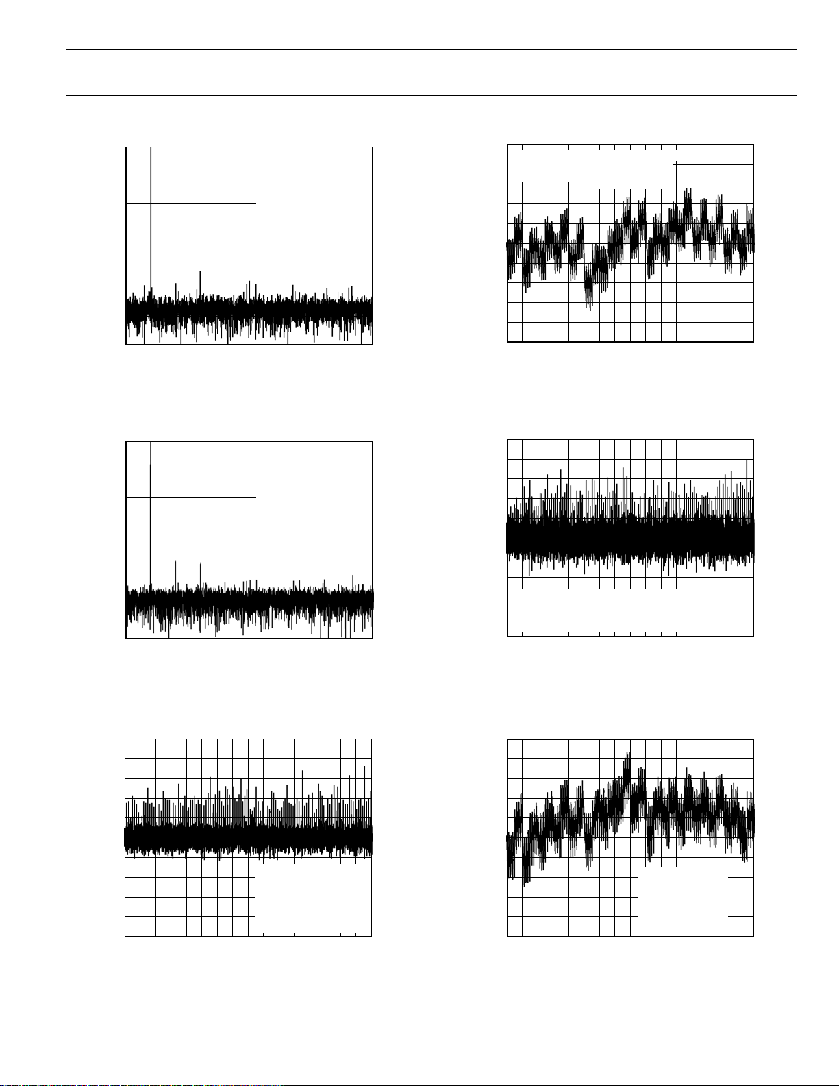
TYPICAL PERFORMANCE CHARACTERISTICS
1.0
VCC = V
0.8
T
= 25°C
A
V
DD
0.6
0.4
0.2
0
–0.2
INL ERROR (L SB)
–0.4
–0.6
–0.8
–1.0
0 8192
512 1536 2560 3584 4608 5632 6656 7680
= 5V
DRIVE
= 15V, VSS = –15V
1024 2048 3072 4096 5120 6144 7168
INT/EXT 2.5V REFERENCE
±10V RANGE
+INL = +0.55LSB
–INL = –0.68L SB
CODE
Figure 7. Typical INL True Differential Mode
05402-007
SNR (dB)
–20
–40
–60
–80
–100
–120
–140
0
0
50 100 150 200 250 300 350 400 450
FREQUENCY (kHz)
4096 POINT FFT
V
= V
CC
= 15V, VSS = –15V
V
DD
= 25°C
T
A
INT/EXT 2.5V REFERE NCE
±10V RANGE
f
= 50kHz
IN
SNR = 77.30dB
SINAD = 76.85dB
THD = –86.96dB
SFDR = –88.22d B
Figure 4. FFT True Differential Mode
DRIVE
= 5V
500
05402-004
SNR (dB)
–20
–40
–60
–80
–100
–120
–140
0
0
50 100 150 200 250 300 350 400 450
FREQUENCY (kHz)
4096 POINT FFT
= V
V
CC
V
DD
T
A
INT/EXT 2.5V REFERE NCE
±10V RANGE
f
IN
SNR = 74.67dB
SINAD = 74.03dB
THD = –82.68dB
SFDR = –85.40d B
= 5V
DRIVE
= 15V, VSS = –15V
= 25°C
= 50kHz
Figure 5. FFT Single-Ended Mode
1.0
0.8
0.6
0.4
0.2
0
–0.2
DNL ERROR (LSB)
–0.4
–0.6
–0.8
–1.0
0 8192
1024 2048 3072 4096 5120 6144 7168
512 1536 2560 3584 4608 5632 6656 7680
VCC = V
DRIVE
T
= 25°C
A
V
= 15V, VSS = –15V
DD
INT/EXT 2.5V REFERENCE
±10V RANGE
+DNL = +0.72LSB
–DNL = –0.22LSB
CODE
= 5V
Figure 6. Typical DNL True Differential Mode
500
1.0
0.8
0.6
0.4
0.2
0
–0.2
DNL ERROR (LSB)
–0.4
VCC = V
–0.6
T
= 25°C
A
V
–0.8
DD
INT/EXT 2.5V REFERE NCE
–1.0
0 8192
05402-005
512 1536 2560 3584 4608 5632 6656 7680
= 5V
DRIVE
= 15V, VSS = –15V
1024 2048 3072 4096 5120 6144 7168
±10V RANGE
+DNL = +0.79LSB
–DNL = –0.38L SB
CODE
05402-008
Figure 8. Typical DNL Single-Ended Mode
1.0
0.8
0.6
0.4
0.2
0
–0.2
INL ERROR (LSB)
–0.4
–0.6
–0.8
–1.0
0 8192
1024 2048 3072 4096 5120 6144 7168
05402-006
512 1536 2560 3584 4608 5632 6656 7680
VCC = V
DRIVE
T
= 25°C
A
V
= 15V, VSS = –15V
DD
INT/EXT 2.5V REFERENCE
±10V RANGE
+INL = +0.87LSB
–INL = –0.49L SB
CODE
= 5V
05402-009
Figure 9. Typical INL Single-Ended Mode
Rev. 0 | Page 11 of 40
Page 12
AD7329
–
–
–
50
VCC= V
V
DD
–55
T
A
f
= 1MSPS
S
–60
INTERNAL REFERENCE
AD8021 BETWEEN MUX
AND ADC
–65
–70
0V TO +10V RANG E
–75
THD (dB)
–80
–85
–90
–95
10
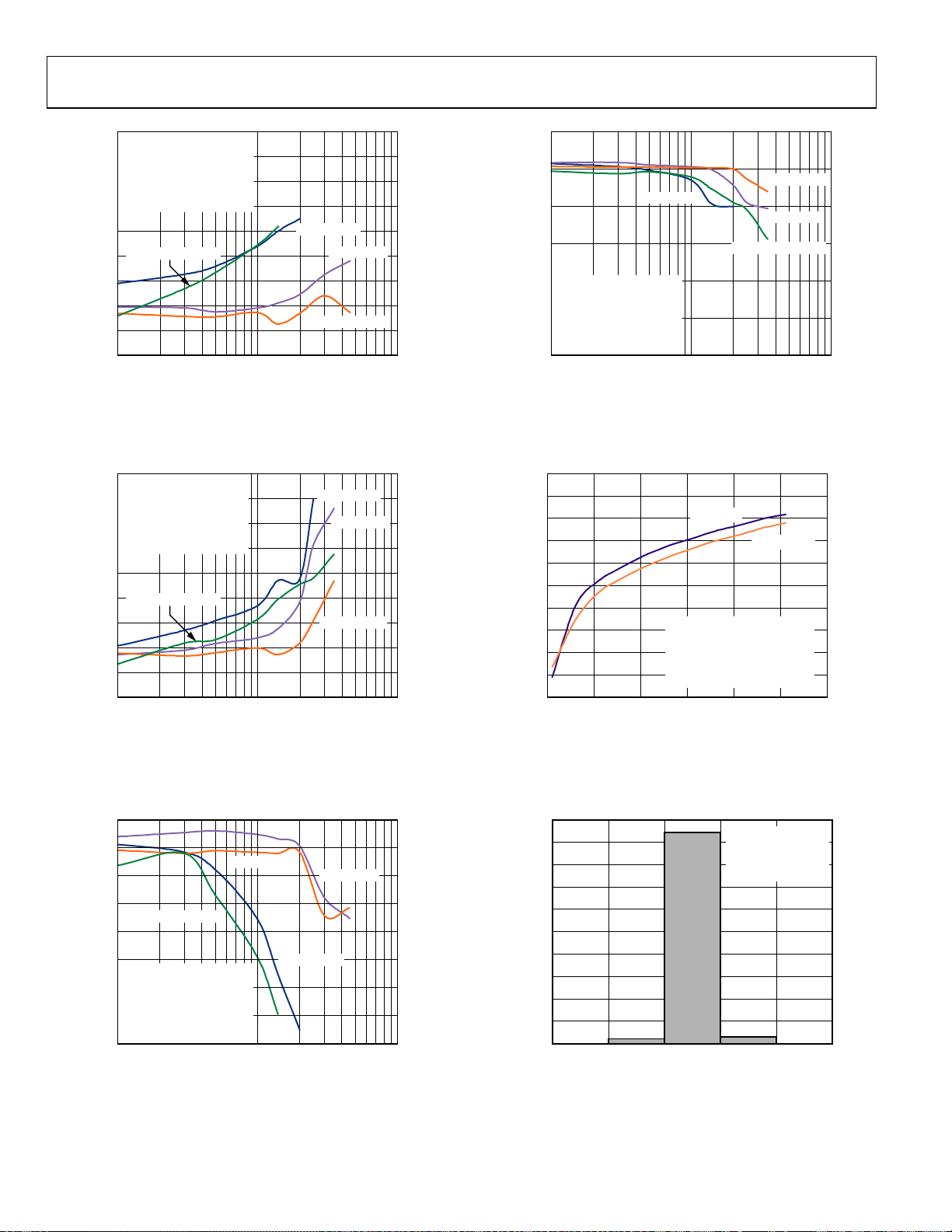
Figure 10. THD vs. Analog Input Frequency for Single-Ended Mode (SE) at 5 V V
50
VCC= V
V
DD
–55
T
A
f
= 1MSPS
S
–60
INTERNAL REFERENCE
AD8021 BETWEEN MUX
AND ADCIN PINS
–65
–70
–75
0V TO +10V RANG E
THD (dB)
–80
–85
–90
–95
10
= 5V
DRIVE
= 12V, VSS = –12V
= 25°C
PINS
IN+
ANALOG INPUT FREQUENCY (kHz)
= 5V
DRIVE
= 12V, VSS = –12V
= 25°C
ANALOG INPUT FREQUENCY (kHz)
OUT+
OUT
100
100
±10V RANGE
±5V RANGE
±2.5V RANGE
±10V RANGE
±5V RANGE
±2.5V RANGE
1000
1000
05402-010
CC
05402-011
Figure 11. THD vs. Analog Input Frequency for True Differential Mode (Diff) at
5 V V
CC
80
75
70
65
SINAD (dB)
60
VCC= V
DRIVE
= 12V, VSS = –12V
V
DD
= 25°C
T
A
f
= 1MSPS
S
55
INTERNAL REFERENCE
AD8021 BETWEEN MUX
AND ADCIN PINS
50
10
Figure 13. SINAD vs. Analog Input Frequency for True Differential Mode (Diff)
50
–55
–60
–65
–70
–75
–80
–85
–90
CHANNEL-TO -CHANNEL ISO LATION (dB)
–95
–100
0
100 200 300 400 500
±10V RANGE
= 5V
OUT
100
ANALOG INPUT FREQUENCY (kHz)
at 5 V V
CC
WIRE LINK
VDD = 12V, VSS = –12V
= V
V
CC
DRIVE
SINGLE-E NDED MODE
50kHz ON SELECT ED CHANNE L
f
= 1MSPS
S
= 25°C
T
A
FREQUENCY O F INPUT NO ISE (kHz)
±2.5V RANGE
±5V RANGE
0V TO +10V RANG E
WITH AD8021
= 5V
1000
600
05402-013
05402-014
Figure 14. Channel-to-Channel Isolation with and Without AD8021 Between
the MUX
+ and ADCIN + Pins
OUT
74
73
72
71
0V TO +10V RANG E
70
SINAD (dB)
69
VCC= V
= 12V, VSS = –12V
V
DD
68
= 25°C
T
A
f
= 1MSPS
S
INTERNAL REFERENCE
67
AD8021 BETWEEN MUX
AND ADC
66
10
= 5V
DRIVE
PINS
IN+
ANALOG INPUT FREQUENCY (kHz)
±2.5V RANGE
OUT+
100
±5V RANGE
±10V RANGE
1000
05402-012
Figure 12. SINAD vs. Analog Input Frequency for Single-Ended Mode (SE) at 5 V V
CC
10k
9k
8k
7k
6k
5k
4k
3k
NUMBER OF OCCURRENCES
2k
1k
0
0
–2
228
–1012
9469
CODE
VCC = 5V
= 12V, VSS = –12V
V
DD
RANGE = ±10V
10k SAMPLES
= 25°C
T
A
303
Figure 15. Histogram of Codes, True Differential Mode
0
05402-015
Rev. 0 | Page 12 of 40
Page 13

AD7329
–
–
–
8k
7k
6k
5k
4k
3k
2k
NUMBER OF OCCURRENCES
1k
023
0
–3
–2 –1 0 1 2 3
1201
7600
CODE
VCC = 5V
= 12V, VSS = –12V
V
DD
RANGE = ±10V
10k SAMPLES
= 25°C
T
A
1165
Figure 16. Histogram of Codes, Single-Ended Mode
50
–55
–60
–65
VCC = 5V
–70
–75
CMRR (dB)
–80
–85
–90
–95
–100
0
= 3V
V
CC
DIFFERENTIAL MODE
f
= 50kHz
IN
V
= 12V, VSS = –12V
DD
f
= 1MSPS
S
= 25°C
T
A
200 400 600 800 1000 1200
RIPPLE FREQUENCY (kHz)
Figure 17. CMRR vs. Common-Mode Ripple Frequency
11 0
05402-016
05402-017
2.0
1.5
1.0
0.5
0
–0.5
INL ERROR (LSB)
–1.0
–1.5
–2.0
±5 ±7 ±9 ±11 ±13 ±15 ±17 ±19
INL = 500kSPS
INL = 1MSPS
SUPPLY VOLTAGE (V) (V
INL = 1MSPS
INL = 500kSPS
±5V RANGE
V
= V
DRIVE
= +, VSS= –)
DD
+ PINS
IN
= 5V
CC
INTERNAL REFERENCE
SINGLE-E NDED MODE
AD8021 BETWEEN MUX
AND ADC
OUT
+
Figure 19. INL Error vs. Supply Voltage at 500 kSPS and 1 MSPS
50
100mV p-p SI NE WAVE ON EACH SUPPLY
–55
NO DECOUPLING
SINGLE-E NDED MODE
f
= 1MSPS
S
–60
–65
–70
–75
PSRR (dB)
–80
–85
–90
–95
–100
0 1200
200 400 600 800 1000
SUPPLY RIPPLE FREQ UENCY (kHz)
VCC = 3V
VDD = 12V
VCC = 5V
VSS = –12V
Figure 20. PSRR vs. Supply Ripple Frequency Without Supply Decoupling
05402-019
05402-020
2.0
1.5
1.0
0.5
0
DNL = 1MSPS
–0.5
DNL ERROR (LSB)
–1.0
–1.5
–2.0
±5 ±7 ±9 ±11 ±13 ±15 ±17 ±19
DNL = 500kSPS
SUPPLY VOLTAGE (V) (V
DNL = 500kSPS
DNL = 1MSPS
±5V RANGE
V
= V
DRIVE
= +, VSS= –)
DD
+ PINS
IN
= 5V
CC
INTERNAL REFERENCE
SINGLE-E NDED MODE
AD8021 BETWEEN MUX
AND ADC
OUT
Figure 18. DNL Error vs. Supply Voltage at 500 kSPS and 1 MSPS
+
05402-018
50
DIFFERENTIAL MODE
V
= 12V, VSS = –12V
DD
–55
V
= V
CC
INTERNAL REFERENCE
–60
AD8021 BETWEEN MUX
AND ADCIN PINS
–65
–70
–75
THD (dB)
–80
–85
–90
–95
–100
10
= 5V
DRIVE
OUT
100
ANALOG INPUT FREQUENCY (kHz)
±10V RANGE
RIN = 2000Ω
R
= 1000Ω
IN
R
= 600Ω
IN
R
= 100Ω
IN
R
= 50Ω
IN
±2.5V RANGE
RIN = 4000Ω
R
= 1000Ω
IN
R
= 600Ω
IN
R
= 100Ω
IN
R
= 50Ω
IN
1000
05402-021
Figure 21. THD vs. Analog Input Frequency for Various Source Impedances,
True Differential Mode
Rev. 0 | Page 13 of 40
Page 14

AD7329
–
–
50
SINGLE-E NDED MODE
V
= 12V, VSS = –12V
DD
–55
V
= V
CC
INTERNAL REFERENCE
AD8021 BETWEEN MUX
–60
AND ADC
–65
–70
THD (dB)
–75
–80
–85
–90
10
= 5V
DRIVE
+
+ PINS
IN
ANALOG INPUT FREQUENCY (kHz)
OUT
100
±10V RANGE
RIN = 2000Ω
R
= 1000Ω
IN
R
= 600Ω
IN
R
= 100Ω
IN
R
= 50Ω
IN
±2.5V RANGE
RIN = 2000Ω
R
= 1000Ω
IN
R
= 600Ω
IN
R
= 100Ω
IN
R
= 50Ω
IN
1000
Figure 22. THD vs. Analog Input Frequency for Various Source Impedances,
Single-Ended Mode
76
–78
–80
–82
THD (dB)
–84
–86
05402-022
10kHz/500kSPS
–88
±7 ±9 ±11 ±13 ±15
±5 ±17
30kHz/500kSPS
SUPPLY VOLTAGE (V) (VDD= +, VSS=–)
±5V RANGE
V
= V
DRIVE
+ PINS
IN
= 5V
CC
INTERNAL REFERENCE
SINGLE- ENDED MODE
AD8021 BETWEEN MUX
AND ADC
30kHz/1MSPS
10kHz/1MSPS
OUT
+
05402-055
Figure 23. THD vs. Supply Voltage at 500 kSPS and 1 MSPS
with 10 kHz and 30 kHz Input Tone
Rev. 0 | Page 14 of 40
Page 15

AD7329
TERMINOLOGY
Differential Nonlinearity
This is the difference between the measured and the ideal 1 LSB
change between any two adjacent codes in the ADC.
Integral Nonlinearity
This is the maximum deviation from a straight line passing
through the endpoints of the ADC transfer function. The
endpoints of the transfer function are zero scale (a point 1 LSB
below the first code transition) and full scale (a point 1 LSB
above the last code transition).
Negative Full-Scale Error
This applies when using twos complement output coding and
any of the bipolar analog input ranges. This is the deviation of
the first code transition (10 … 000) to (10 … 001) from the ideal
(that is, −4 × V
+ 1 LSB, −2 × V
REF
+ 1 LSB, −V
REF
+ 1 LSB)
REF
after adjusting for the bipolar zero code error.
Negative Full-Scale Error Match
This is the difference in negative full-scale error between any
two input channels.
Offset Code Error
This applies to straight binary output coding. It is the deviation
of the first code transition (00 ... 000) to (00 ... 001) from the
ideal, that is, AGND + 1 LSB.
Offset Error Match
This is the difference in offset error between any two input
channels.
Gain Error
This applies to straight binary output coding. It is the deviation
of the last code transition (111 ... 110) to (111 ... 111) from the
ideal (that is, 4 × V
− 1 LSB, 2 × V
REF
− 1 LSB, V
REF
− 1 LSB)
REF
after adjusting for the offset error.
Gain Error Match
This is the difference in gain error between any two input
channels.
Bipolar Zero Code Error
This applies when using twos complement output coding and a
bipolar analog input. It is the deviation of the midscale transition
(all 1s to all 0s) from the ideal input voltage, that is, AGND − 1 LSB.
Bipolar Zero Code Error Match
This refers to the difference in bipolar zero code error between
any two input channels.
Positive Full-Scale Error
This applies when using twos complement output coding and
any of the bipolar analog input ranges. It is the deviation of the
last code transition (011 … 110) to (011 … 111) from the ideal
(4 × V
− 1 LSB, 2 × V
REF
− 1 LSB, V
REF
− 1 LSB) after
REF
adjusting for the bipolar zero code error.
Positive Full-Scale Error Match
This is the difference in positive full-scale error between any
two input channels.
Track-and-Hold Acquisition Time
The track-and-hold amplifier returns into track mode after the
th
SCLK rising edge. Track-and-hold acquisition time is the
14
time required for the output of the track-and-hold amplifier to
reach its final value, within ±½ LSB, after the end of a conversion.
Signal to (Noise + Distortion) Ratio
This is the measured ratio of signal to (noise + distortion) at
the output of the A/D converter. The signal is the rms amplitude
of the fundamental. Noise is the sum of all nonfundamental
signals up to half the sampling frequency (f
/2), excluding dc.
S
The ratio is dependent on the number of quantization levels in
the digitization process. The more levels, the smaller the quantization noise. Theoretically, the signal to (noise + distortion) ratio
for an ideal N-bit converter with a sine wave input is given by
Signal to (Noise + Distortion) = (6.02 N + 1.76) dB
For a 13-bit converter, this is 80.02 dB.
Total Harmonic Distortion
Total harmonic distortion (THD) is the ratio of the rms sum of
harmonics to the fundamental. For the AD7329, it is defined as
2
THD
where V
, V5, and V6 are the rms amplitudes of the second through the
V
4
=
is the rms amplitude of the fundamental, and V2, V3,
1
2
log20)dB(
4
3
V
1
++++
VVVVV
5
6
2
2
2
2
sixth harmonics.
Peak Harmonic or Spurious Noise
Peak harmonic or spurious noise is defined as the ratio of the
rms value of the next largest component in the ADC output
spectrum (up to f
/2, excluding dc) to the rms value of
S
the fundamental. Normally, the value of this specification is
determined by the largest harmonic in the spectrum, but for
ADCs where the harmonics are buried in the noise floor, the
largest harmonic could be a noise peak.
Rev. 0 | Page 15 of 40
Page 16

AD7329
Channel-to-Channel Isolation
Channel-to-channel isolation is a measure of the level of crosstalk
between any two channels. It is measured by applying a full-scale,
100 kHz sine wave signal to all unselected input channels and
determining the degree to which the signal attenuates in the
selected channel with a 50 kHz signal.
worst-case across all eight channels for the AD7329. The analog
input range is programmed to be ±2.5 V on the selected channel
and ±10 V on all other channels.
Intermodulation Distortion
With inputs consisting of sine waves at two frequencies, fa and
fb, any active device with nonlinearities creates distortion
products at sum and difference frequencies of mfa ± nfb, where
m, n = 0, 1, 2, 3, and so on. Intermodulation distortion terms
are those for which neither m nor n are equal to 0. For example,
the second-order terms include (fa + fb) and (fa − fb), whereas
the third-order terms include (2fa + fb), (2fa − fb), (fa + 2fb),
and (fa − 2fb).
The AD7329 is tested using the CCIF standard where two input
frequencies near the top end of the input bandwidth are used.
In this case, the second-order terms are usually distanced in
frequency from the original sine waves, whereas the third-order
Figure 14 shows the
terms are usually at a frequency close to the input frequencies.
As a result, the second- and third-order terms are specified
separately. The calculation of the intermodulation distortion is
per the THD specification, where it is the ratio of the rms sum
of the individual distortion products to the rms amplitude of
the sum of the fundamentals expressed in decibels.
PSR (Power Supply Rejection)
Variations in power supply affect the full-scale transition but
not the linearity of the converter. Power supply rejection is the
maximum change in the full-scale transition point due to a
change in power supply voltage from the nominal value (see the
Typical Performance Characteristics section).
CMRR (Common-Mode Rejection Ratio)
CMRR is defined as the ratio of the power in the ADC output at
full-scale frequency, f, to the power of a 100 mV sine wave
applied to the common-mode voltage of the V
frequency, f
, as
S
CMRR (dB) = 10 log (Pf/Pf
)
S
+ and VIN−
IN
where Pf is the power at frequency f in the ADC output, and Pf
is the power at frequency f
in the ADC output (see Figure 17).
S
S
Rev. 0 | Page 16 of 40
Page 17

AD7329
V
V
THEORY OF OPERATION
CIRCUIT INFORMATION
The AD7329 is a fast, 8-channel, 12-bit plus sign, bipolar input,
serial A/D converter. The AD7329 can accept bipolar input ranges
that include ±10 V, ±5 V, and ±2.5 V; it can also accept a 0 V to
+10 V unipolar input range. A different analog input range can
be programmed on each analog input channel via the on-chip
registers. The AD7329 has a high speed serial interface that can
operate at throughput rates up to 1 MSPS.
The AD7329 requires V
voltage analog input structures. These supplies must be equal to
or greater than the analog input range. See
requirements of these supplies for each analog input range. The
AD7329 requires a low voltage 2.7 V to 5.25 V V
power the ADC core.
Table 6. Reference and Supply Requirements for Each
Analog Input Range
Selected
Analog
Input
Range (V)
Reference
Voltage (V)
±10 2.5 ±10 3/5 ±10
3.0 ±12 3/5 ±12
±5 2.5 ±5 3/5 ±5
3.0 ±6 3/5 ±6
±2.5 2.5 ±2.5 3/5 ±5
3.0 ±3 3/5 ±5
0 to +10 2.5 0 to +10 3/5 +10/AGND
3.0 0 to +12 3/5 +12/AGND
In order to meet the specified performance specifications when
the AD7329 is configured with the minimum V
supplies for a chosen analog input range, the throughput rate
should be decreased from the maximum throughput range (see
Typical Performance Characteristics section).
the
The analog inputs can be configured as either eight single-ended
inputs, four true differential input pairs, four pseudo differential
inputs, or seven pseudo differential inputs. Selection can be made
by programming the mode bits, Mode 0 and Mode 1, in the
control register.
The serial clock input accesses data from the part and provides
the clock source for the successive approximation ADC. The
AD7329 has an on-chip 2.5 V reference. However, the AD7329
can also work with an external reference. On power-up, the
and VSS dual supplies for the high
DD
Tabl e 6 f or t he
supply to
CC
Full-Scale
(V)
DD
Minimum
V
DD/VSS
and VSS
Input
Range (V)
AV
CC
(V)
external reference operation is the default option. If the internal
reference is the preferred option, the user must write to the
reference bit in the control register to select the internal
reference operation.
The AD7329 also features power-down options to allow power
savings between conversions. The power-down modes are
selected by programming the on-chip control register as
described in the
Modes of Operation section.
CONVERTER OPERATION
The AD7329 is a successive approximation analog-to-digital
converter built around two capacitive DACs.
Figure 25 show simplified schematics of the ADC in singleended mode during the acquisition and conversion phases,
respectively.
Figure 26 and Figure 27 show simplified schematics
of the ADC in differential mode during acquisition and
conversion phases, respectively. In both examples, the
MUX
MUX
+ pin is connected to the ADCIN+ pin, and the
OUT
− pin is connected to the ADCIN− pin. The ADC is
OUT
composed of control logic, a SAR, and capacitive DACs. In
Figure 24 (the acquisition phase), SW2 is closed and SW1 is in
Position A, the comparator is held in a balanced condition, and
the sampling capacitor array acquires the signal on the input.
C
S
B
0
IN
A
SW1
AGND
Figure 24. ADC Acquisition Phase (Single Ended)
COMPARATOR
SW2
When the ADC starts a conversion (Figure 25), SW2 opens and
SW1 moves to Position B, causing the comparator to become
unbalanced. The control logic and the charge redistribution
DAC are used to add and subtract fixed amounts of charge from
the capacitive DAC to bring the comparator back into a
balanced condition. When the comparator is rebalanced, the
conversion is complete. The control logic generates the ADC
output code
C
S
B
0
IN
A
AGND
Figure 25. ADC Conversion Phase (Single Ended)
COMPARATOR
SW2SW1
Figure 24 and
CAPACITIVE
DAC
CONTROL
LOGIC
CAPACITIVE
DAC
CONTROL
LOGIC
05402-023
05402-024
Rev. 0 | Page 17 of 40
Page 18

AD7329
V
V
V
V
V
V
Figure 26 shows the differential configuration during the
acquisition phase. For the conversion phase, SW3 opens and
SW1 and SW2 move to Position B (see
impedances of the source driving the V
match; otherwise, the two inputs have different settling times,
resulting in errors.
C
S
B
+
IN
A
SW1
SW2
A
–
IN
B
V
REF
SW3
C
S
Figure 26. ADC Differential Configuration During Acquisition Phase
Figure 27). The output
+ and VIN− pins must
IN
CAPACITIVE
COMPARATOR
CONTROL
CAPACITIVE
DAC
LOGIC
DAC
05402-025
The ideal transfer characteristic for the AD7329 when twos
complement coding is selected is shown in
Figure 28. The ideal
transfer characteristic for the AD7329 when straight binary
coding is selected is shown in
011 ... 111
011 ... 110
000 ... 001
000 ... 000
111 . .. 111
ADC CODE
100 ... 010
100 ... 001
100 ... 000
–FSR/2 + 1L SB
AGND + 1LSB
Figure 28. Twos Complement Transfer Characteristic (Bipolar Ranges)
AGND – 1LSB
Figure 29.
+FSR/2 – 1LSB BIPOLAR RANG ES
+FSR – 1LSB UNI POLAR RANGE
ANALOG INPUT
05402-027
CAPACITIVE
DAC
C
S
B
+
IN
A
SW1
SW2
A
–
IN
B
C
S
V
REF
COMPARATOR
SW3
CONTROL
LOGIC
CAPACITIVE
DAC
05402-026
Figure 27. ADC Differential Configuration During Conversion Phase
OUTPUT CODING
The AD7329 default output coding is set to twos complement.
The output coding is controlled by the coding bit in the control
register. To change the output coding to straight binary coding,
the coding bit in the control register must be set. When
operating in sequence mode, the output coding for each
channel in the sequence is the value written to the coding bit
during the last write to the control register.
TRANSFER FUNCTIONS
The designed code transitions occur at successive integer LSB
values (that is, 1 LSB, 2 LSB, and so on). The LSB size is
dependent on the analog input range selected.
Table 7. LSB Sizes for Each Analog Input Range
Input Range Full-Scale Range/8192 Codes LSB Size
±10 V 20 V 2.441 mV
±5 V 10 V 1.22 mV
±2.5 V 5 V 0.61 mV
0 V to +10 V 10 V 1.22 mV
111 .. . 111
111 .. . 11 0
111 ... 000
011 ... 111
ADC CODE
000 ... 010
000 ... 001
000 ... 000
–FSR/2 + 1L SB
AGND + 1LSB
+FSR/2 – 1LSB BIPOLAR RANG ES
+FSR – 1LSB UNI POLAR RANGE
ANALOG INPUT
05402-028
Figure 29. Straight Binary Transfer Characteristic (Bipolar Ranges)
ANALOG INPUT STRUCTURE
The analog inputs of the AD7329 can be configured as singleended, true differential, or pseudo differential via the control
register mode bits, as shown in
The AD7329 can accept true bipolar input signals. On powerup, the analog inputs operate as eight single-ended analog input
channels. If true differential or pseudo differential is required, a
write to the control register is necessary after power-up to
change this configuration.
Figure 30 shows the equivalent analog input circuit of the
AD7329 in single-ended mode.
analog input structure in differential mode. The two diodes
provide ESD protection for the analog inputs.
DD
0
IN
Figure 30. Equivalent Analog Input Circuit (Single Ended)
D
C1 C3 C4
D
V
SS
Table 4 of the Registers section.
Figure 31 shows the equivalent
ADCIN+MUX
+
OUT
C2
R1
05402-029
Rev. 0 | Page 18 of 40
Page 19

AD7329
V
V
V
DD
+
IN
C1 C3 C4
V
SS
V
DD
–
IN
C1 C3 C4
V
SS
D
D
D
D
OUT
OUT
ADCIN+MUX
+
C2
R1
ADCIN–MUX
–
C2
R1
05402-030
Figure 31. Equivalent Analog Input Circuit (Differential)
Care should be taken to ensure that the analog input does not
exceed the V
and VSS supply rails by more than 300 mV.
DD
Exceeding this value causes the diodes to become forward
biased and to start conducting into either the V
supply rail. These diodes can conduct up to 10 mA
the V
SS
supply rail or
DD
without causing irreversible damage to the part.
Figure 30 and Figure 31, Capacitor C1 is typically 4 pF and
In
can primarily be attributed to pin capacitance. Resistor R1 is a
lumped component made up of the on resistance of the input
multiplexer and the track-and-hold switch. Capacitor C2 is the
sampling capacitor; its capacitance varies depending on the
analog input range selected (see the
Specifications section).
TRACK-AND-HOLD SECTION
The track-and-hold on the analog input of the AD7329 allows
the ADC to accurately convert an input sine wave of full-scale
amplitude to 13-bit accuracy. The input bandwidth of the trackand-hold is greater than the Nyquist rate of the ADC. The
AD7329 can handle frequencies up to 20 MHz.
The ADC
and-hold circuit. This is a high impedance input. Connecting
the MUX
multiplexer output to the track-and-hold circuit. The input
voltage range on the ADC
register bits for the input channel selected. The user must
ensure that the input voltage to the ADC
selected voltage range.
The track-and-hold enters its tracking mode on the 14
rising edge after the
acquire an input signal depends on how quickly the sampling
capacitor is charged. With zero source impedance, 300 ns is
sufficient to acquire the signal to the 13-bit level.
The acquisition time required is calculated using the following
formula:
pins connect directly to the input stage of the track-
IN
pins directly to the ADCIN pins connects the
OUT
pins is determined by the range
IN
pins is within the
IN
CS
falling edge. The time required to
= 10 × ((R
t
ACQ
SOURCE
+ R)C)
th
SCLK
For the AD7329, the value of R includes the on resistance of the
input multiplexer. The value of R is typically 300 Ω. R
SOURCE
should include any extra source impedance on the analog input.
th
The AD7329 enters track mode on the 14
SCLK rising edge.
When the AD7329 is run at a throughput rate of 1 MSPS with a
20 MHz SCLK signal, the ADC has approximately 1.5 SCLK
periods plus t
plus the quiet time, t
8
input signal. The ADC goes back into hold mode on the
, to acquire the analog
QUIET
CS
falling edge.
The current required to drive the ADC is extremely small when
using the external op amp between the MUX
and ADC
OUT
IN
pins. This is due to the high input impedance of the op amp
placed between the MUX
Figure 32, where the current required to drive the AD7329
in
input is <0.2 A when
and ADC
pins.
IN
0.20
0.19
0.18
0.17
0.16
INPUT CURRENT (µ A)
0.15
0.14
100 200 300 400 500 600 700 800 900
0
and ADC
OUT
AD8021 is placed between the MUX
VDD = 12V, VSS = –12V
V
SINGLE-E NDED MODE
50kHz ON SELECT ED CHANNE L
f
T
AD8021 BETWEEN MUX
AND ADCIN PINS
THROUGHPUT RATE (kSPS)
Figure 32. Input Current vs. Throughput Rate
AD8021 Between MUX
with
35
30
25
20
15
INPUT CURRENT (µ A)
10
5
0
100 200 300 400 500 600 700 800 900
0
THROUGHPUT RATE (kSPS)
VDD = 12V, VSS = –12V
V
SINGLE-E NDED MODE
50kHz ON SELECT ED CHANNE L
f
T
WIRE LINK BETWEEN MUX
AND ADCIN PINS
Figure 33. Input Current vs. Throughput Rate
with a Wire Link Between MUX
pins. This can be seen
IN
= V
= V
= 5V
DRIVE
and ADCIN
OUT
= 5V
DRIVE
and ADCIN
OUT
CC
= 50kHz
IN
= 25°C
A
CC
= 50kHz
IN
= 25°C
A
OUT
OUT
1000
1000
OUT
05402-056
05402-057
where C is the sampling capacitance, and R is the resistance
seen by the track-and-hold amplifier looking at the input.
Rev. 0 | Page 19 of 40
Page 20

AD7329
+
–
V
+15V
V
V
V
TYPICAL CONNECTION DIAGRAM
Figure 34 shows a typical connection diagram for the AD7329.
In this configuration, the AGND pin is connected to the analog
ground plane of the system, and the DGND pin is connected to
the digital ground plane of the system. The analog inputs on the
AD7329 can be configured to operate in single-ended, true
differential, or pseudo differential mode. The AD7329 can operate
with either an internal or external reference. In
AD7329 is configured to operate with the internal 2.5 V reference.
A 680 nF decoupling capacitor is required when operating with
the internal reference.
The V
voltage. The V
pin can be connected to either a 3 V or a 5 V supply
CC
and VSS are the dual supplies for the high
DD
voltage analog input structures. The voltage on these pins must
be equal to or greater than the highest analog input range
selected on the analog input channels (see
information). The V
pin is connected to the supply voltage
DRIVE
of the microprocessor. The voltage applied to the V
controls the voltage of the serial interface.
FILTERING/BUFFERING
15V
ANALOG INP UTS
±10V, ±5V, ±2.5V
0V TO +10V
15V
ANALOG INP UTS
±10V, ±5V, ±2.5V
0V TO +10V
–15V
680nF
+
10µF0.1µF
1
+
MUX
ADC
OUT
AD7329
OUT
–
1
MUX
ADC
OUT
SS
1
MINIMUM VDDAND VSS SUPPLY VOLTAGES
DEPEND ON THE HIGHEST ANALOG INPUT
RANGE SELECTED.
VIN0
VIN1
VIN2
VIN3
VIN4
VIN5
VIN6
VIN7
REFIN/REF
10µF0.1µF
+
V
DD
V
+
IN
–
IN
10µF 0.1µF
V
CC
V
DRIVE
CS
DOUT
SCLK
DIN
DGND
AGND
Figure 34. Typical Connection Diagram (Single-Ended Mode)
FILTERING/BUFFERING
680nF
+
10µF0.1µF
10µF0.1µF
+
1
–
+
V
DD
OUT
OUT
MUX
MUX
VIN0
VIN1
VIN2
VIN3
VIN4
VIN5
VIN6
VIN7
REFIN/REF
AD7329
OUT
1
V
SS
1
MINIMUM VDDAND VSS SUPPLY VOLTAGES
DEPEND ON THE HIGHEST ANALOG INPUT
RANGE SELECTED.
–
ADC
IN
+
ADC
IN
V
V
CC
DRIVE
DOUT
SCLK
DGND
AGND
10µF 0. 1µF
CS
DIN
Figure 35. Typical Connection Diagram (Differential Mode)
Figure 34, the
Tabl e 6 f or m o re
DRIVE
INTERFACE
+
+3V SUPPLY
SERIAL
+3V SUPPLY
SERIAL
INTERFACE
VCC +2.7V TO +5.25
VCC +2.7V TO +5.25
+
+
10µF 0. 1µF
+
10µF 0.1µ F
input
µC/µP
µC/µP
ANALOG INPUT
Single-Ended Inputs
The AD7329 has a total of eight analog inputs when operating
in single-ended mode. Each analog input can be independently
programmed to one of the four analog input ranges. In applications
where the signal source is high impedance, it is recommended
to buffer the signal before applying it to the ADC analog inputs.
Figure 36 shows the configuration of the AD7329 in singleended mode.
+
AGND
+
V
IN
AD7329
V–
1
ADDITIONAL PI NS OMIT TED FOR CL ARITY.
Figure 36. Single-Ended Mode Typical Connection Diagram
True Differential Mode
The AD7329 can have four true differential analog input pairs.
Differential signals have some benefits over single-ended
signals, including better noise immunity based on the device’s
common-mode rejection and improvements in distortion
performance.
Figure 37 defines the configuration of the true
differential analog inputs of the AD7329.
+
V
IN
1
AD7329
–
V
IN
1
05402-031
ADDITIONAL PINS OMITTED FOR CLARITY.
Figure 37. True Differential Inputs
The amplitude of the differential signal is the difference
between the signals applied to the V
each differential pair (V
+ − VIN−). VIN+ and VIN− should
IN
+ and VIN− pins in
IN
be simultaneously driven by two signals of equal amplitude,
dependent on the input range selected, that are 180° out of
phase. Assuming the ±4 × V
mode, the amplitude of the
REF
differential signal is −20 V to +20 V p-p (2 × 4 × V
regardless of the common mode.
The common mode is the average of the two signals
+ + VIN−)/2
(V
IN
and is therefore the voltage on which the two input signals are
centered.
05402-032
5
V
V
DD
CC
1
V
SS
5402-033
05402-034
),
REF
Rev. 0 | Page 20 of 40
Page 21

AD7329
This voltage is set up externally, and its range varies with
reference voltage. As the reference voltage increases, the
common-mode range decreases. When driving the differential
inputs with an amplifier, the actual common-mode range is
determined by the amplifier’s output swing. If the differential
inputs are not driven from an amplifier, the common-mode
range is determined by the supply voltage on the V
and the V
supply pin.
SS
supply pin
DD
When a conversion takes place, the common mode is rejected,
resulting in a noise-free signal of amplitude −2 × (4 × V
(4 × V
), corresponding to Digital Codes −4096 to +4095.
REF
5
4
3
2
1
0
RANGE (V)
–1
COM
–2
V
–3
–4
VCC = 3V
–5
V
REF
–6
Figure 38. Common-Mode Range for V
8
6
4
= 3V
±10V
RANGE
±10V
RANGE
±5V RANGE
±16.5V VDD/V
±5V RANGE
±2.5V
RANGE
±10V
RANGE
±12V VDD/V
SS
= 3 V and REFIN/REF
CC
±2.5V
RANGE
±5V RANGE
±5V RANGE
) to +2 ×
REF
±2.5V
RANGE
OUT
±2.5V
= 3 V
05402-035
SS
RANGE
6
4
2
0
RANGE (V)
–2
COM
V
–4
–6
VCC = 3V
V
REF
–8
RANGE
= 2.5V
±5V RANGE
±10V
±16.5V VDD/V
±2.5V
RANGE
SS
±5V RANGE
±10V
RANGE
±12V VDD/V
±2.5V
RANGE
SS
Figure 40. Common-Mode Range for VCC = 3 V and REFIN/REF
8
±2.5V
RANGE
SS
VCC = 5V
V
= 2.5V
REF
±10V
RANGE
±5V RANGE
±16.5V VDD/V
6
4
2
0
RANGE (V)
–2
COM
V
–4
–6
–8
Figure 41. Common-Mode Range for V
CC
±5V RANGE
±10V
RANGE
±12V VDD/V
SS
= 5 V and REFIN/REF
OUT
±2.5V
RANGE
OUT
05402-037
= 2.5 V
= 2.5 V
05402-038
2
RANGE (V)
COM
V
0
–2
VCC = 5V
V
= 3V
REF
–4
±16.5V VDD/V
SS
Figure 39. Common-Mode Range for V
±10V
RANGE
±12V VDD/V
= 5 V and REFIN/REF
CC
SS
05402-036
= 3 V
OUT
Rev. 0 | Page 21 of 40
Page 22

AD7329
V
V
–
–2–4–
Pseudo Differential Inputs
The AD7329 can have four pseudo differential pairs or seven
pseudo differential inputs referenced to a common V
+ inputs are coupled to the signal source and must have
The V
IN
− pin.
IN
an amplitude within the selected range for that channel, as
programmed in the range register. A dc input is applied to the
− pin. The voltage applied to this input provides an offset for
V
IN
+ input from ground or pseudo ground. Pseudo differential
the V
IN
inputs separate the analog input signal ground from the ADC
ground, allowing cancellation of dc common-mode voltages.
Figure 42 shows the configuration of the AD7329 in pseudo
differential mode.
When a conversion takes place, the pseudo ground corresponds
to Code −4096 and the maximum amplitude corresponds to
Code +4095.
+
V
+
IN
AD7329
VIN–
V–
1
ADDITIONAL PI NS OMIT TED FOR CL ARITY.
Figure 42. Pseudo Differential Inputs
5
V
V
DD
CC
1
V
SS
5402-039
Figure 43 and Figure 44 show the typical voltage range on the
− pin for various analog input ranges when configured in
V
IN
the pseudo differential mode.
8
6
4
2
0
–2
–4
–6
–8
VCC = 5V
V
REF
±10V
RANGE
= 2.5V
±5V RANGE
±16.5V VDD/V
±2.5V
RANGE
Figure 43. Pseudo Input Range with V
4
REF
±10V
RANGE
= 2.5V
±5V RANGE
±2.5V
RANGE
±16.5V V
DD/VSS
2
0
6
8
VCC = 3V
V
Figure 44. Pseudo Input Range with V
0V TO +10V
RANGE
SS
0V TO +10V
RANGE
±5V RANGE
±10V
RANGE
±12V VDD/V
±5V RANGE
±10V
RANGE
±12V VDD/V
±2.5V
RANGE
0V TO +10V
RANGE
SS
= 5 V
CC
±2.5V
RANGE
0V TO +10V
RANGE
SS
= 3 V
CC
05402-040
05402-041
For example, when the AD7329 is configured to operate in
pseudo differential mode and the ±5 V range is selected with
16.5 V V
, −16.5 V VSS, and 5 V VCC, the voltage on the VIN−
DD
pin can vary from −6.5 V to +6.5 V.
Rev. 0 | Page 22 of 40
Page 23

AD7329
DRIVER AMPLIFIER CHOICE
In applications where the harmonic distortion and signal-tonoise ratio are critical specifications, the analog input of the
AD7329 should be driven from a low impedance source. Large
source impedances significantly affect the ac performance of the
ADC and can necessitate the use of an input buffer amplifier.
When no amplifier is used to drive the analog input, the source
impedance should be limited to low values. The maximum
source impedance depends on the amount of THD that can be
tolerated in the application. The THD increases as the source
impedance increases and performance degrades.
Figure 22 show graphs of the THD vs. the analog input
frequency for various source impedances. Depending on the
input range and analog input configuration selected, the
AD7329 can handle source impedances of up to 4 kΩ before the
THD starts to degrade.
Due to the programmable nature of the analog inputs on the
AD7329, the choice of op amp used to drive the inputs is a
function of the particular application and depends on the input
configuration and the analog input voltage ranges selected.
The driver amplifier must be able to settle for a full-scale step to
a 13-bit level, 0.0122%, in less than the specified acquisition
time of the AD7329. An op amp such as the
requirement when operating in single-ended mode. The
needs an external compensating NPO type of capacitor. The
AD8022 can also be used in high frequency applications where
a dual version is required. For lower frequency applications, op
amps such as the
AD797, AD845, and AD8610 can be used with
the AD7329 in single-ended mode configuration.
Figure 21 and
AD8021 meets this
AD8021
Table 8. Typical AC Performance
Using Different Op Amps in Single-Ended Mode
No
±10 V SNR (dB)
SNRD (dB)
THD (dB)
Buffer AD845 AD8021 AD8610
74.24 74.03 73.78 73.88
72.42 74.88 72.11 71.98
−77.05 −75.95 −77.04 −76.47
Table 9. Typical AC Performance
Using Different Op Amps in Differential Mode
No
±10 V SNR (dB)
SNRD (dB)
THD (dB)
Buffer AD845 AD8021 AD8610
77.16 76.81 76.95 76.76
76.50 76.02 76.78 75.89
−84.91 −83.74 −90.55 −83.24
Differential operation requires that VIN+ and VIN− be
simultaneously driven with two signals of equal amplitude that
are 180° out of phase. The common mode must be set up
externally to the AD7329. The common-mode range is
/REF
determined by the REF
IN
voltage, the VCC supply voltage,
OUT
and the particular amplifier used to drive the analog inputs.
Differential mode with either an ac input or a dc input provides
the best THD performance over a wide frequency range. Because
not all applications have a signal preconditioned for differential
operation, there is often a need to perform a single-ended-todifferential conversion.
This single-ended-to-differential conversion can be performed
using an op amp pair. Typical connection diagrams for an op
amp pair are shown in
Figure 45 and Figure 46. In Figure 45,
the common-mode signal is applied to the noninverting input
of the second amplifier.
Rev. 0 | Page 23 of 40
Page 24

AD7329
Ω
V
V
1.5k
2kΩ
V
IN
V+
1.5kΩ
1.5kΩ
10kΩ
Figure 45. Single-Ended-to-Differential Configuration with the
1.5kΩ
1.5kΩ
V–
for Bipolar Operation
442Ω
DD
100nF
7
100nF
3
AD8021
2
6
5
4
10pF
V
SS
+
ADC
IN
05402-058
and ADCIN Pins
OUT
MUX
+
OUT
05402-042
Figure 47.
AD8021 Configuration Used Between MUX
AD845
442Ω
IN
AD8021
V+
442Ω
442Ω
442Ω
442Ω
V–
AD8021
100Ω
Figure 46. Single-Ended-to-Differential Configuration with the
05402-043
AD8021
Rev. 0 | Page 24 of 40
Page 25

AD7329
REGISTERS
The AD7329 has four programmable registers: the control register, sequence register, Range Register 1, and Range Register 2.
These registers are write-only registers.
ADDRESSING REGISTERS
A serial transfer on the AD7329 consists of 16 SCLK cycles. The three MSBs on the DIN line during the 16 SCLK transfer are decoded to
determine which register is addressed. The three MSBs consist of the write bit, Register Select 1 bit, and Register Select 2 bit. The register
select bits are used to determine which of the four on-board registers is selected. The write bit determines if the data on the DIN line
following the register select bits loads into the addressed register. If the write bit is 1, the bits load into the register addressed by the
register select bits. If the write bit is 0, the data on the DIN line does not load into any register.
Table 10. Decoding Register Select Bits and Write Bit
Write Register Select 1 Register Select 2 Description
0 0 0 Data on the DIN line during this serial transfer is ignored.
1 0 0
1 0 1
1 1 0
1 1 1
This combination selects the control register. The subsequent 12 bits are loaded into
the control register.
This combination selects Range Register 1. The subsequent 8 bits are loaded into
Range Register 1.
This combination selects Range Register 2. The subsequent 8 bits are loaded into
Range Register 2.
This combination selects the sequence register. The subsequent 8 bits are loaded into
the sequence register.
Rev. 0 | Page 25 of 40
Page 26

AD7329
CONTROL REGISTER
The control register is used to select the analog input channel, analog input configuration, reference, coding, and power mode. The
control register is a write-only, 12-bit register. Data loaded on the DIN line corresponds to the AD7329 configuration for the next
conversion. If the sequence register is being used, data should be loaded into the control register after the range registers and the sequence
register have been initialized. The bit functions of the control register are shown in
MSB LSB
15 14 13 12 11 10 9 8 7 6 5 4 3 2 1 0
Write Register
Select 1
Register
Select 2
ADD2 ADD1 ADD0 Mode 1 Mode 0 PM1 PM0 Coding Ref Seq1 Seq2 Weak/
Table 11. Control Register Details
Bit Mnemonic Description
12, 11, 10
9, 8 Mode 1, Mode 0
7, 6 PM1, PM0 The power management bits are used to select different power mode options on the AD7329 (see Table 13).
5 Coding
4 Ref
3, 2 Seq1/Seq2 The Sequence 1 and Sequence 2 bits are used to control the operation of the sequencer (see Table 14).
1
ADD2, ADD1,
ADD0
Weak/Three- State
These three channel address bits are used to select the analog input channel for the next conversion if the
sequencer is not being used. If the sequencer is being used, the three channel address bits are used to
select the final channel in a consecutive sequence.
These two mode bits are used to select the configuration of the eight analog input pins, V
pins are used in conjunction with the channel address bits. On the AD7329, the analog inputs can be
configured as eight single-ended inputs, four fully differential input pairs, four pseudo differential inputs,
or seven pseudo differential inputs (see
This bit is used to select the type of output coding the AD7329 uses for the next conversion result. If the
coding = 0, the output coding is twos complement. If the coding = 1, the output coding is straight binary.
When operating in sequence mode, the output coding for each channel is the value written to the coding
bit during the last write to the control register.
The reference bit is used to enable or disable the internal reference. If Ref = 0, the external reference is
enabled and used for the next conversion and the internal reference is disabled. If Ref = 1, the internal reference is used for the next conversion. When operating in sequence mode, the reference used for each
channel is the value written to the Ref bit during the last write to the control register.
This bit selects the state of the DOUT line at the end of the current serial transfer. If the bit is set to 1, the
DOUT line is weakly driven to Channel Address Bit ADD2 of the following conversion. If this bit is set to 0,
DOUT returns to three-state at the end of the serial transfer (see the Serial Interface section).
Table 12).
Table 11 (the power-up status of all bits is 0).
Three-State
0 to VIN7. These
IN
0
The eight analog input channels can be configured as seven pseudo differential analog inputs, four pseudo differential inputs, four true
differential input pairs, or eight single-ended analog inputs.
Table 12. Analog Input Configuration Selection
Mode 1 = 1, Mode 0 = 1 Mode 1 = 1, Mode 0 = 0 Mode 1 = 0, Mode 0 =1 Mode 1 = 0, Mode 0 = 0
Channel Address Bits 7 Pseudo Differential I/Ps 4 Fully Differential I/Ps 4 Pseudo Differential I/Ps 8 Single-Ended I/Ps
ADD2 ADD1 ADD0 VIN+ VIN− VIN+ VIN− VIN+ VIN− VIN+ VIN−
0 0 0 VIN0 VIN7 VIN0 VIN1 VIN0 VIN1 VIN0 AGND
0 0 1 VIN1 VIN7 VIN0 VIN1 VIN0 VIN1 VIN1 AGND
0 1 0 VIN2 VIN7 VIN2 VIN3 VIN2 VIN3 VIN2 AGND
0 1 1 VIN3 VIN7 VIN2 VIN3 VIN2 VIN3 VIN3 AGND
1 0 0 VIN4 VIN7 VIN4 VIN5 VIN4 VIN5 VIN4 AGND
1 0 1 VIN5 VIN7 VIN4 VIN5 VIN4 VIN5 VIN5 AGND
1 1 0 VIN6 VIN7 VIN6 VIN7 VIN6 VIN7 VIN6 AGND
1 1 1 Temperature indicator VIN6 VIN7 VIN6 VIN7 VIN7 AGND
Rev. 0 | Page 26 of 40
Page 27

AD7329
Table 13. Power Mode Selection
PM1 PM0 Description
1 1
1 0
0 1
0 0 Normal Mode. All internal circuitry is powered up at all times.
Table 14. Sequencer Selection
Seq1 Seq2 Description
0 0
0 1
1 0
1 1
Full Shutdown Mode. In this mode, all internal circuitry on the AD7329 is powered down. Information in the control register
is retained when the AD7329 is in full shutdown mode.
Autoshutdown Mode. The AD7329 enters autoshutdown on the 15
All internal circuitry is powered down in autoshutdown.
Autostandby Mode. In this mode, all internal circuitry is powered down, excluding the internal reference. The AD7329 enters
autostandby mode on the 15th SCLK rising edge after the control register is updated.
The channel sequencer is not used. The analog channel, selected by programming the ADD2 to ADD0 bits in the control
register, selects the next channel for conversion.
Uses the sequence of channels that were previously programmed in the sequence register for conversion. The AD7329
starts converting on the lowest channel in the sequence. The channels are converted in ascending order. If uninterrupted,
the AD7329 keeps converting the sequence. The range for each channel defaults to the range previously written into the
corresponding range register.
This configuration is used in conjunction with the channel address bits in the control register. This allows continuous
conversions on a consecutive sequence of channels, from Channel 0 through a final channel selected by the channel
address bits in the control register. The range for each channel defaults to the range previously written into the
corresponding range register.
The channel sequencer is not used. The analog channel, selected by programming the ADD2 bit to ADD0 bit in the control
register, selects the next channel for conversion.
th
SCLK rising edge when the control register is updated.
Rev. 0 | Page 27 of 40
Page 28

AD7329
SEQUENCE REGISTER
The sequence register on the AD7329 is an 8-bit, write-only register. Each of the eight analog input channels has one corresponding bit in
the sequence register. To select a channel for inclusion in the sequence, set the corresponding channel bit to 1 in the sequence register.
MSB LSB
16 15 14 13 12 11 10 9 8 7 6 5 4 3 2 1
Write Register Select 1 Register Select 2 VIN0 VIN1 VIN2 VIN3 VIN4 VIN5 VIN6 VIN7 0 0 0 0 0
RANGE REGISTERS
The range registers are used to select one analog input range per analog input channel. Range Register 1 is used to set the ranges for
Channel 0 to Channel 3. It is an 8-bit, write-only register with two dedicated range bits for each of the analog input channels from
Channel 0 to Channel 3. There are four analog input ranges, ±10 V, ±5 V, ±2.5 V, and 0 V to +10 V. A write to Range Register 1 is selected
by setting the write bit to 1 and the range select bits to 0 and 1. After the initial write to Range Register 1 occurs, each time an analog
input is selected, the AD7329 automatically configures the analog input to the appropriate range, as indicated by Range Register 1.
The ±10 V input range is selected by default on each analog input channel (see
MSB LSB
16 15 14 13 12 11 10 9 8 7 6 5 4 3 2 1
Write Register Select 1 Register Select 2 VIN0A VIN0B VIN1A VIN1B VIN2A VIN2B VIN3A VIN3B 0 0 0 0 0
Table 15).
Range Register 2 is used to set the ranges for Channel 4 to Channel 7. It is an 8-bit, write-only register with two dedicated range bits for
each of the analog input channels from Channel 4 to Channel 7. There are four analog input ranges, ±10 V, ±5 V, ±2.5 V, and 0 V to +10 V.
After the initial write to Range Register 2 occurs, each time an analog input is selected, the AD7329 automatically configures the analog
input to the appropriate range, as indicated by Range Register 2. The ±10 V input range is selected by default on each analog input
channel (see
MSB LSB
16 15 14 13 12 11 10 9 8 7 6 5 4 3 2 1
Write Register Select 1 Register Select 2 VIN4A VIN4B VIN5A VIN5B VIN6A VIN6B VIN7A VIN7B 0 0 0 0 0
Table 15).
Table 15. Range Selection
VINxA VINxB Description
0 0 This combination selects the ±10 V input range on VINx.
0 1 This combination selects the ±5 V input range on VINx.
1 0 This combination selects the ±2.5 V input range on VINx.
1 1 This combination selects the 0 V to +10 V input range on VINx.
Rev. 0 | Page 28 of 40
Page 29

AD7329
SEQUENCER OPERATION
POWER ON.
CS
DIN: WRITE TO RANGE REGISTER 1 TO SELECT THE RANGE
FOR EACH ANALOG INPUT CHANNEL.
DOUT: CONVERSION RESULT FROM CHANNEL 0, ±10V
CS
DIN: WRITE TO RANGE REGISTER 2 TO SELECT THE RANGE
CS
DIN: WRITE TO SEQ UENCE REGIST ER TO SELECT THE
CS
CS
RANGE, SINGL E-ENDED MODE.
FOR EACH ANALOG INPUT CHANNEL.
DOUT: CONVERSION RESULT FROM CHANNEL 0,
SINGLE-ENDED M ODE, RANGE SEL ECTED IN
ANALOG INPUT CHANNELS TO BE INCL UDED IN
DOUT: CONVERSION RESULT FROM CHANNEL 0,
SINGLE-ENDED M ODE, RANGE SEL ECTED IN
DIN: WRITE TO CONT ROL REGISTER TO START THE
DOUT: CONVERSION RESULT FROM CHANNEL 0,
SINGLE-ENDED M ODE, RANGE SEL ECTED IN
RANGE REGISTER 1.
THE SEQUENCE.
RANGE REGISTER 1.
SEQUENCE, Seq1 = 0, Seq2 = 1.
RANGE REGISTER 1.
DIN: TIE DIN L OW/WRI TE BIT = 0 TO CONTINUE TO CONVERT
CS
DIN: WRITE TO CONT ROL
REGISTER TO STOP THE
SEQUENCE, Seq1 = 0, Seq2 = 0.
DOUT: CONVERSION RESULT
FROM CHANNEL IN S EQUENCE.
CS
THROUGH THE SEQUE NCE OF CHANNELS.
DOUT: CONVERSION RESULT FROM FIRST CHANNEL IN
STOP
A SEQUENCE.
SELECT A NEW SEQUENCE.
DIN: WRITE TO SEQ UENCE REGIST ER TO SELECT THE
DOUT: CONVERSION RESULT FROM CHANNEL X IN
Figure 48. Programmable Sequence Flowchart
The AD7329 can be configured to automatically cycle through
a number of selected channels using the on-chip sequence
register with the Seq1 bit and the Seq2 bit in the control register.
Figure 48 shows how to program the AD7329 register to
operate in sequence mode.
After power-up, the four on-chip registers contain default
values. Each analog input has a default input range of ±10 V. If
different analog input ranges are required, a write to the range
registers is necessary. This is shown in the first two serial
transfers of
Figure 48.
THE SEQUENCE.
CONTINUOUSLY CONVERT
ON THE SELECTED SEQUENCE
OF CHANNELS.
NEW SEQUENCE.
THE FIRST SEQUENCE.
DIN TIED LO W/WRITE BIT = 0.
These two initial serial transfers are only necessary if input
ranges other than the default ranges are required. After the
analog input ranges are configured, a write to the sequence
register is necessary to select the channels to be included in the
sequence. Once the channels for the sequence have been
selected, the sequence can be initiated by writing to the control
register and setting Seq1 to 0 and Seq2 to 1. The AD7329
continues to convert the selected sequence without interruption
provided that the sequence register remains unchanged and
Seq1 = 0 and Seq2 = 1 in the control register.
05402-044
Rev. 0 | Page 29 of 40
Page 30

AD7329
If a change to one of the range registers is required during a
sequence, it is necessary to first stop the sequence by writing to
the control register and setting Seq1 to 0 and Seq2 to 0. Next,
the write to the range register should be completed to change
the required range. The previously selected sequence should
then be initiated again by writing to the control register and
setting Seq1 to 0 and Seq2 to 1. The ADC converts the first
channel in the sequence.
The AD7329 can be configured to convert a sequence of
consecutive channels (see
converting on Channel 0 and ends with a final channel as
selected by Bit ADD2 to Bit ADD0 in the control register. In
this configuration, there is no need for a write to the sequence
register. To operate the AD7329 in this mode, set Seq1 to 1 and
Seq2 to 0 in the control register, and then select the final channel
in the sequence by programming Bit ADD2 to Bit ADD0 in the
control register.
Figure 49). This sequence begins by
POWER ON.
CS
Once the control register is configured to operate the AD7329
in this mode, the DIN line can be held low or the write bit can
be set to 0. To return to traditional multichannel operation, a
write to the control register to set Seq1 to 0 and Seq2 to 0 is
necessary.
When Seq1 and Seq2 are both set to 0 or to 1, the AD7329 is
configured to operate in traditional multichannel mode, where
a write to Channel Address Bit ADD2 to Bit ADD0 in the control
register selects the next channel for conversion.
DIN: WRITE TO RANGE REG ISTER 1 TO SELECT THE RANGE
CS
DIN: WRITE TO RANGE REG ISTER 2 TO SELECT THE RANGE
CS
DIN: WRITE TO CONTROL REGISTER TO SELECT THE FINAL
CHANNEL IN THE CONSE CUTIVE SEQUE NCE, SET Seq1 = 1
AND Seq2 = 0. SELE CT OUTPUT CO DING FOR S EQUENCE.
CS
DIN: WRITE BI T = 0 OR DIN L INE HELD LOW TO CONT INUE
CS
DIN: WRITE BI T = 0 OR DIN L INE HELD LOW TO CONT INUE
FOR ANALOG INPUT CHANNELS.
DOUT: CONVERSI ON RESULT F ROM CHANNEL 0, ±10V
THROUGH SEQUE NCE OF CONSECUT IVE CHANNELS.
RANGE, SINGL E-ENDED MODE.
FOR ANALOG INPUT CHANNELS.
DOUT: CONVERSI ON RESULT F ROM CHANNEL 0,
RANGE SELECTE D IN RANGE REGI STER 1,
SINGLE-ENDED M ODE.
DOUT: CONVERSI ON RESULT F ROM CHANNEL 0,
RANGE SELECTE D IN RANGE REGI STER 1,
SINGLE-ENDED M ODE.
TO CONVERT T HROUGH THE SE QUENCE OF
CONSECUTIVE CHANNEL S.
DOUT: CONVERSI ON RESULT F ROM CHANNEL 0,
RANGE SELECTE D IN RANGE REGI STER 1.
DOUT: CONVERSI ON RESULT F ROM CHANNEL 1,
RANGE SELECTE D IN RANGE REGI STER 1.
DIN TIED LOW/WRITE BIT = 0.
CONTINUOUSL Y CONVERT
STOP
A SEQUENCE.
CS
DIN: WRITE T O CONTRO L
REGISTER TO STOP THE
SEQUENCE, Seq1 = 0, Seq2 = 0.
DOUT: CONVERSION RESULT
FROM CHANNEL IN SEQ UENCE.
ON CONSECUTIVE SEQUENCE
OF CHANNELS.
Figure 49. Flowchart for Consecutive Sequence of Channels
Rev. 0 | Page 30 of 40
05402-045
Page 31

AD7329
REFERENCE
The AD7329 can operate with either the internal 2.5 V on-chip
reference or an externally applied reference. The internal
reference is selected by setting the Ref bit in the control register
to 1. On power-up, the Ref bit is 0, which selects the external
reference for the AD7329 conversion. Suitable reference sources
for the AD7329 include
and
ADR391.
The internal reference circuitry consists of a 2.5 V band gap
reference and a reference buffer. When operating the AD7329
in internal reference mode, the 2.5 V internal reference is
available at the REF
to AGND using a 680 nF capacitor. It is recommended that the
internal reference be buffered before applying it elsewhere in
the system. The internal reference is capable of sourcing up to
90 A.
On power-up, if the internal reference operation is required for
the ADC conversion, a write to the control register is necessary
to set the Ref bit to 1. During the control register write, the
conversion result from the first initial conversion is invalid. The
reference buffer requires 500 µs to power up and charge the
680 nF decoupling capacitor during the power-up time.
The AD7329 is specified for a 2.5 V to 3 V reference range.
When a 3 V reference is selected, the ranges are ±12 V, ±6 V,
±3 V, and 0 V to +12 V. For these ranges, the V
must be equal to or greater than the maximum analog input
range selected.
V
DRIVE
The AD7329 has a V
the serial interface operates. V
interface to both 3 V and 5 V processors. For example, if the
AD7329 is operated with a V
powered from a 3 V supply. This allows the AD7329 to accept
large bipolar input signals with low voltage digital processing.
AD780, AD1582, ADR431, REF193,
IN
DRIVE
/REF
pin, which should be decoupled
OUT
and VSS supply
DD
feature to control the voltage at which
allows the ADC to easily
DRIVE
of 5 V, the V
CC
pin can be
DRIVE
TEMPERATURE INDICATOR
The AD7329 has an on-chip temperature indicator. The
temperature indicator can be used to provide local temperature
measurements on the AD7329. To access the temperature
indicator, the ADC should be configured in pseudo differential
mode, Mode 1 = Mode 0 = 1, which sets Channel Bits ADD2,
ADD1, and ADD0 to 1. V
small dc voltage within the specified pseudo input range for the
selected analog input range. When a conversion is initiated in
this configuration, the output code represents the temperature
Figure 50). When using the temperature indicator on the
(see
AD7329, the part should be operated at low throughput rates, such
as approximately 30 kSPS for the ±2.5 V range. The throughput
rate is reduced for the temperature indicator mode because the
AD7329 requires more acquisition time for this mode.
5450
5400
5350
5300
5250
5200
ADC OUTPUT CODE
5150
5100
5050
–40
–200 204060
Figure 50. Temperature vs. ADC Output Code for ±2.5 V Range
4420
4410
4400
4390
4380
7 must be tied to AGND or to a
IN
VCC = V
V
DD
±2.5V RANGE
INTERNAL REFERENCE
30kSPS
TEMPERATURE (°C)
±10V RANGE, INT REF
= 5V
DRIVE
= 12V, VSS = –12V
VCC=V
V
DD/VSS
50kSPS
DRIVE
= ±12V
=5V
05402-046
80
Rev. 0 | Page 31 of 40
4370
ADC O UTPUT CODE
4360
4350
4340
–40
–200 20406080
TEMPERATURE (°C)
Figure 51. Temperature vs. ADC Output Code for ±10 V Range
100
05402-059
Page 32

AD7329
MODES OF OPERATION
The AD7329 has several modes of operation that are designed
to provide flexible power management options. These options
can be chosen to optimize the power dissipation/throughput
rate ratio for different application requirements. The mode of
operation of the AD7329 is controlled by the power management
bits, Bit PM1 and Bit PM0, in the control register as shown in
Table 13. The default mode is normal mode, where all internal
circuitry is fully powered up.
NORMAL MODE
(PM1 = PM0 = 0)
This mode is intended for the fastest throughput rate
performance with the AD7329 being fully powered up at all
Figure 52 shows the general operation of the AD7329
times.
in normal mode.
CS
The conversion is initiated on the falling edge of
track-and-hold section enters hold mode, as described in the
Serial Interface section. The data on the DIN line during the
16 SCLK transfer is loaded into one of the on-chip registers if
the write bit is set. The register is selected by programming the
register select bits (see
CS
SCLK
DOUT
DIN
Table 10).
116
3 CHANNEL I. D. BIT S, SIG N BIT + CO NVERSIO N RESULT
DATA INTO CONTROL/S EQUENCE/R ANGE1/RANG E2
Figure 52. Normal Mode
REGISTER
THE PART BEGINS TO POW ER UP ON THE
PART IS IN FULL
SHUTDOWN
CS
15TH SCLK RISING EDGE AS PM1 = PM0 = 0
, and the
05402-047
t
POWER-U P
The AD7329 remains fully powered up at the end of the
conversion if both PM1 and PM0 contain 0 in the control
register.
To complete the conversion and access the conversion result,
16 serial clock cycles are required. At the end of the conversion,
CS
can idle either high or low until the next conversion.
Once the data transfer is complete, another conversion can be
initiated after the quiet time, t
, has elapsed.
QUIET
FULL SHUTDOWN MODE
(PM1 = PM0 = 1)
In this mode, all internal circuitry on the AD7329 is powered
down. The part retains information in the registers during full
shutdown. The AD7329 remains in full shutdown mode until
the power management bits, Bit PM1 and Bit PM0, in the
control register are changed.
A write to the control register with PM1 = PM0 = 1 places the
part into full shutdown mode. The AD7329 enters full
shutdown mode on the 15
register is updated.
If a write to the control register occurs while the part is in full
shutdown mode with the power management bits, Bit PM1 and
Bit PM0, set to 0 (normal mode), the part begins to power up
th
on the 15
updated.
SCLK rising edge once the control register is
Figure 53 shows how the AD7329 is configured to exit
full shutdown mode. To ensure the AD7329 is fully powered up,
t
should elapse before the next CS falling edge.
POWER-UP
THE PART IS FULLY POWERED UP
ONCE
t
HAS ELAPSED
POWER-UP
th
SCLK rising edge once the control
SCLK
SDATA
DIN
116116
INVALID DATA CHANNEL IDENTIFIER BITS + CONVERSION RESULT
DATA INTO CONTROL REGIS TER DATA INTO CONTROL/ SHADOW REGISTER
CONTROL REGI STER IS LOADED ON T HE FIRST 15 CLOCKS.
PM1 = PM0 = 0
Figure 53. Exiting Full Shutdown Mode
Rev. 0 | Page 32 of 40
TO KEEP THE PART IN NORMAL MO DE, LO AD PM1 = PM0 = 0
IN CONTROL REGISTER
05402-048
Page 33

AD7329
A
AUTOSHUTDOWN MODE
(PM1 = 1, PM0 = 0)
Once the autoshutdown mode is selected, the AD7329
th
automatically enters shutdown on the 15
SCLK rising edge. In
autoshutdown mode, all internal circuitry is powered down.
The AD7329 retains information in the registers during
autoshutdown. The track-and-hold section is in hold mode
CS
during autoshutdown. On the rising
edge, the track-andhold section, which was in hold during shutdown, returns to
track as the AD7329 begins to power up. The time to power up
from autoshutdown is 500 µs.
When the control register is programmed to transition to
th
autoshutdown mode, it does so on the 15
SCLK rising edge.
Figure 54 shows the part entering autoshutdown mode. The
CS
AD7329 automatically begins to power up on the
edge. The t
by bringing the
is required before a valid conversion, initiated
POWER-UP
CS
signal low, can take place. Once this valid
rising
conversion is complete, the AD7329 powers down again on the
th
SCLK rising edge. The CS signal must remain low again to
15
keep the part in autoshutdown mode.
AUTOSTANDBY MODE
(PM1 = 0, PM0 =1)
As is the case with autoshutdown mode, the AD7329 enters
th
standby on the 15
updated (see
SCLK rising edge once the control register is
Figure 54). The part retains information in the
registers during standby. The AD7329 remains in standby until
CS
it receives a
CS
rising edge. On the CS rising edge, the track-and-hold,
rising edge. The ADC begins to power up on the
which was in hold mode while the part was in standby, returns
to track.
The power-up time from standby is 750 ns. The user should
CS
ensure that 750 ns have elapsed before bringing
low to
attempt a valid conversion. Once this valid conversion is
th
complete, the AD7329 again returns to standby on the 15
SCLK rising edge. The
CS
signal must remain low to keep the
part in standby mode.
Figure 54 shows the part entering autoshutdown mode. The
sequence of events is the same when entering autostandby
mode. In
Figure 54, the power management bits are configured
for autoshutdown. For autostandby mode, the power
management bits, PM1 and PM0, should be set to 0 and 1,
respectively.
In autostandby mode, portions of the AD7329 are powered
down, but the on-chip reference remains powered up. The
reference bit in the control register should be 1 to ensure that
the on-chip reference is enabled. This mode is similar to
autoshutdown but allows the AD7329 to power up much faster,
which allows faster throughput rates.
P
RT BEGINS TO POWER
UP ON CS RISING EDGE
CS
SCLK
SDATA
DIN
PART ENTERS SHUTDOWN MO DE
ON THE 15
IF PM1 = 1, PM0 = 0
11615 1 1615
DATA INTO CONTROL REGISTER DATA INTO CONTROL REGIS TER
CONTROL REGI STER IS LOADED ON T HE FIRST 15 CLOCKS
PM1 = 1, PM 0 = 0
TH
RISING SCLK EDGE
VAL I D D ATA VALID DATA
Figure 54. Entering Autoshutdown/Autostandby Mode
t
POWER-UP
THE PART IS FULLY POWERED UP
ONCE
t
POWER- UP
HAS ELAPSED
5402-049
Rev. 0 | Page 33 of 40
Page 34

AD7329
POWER VS. THROUGHPUT RATE
The power consumption of the AD7329 varies with throughput
rate. The static power consumed by the AD7329 is very low, and
significant power savings can be achieved as the throughput
rate is reduced.
throughput rate for the AD7329 at a V
respectively. Both plots clearly show that the average power
consumed by the AD7329 is greatly reduced as the sample
frequency is reduced. This is true whether a fixed SCLK value is
used or if it is scaled with the sampling frequency.
Figure 56 show the power consumption when operating in
normal mode for a fixed 20 MHz SCLK and a variable SCLK
that scales with the sampling frequency.
Figure 55 and Figure 56 shows the power vs.
of 3 V and 5 V,
CC
12
10
8
6
20MHz SCLK
VARIABL E SCLK
Figure 55 and
20
18
16
14
12
10
8
6
AVERAGE POWER (mW)
4
2
0
0
100 200 300 400 500 600 700 800 900
THROUGHPUT RAT E (kHz)
Figure 56. Power vs. Throughput Rate with 5 V V
VARIABL E SCLK
20MHz SCLK
VCC = 5V
V
= 12V, VSS = –12V
DD
T
= 25°C
A
INTERNAL REFERENCE
05402-051
1000
CC
4
AVERAGE POWER (mW)
2
0
0
100 200 300 400 500 600 700 800 900 1000
THROUGHPUT RAT E (kSPS)
Figure 55. Power vs. Throughput Rate with 3 V V
VCC = 3V
V
= 12V, VSS = –12V
DD
T
= 25°C
A
INTERNAL REFERENCE
CC
1100
05402-050
Rev. 0 | Page 34 of 40
Page 35

AD7329
SERIAL INTERFACE
Figure 57 shows the timing diagram for the serial interface of
the AD7329. The serial clock applied to the SCLK pin provides
the conversion clock and controls the transfer of information to
and from the AD7329 during a conversion.
CS
signal initiates the data transfer and the conversion
The
CS
process. The falling edge of
puts the track-and-hold section
into hold mode and takes the bus out of three-state. The analog
input signal is then sampled. Once the conversion is initiated,
it requires 16 SCLK cycles to complete.
The track-and-hold section goes back into track mode on the
th
SCLK rising edge. On the 16th SCLK falling edge, the
14
CS
DOUT line returns to three-state. If the rising edge of
occurs
before 16 SCLK cycles have elapsed, the conversion is
terminated and the DOUT line returns to three-state. Depending
on where the
may be updated.
CS
signal is brought high, the addressed register
Data is clocked into the AD7329 on the SCLK falling edge. The
three MSBs on the DIN line are decoded to select which register
is addressed. The control register is a 12-bit register. If the
control register is addressed by the three MSBs, the data on the
th
DIN line is loaded into the control on the 15
SCLK rising edge.
If the sequence register or either of the range registers is
addressed, the data on the DIN line is loaded into the addressed
th
register on the 11
SCLK falling edge.
Conversion data is clocked out of the AD7329 on each SCLK
falling edge. Data on the DOUT line consists of three channel
identifier bits, a sign bit, and a 12-bit conversion result. The
channel identifier bits are used to indicate which channel
corresponds to the conversion result.
If the Weak/
Three-State
than returning to true three-state upon the 16
bit is set in the control register, rather
th
SCLK falling
edge, the DOUT line is pulled weakly to the logic level
corresponding to ADD3 of the next serial transfer. This is done
to ensure that the MSB of the next serial transfer is set up in
CS
time for the first SCLK falling edge after the
the Weak/
Three-State
bit is set to 0 and the DOUT line returns
falling edge. If
to true three-state between conversions, then depending on the
particular processor interfacing to the AD7329, the ADD3 bit
may be valid in time for the processor to clock it in successfully.
If the Weak/
Three-State
bit is set to 1, then although the DOUT
line has been driven to ADD3 since the previous conversion, it
is nevertheless so weakly driven that another device could take
control of the bus. This will not lead to a bus contention issue
because, for example, a 10 k pull-up or pull-down resister is
sufficient to overdrive the logic level of ADD3. When the
Three-State
We a k/
after the
CS
bit is set to 1, the ADD3 is typically valid 9 ns
falling edge, compared with 14 ns when the DOUT
line returns to three-state at the end of the conversion.
t
t
QUIET
1
05402-052
CS
SCLK
DOUT
DIN
THREE-
STATE
t
t
2
12345 13141516
3 IDENTIFICATION BITS
t
3
ADD1
ADD2
WRITE
ADD0 SIGN DB11 DB10 DB2 DB1 DB0
t
9
REG
REG
SEL1
SEL2
Figure 57. Serial Interface Timing Diagram (Control Register Write)
t
6
t
4
CONVERT
t
7
t
10
t
5
LSB 0MSB
t
8
THREE-STATE
Rev. 0 | Page 35 of 40
Page 36

AD7329
MICROPROCESSOR INTERFACING
The serial interface on the AD7329 allows the part to be directly
connected to a range of different microprocessors. This section
explains how to interface the AD7329 with some of the most
common microcontroller and DSP serial interface protocols.
AD7329 TO ADSP-21xx
The ADSP-21xx family of DSPs interface directly to the AD7329
without requiring glue logic. The V
the same supply voltage as that of the ADSP-21xx. This allows
the ADC to operate at a higher supply voltage than its serial
interface. The SPORT0 on the ADSP-21xx should be configured
as shown in
Table 16.
Table 16. SPORT0 Control Register Setup
Setting Description
TFSW = RFSW = 1 Alternative framing
INVRFS = INVTFS = 1 Active low frame signal
DTYPE = 00 Right justify data
SLEN = 1111 16-bit data-word
ISCLK = 1 Internal serial clock
TFSR = RFSR = 1 Frame every word
IRFS = 0
ITFS = 1
The connection diagram is shown in Figure 58. The ADSP-21xx
has TFS0 and RFS0 tied together. TFS0 is set as an output, and
RFS0 is set as an input. The DSP operates in alternative framing
mode, and the SPORT0 control register is set up as described in
Table 16. The frame synchronization signal generated on TFS is
CS
tied to
and, as with all signal processing applications, requires
equidistant sampling. However, as in this example, the timer
interrupt is used to control the sampling rate of the ADC, and
under certain conditions equidistant sampling cannot be achieved.
1
AD7329
SCLK
CS
DIN
V
DRIVE
1
ADDITIONAL PINS OMIT TED FOR CL ARITY.
DOUT
Figure 58. Interfacing the AD7329 to the ADSP-21xx
The timer registers are loaded with a value that provides an
interrupt at the required sampling interval. When an interrupt
is received, a value is transmitted with TFS/DT (ADC control
word). The TFS is used to control the RFS and, hence, the
reading of data.
pin of the AD7329 takes
DRIVE
ADSP-21xx
SCLK0
TFS0
RFS0
DT0
DR0
1
V
DD
05402-053
The frequency of the serial clock is set in the SCLKDIV register.
When the instruction to transmit with TFS is given (AX0 =
TX0), the state of the serial clock is checked. The DSP waits
until the SCLK has gone high, low, and high again before
starting the transmission. If the timer and SCLK are chosen so
that the instruction to transmit occurs on or near the rising
edge of SCLK, data can be transmitted immediately or at the
next clock edge.
For example, the ADSP2111 has a master clock frequency of
16 MHz. If the SCLKDIV register is loaded with the value 3, an
SCLK of 2 MHz is obtained, and eight master clock periods
elapse for every one SCLK period. If the timer registers are
loaded with the value 803, 100.5 SCLKs occur between
interrupts and, subsequently, between transmit instructions.
This situation leads to nonequidistant sampling because the
transmit instruction occurs on an SCLK edge. If the number of
SCLKs between interrupts is an integer of N, equidistant
sampling is implemented by the DSP.
AD7329 TO ADSP-BF53x
The ADSP-BF53x family of DSPs interfaces directly to the
AD7329 without requiring glue logic, as shown in
The SPORT0 Receive Configuration 1 register should be set up
as outlined in
1
Table 1 7.
1
AD7329
SCLK
CS
DIN
V
DRIVE
ADDITIONAL PINS OMIT TED FOR CL ARITY.
DOUT
Figure 59. Interfacing the AD7329 to the ADSP-BF53x
ADSP-BF53x
RSCLK0
RFS0
DT0
DR0
Table 17. SPORT0 Receive Configuration 1 Register
Setting Description
RCKFE = 1 Sample data with falling edge of RSCLK
LRFS = 1 Active low frame signal
RFSR = 1 Frame every word
IRFS = 1 Internal RFS used
RLSBIT = 0 Receive MSB first
RDTYPE = 00 Zero fill
IRCLK = 1 Internal receive clock
RSPEN = 1 Receive enable
SLEN = 1111 16-bit data-word
TFSR = RFSR = 1
Figure 59.
V
DD
1
05402-054
Rev. 0 | Page 36 of 40
Page 37

AD7329
OUTLINE DIMENSIONS
7.90
7.80
7.70
24
PIN 1
0.15
0.05
0.10 COPLANARITY
0.65
BSC
0.30
0.19
COMPLIANT TO JEDEC STANDARDS MO-153-AD
13
121
1.20
MAX
SEATING
PLANE
4.50
4.40
4.30
6.40 BSC
0.20
0.09
8°
0°
0.75
0.60
0.45
Figure 60. 24-Lead Thin Shrink Small Outline Package [TSSOP]
(RU-24)
Dimensions shown in millimeters
ORDERING GUIDE
Model Temperature Range Package Description Package Option
AD7329BRUZ1 –40°C to +85°C 24-Lead TSSOP RU-24
AD7329BRUZ-REEL1 –40°C to +85°C 24-Lead TSSOP RU-24
AD7329BRUZ-REEL71 –40°C to +85°C 24-Lead TSSOP RU-24
EVAL-AD7329CB2 Evaluation Board
EVAL-CONTROL BRD23 Controller Board
1
Z = Pb-free part.
2
This can be used as a standalone evaluation board or in conjunction with the EVAL-CONTROL board for evaluation/demonstration purposes.
3
This board is a complete unit allowing a PC to control and communicate with all Analog Devices evaluation boards ending in the CB designators. To order a complete
evaluation kit, the particular ADC evaluation board (for example, EVAL-AD7329CB), the EVAL-CONTROL BRD2, and a 12 V transformer must be ordered. See the
relevant evaluation board technical note for more information.
Rev. 0 | Page 37 of 40
Page 38

AD7329
NOTES
Rev. 0 | Page 38 of 40
Page 39

AD7329
NOTES
Rev. 0 | Page 39 of 40
Page 40

AD7329
NOTES
©2006 Analog Devices, Inc. All rights reserved. Trademarks and
registered trademarks are the property of their respective owners.
D05402-0-4/06(0)
Rev. 0 | Page 40 of 40
 Loading...