

Page 1
+5 V Powered
V+
C1+
C1–
V–
C2–
C2+
GND
NC
NC
NC = NO CONNECT
1
2
3
4
5
6
7
8
9
10
11
12
24
23
22
21
16
15
14
13
20
19
18
17
AD7306
SOIC
TOP VIEW
(Not to Scale)
GND
R1
IN
/R1IN(A)
T2
OUT
T1
OUT
R2
IN
R1IN(B)
T3
OUT
(B)
R2
OUT
T3
IN
232/422 SEL
V
CC
R1
OUT
T1
IN
T2
IN
T3
OUT
(A)
a
FEATURES
RS-232 and RS-422 on One Chip
Single +5 V Supply
0.1 mF Capacitors
Short Circuit Protection
Excellent Noise Immunity
Low Power BiCMOS Technology
High Speed, Low Skew RS-422 Operation
–408C to +858C Operations
APPLICATIONS
DTE-DCE Interface
Packet Switching
Local Area Networks
Data Concentration
Data Multiplexers
Integrated Services Digital Network (ISDN)
GENERAL DESCRIPTION
The AD7306 line driver/receiver is a 5 V monolithic product
which provides an interface between TTL signal levels and dual
standard EIA RS-232/RS-422 signal levels. The part contains
two RS-232 drivers, one RS-422 driver, one RS-232 receiver,
and one receiver path which can be configured either as RS-232
or as RS-422.
An internal charge pump voltage converter facilitates operation
from a single +5 V power supply. The internal charge pump
generates ±10 V levels allowing RS-232 output levels to be developed without the need for external bipolar power supplies.
A highly efficient charge pump design allows operation using
non polarized, miniature 0.1 µF capacitors. This gives a consid-
erable saving in printed circuit board space over conventional
products which can use up to 10 µF capacitors. The charge
pump output voltages may also be used to power external circuitry which requires dual supplies.
RS-232/RS-422 Transceiver
AD7306
FUNCTIONAL BLOCK DIAGRAM
The RS-232 channels are suitable for communications rates up
to 100 kHz and the RS-422 channels are suitable for high speed
communications up to 5 MHz. The RS-422 transmitter complementary outputs are closely matched and feature low timing
skew between the complementary outputs. This is often an essential requirement to meet tight system timing specifications.
All inputs feature ESD protection, all driver outputs feature
high source and sink current capability and are internally protected against short circuits on the outputs. An epitaxial layer is
used to guard against latch-up.
The part is available in a 24-lead SOIC and 24-pin plastic DIP
package.
REV. B
Information furnished by Analog Devices is believed to be accurate and
reliable. However, no responsibility is assumed by Analog Devices for its
use, nor for any infringements of patents or other rights of third parties
which may result from its use. No license is granted by implication or
otherwise under any patent or patent rights of Analog Devices.
One Technology Way, P.O. Box 9106, Norwood, MA 02062-9106, U.S.A.
Tel: 617/329-4700 Fax: 617/326-8703
Page 2
AD7306–SPECIFICA TIONS
(VCC = +5 V 6 5%, C1 = C2 = C3 = C4 = 0.1 mF. All specifications T
T
unless otherwise noted.)
MAX
MIN
to
Parameter Min Typ Max Units Test Conditions/Comments
RS-232 DRIVER
TTL Input Logic Low, V
TTL Input Logic High, V
INL
INH
2.0 V
Input Logic Current 0.1 ±10 µAV
0.8 V
= 0 V to V
IN
CC
RS-232 High Level Output Voltage 5.0 7.3 V RL = 3 kΩ
RS-232 Low Level Output Voltage –5.0 –6.5 V R
Output Short Circuit Current ±5 ±12 mA V
Slew Rate 8 20 30 V/µsC
4V/µsC
Output Resistance (Powered Down) 300 10M Ω VCC = 0 V, V
= 3 kΩ
L
= 0 V, TA = 0°C to +70°C
OUT
= 50 pF, RL = 3 kΩ
L
= 2500 pF, RL = 3 kΩ
L
OUT
= ±3 V
RS-232 RECEIVER
Input Voltage Range –15 +15 V
RS-232 Input Threshold Low 0.8 1.3 V
RS-232 Input Threshold High 1.7 2.4 V
RS-232 Input Hysteresis 0.1 0.4 1.0 V
RS-232 Input Resistance 3 5 7 kΩ
TTL Output Voltage Low, V
TTL Output Voltage High, V
OL
OH
3.5 4.8 V I
0.2 0.4 V I
= +4 mA
OUT
= –4 mA
OUT
RS-422 DRIVER
TTL Input Logic Low, V
TTL Input Logic High, V
INL
INH
2.0 V
Logic Input Current 0.1 ±10 µAV
0.8 V
= 0 V to V
IN
CC
Differential Output Voltage 5.0 V VCC = 5 V, RL Diff = ∞; Figure 3
2VR
Diff = 100 Ω; Figure 3
L
Common-Mode Output Voltage 3 V
∆|V
Output Short Circuit Current 35 150 mA 0 V ≤ V
| for Complementary O/P States 0.2 V RL Diff = 100 Ω
OUT
CMR
≤ +7 V
RS-422 RECEIVER
Common-Mode Voltage Range ± 7 V Typical RS-422 Input Voltage <5 V
Differential Input Threshold Voltage –0.2 +0.2 V
Input Voltage Hysteresis 70 mV V
CM
= 0 V
Input Resistance 3 5 7 kΩ
TTL Output Voltage Low, V
TTL Output Voltage High, V
232/
422 SEL Input
Input Logic Low, V
Input Logic High, V
INL
INH
OL
OH
3.5 4.8 V I
2.0 V
Logic Input Current 0.1 ±10 µAV
0.2 0.4 V I
0.8 V
= +4.0 mA
OUT
= –4.0 mA
OUT
= 0 V to V
IN
CC
POWER SUPPLY CURRENT
I
CC
10 15 mA Outputs Unloaded
CHARGE PUMP VOLTAGE GENERATOR
V+ Output Voltage 9 V RS-232 Output Unloaded;
See Typical Performance Curves
V– Output Voltage –9 V RS-232 Outputs Unloaded;
See Typical Performance Curves
Generator Rise Time 200 µs
Specifications subject to change without notice.
–2–
REV. B
Page 3
AD7306
WARNING!
ESD SENSITIVE DEVICE
TIMING SPECIFICATIONS
(VCC = +5 V 6 5%, C1 = C2 = C3 = C4 = 0.1 mF. All specifications T
unless otherwise noted.)
MIN
to T
MAX
Parameter Typ Max Units Test Conditions/Comments
RS-422 Driver
Propagation Delay Input to Output T
RS-422 O/P to O/P T
Driver Rise/Fall Time T
SKEW
R
, T
F
PLH
, T
PHL
35 100 ns RL Diff = 100 Ω. CL1 = CL2 = 100 pF, Figures 2 & 4
210nsR
Diff = 100 Ω. CL1 = CL2 = 100 pF, Figures 2 & 4
L
15 40 ns RL Diff = 100 Ω. CL1 = CL2 = 100 pF, Figures 2 & 4
RS-422 Receiver
Propagation Delay Input to Output T
PLH
, T
PHL
70 200 ns CL = 15 pF. Figure 5
RS-232/RS-422 Enable
RS-232 Disable to RS-422 Enable T
RS-422 Disable to RS-232 Enable T
EN1
EN2
70 200 ns Figure 6
70 200 ns Figure 6
Transmission Rate (RS-422) 5 MHz
RS-232 Receiver
Propagation Delay Input to Output 1000 ns
Transmission Rate (RS-232) 100 kHz C
= 50 pF
L
20 kHz CL = 2.5 nF
ABSOLUTE MAXIMUM RATINGS*
(TA = +25°C unless otherwise noted)
VCC . . . . . . . . . . . . . . . . . . . . . . . . . . . . . . . . . . . . . . . . . +7 V
V+ . . . . . . . . . . . . . . . . . . . . . . . . . . .(V
–0.3 V) to +13.2 V
CC
V– . . . . . . . . . . . . . . . . . . . . . . . . . . . . . . . .+0.3 V to –13.2 V
Inputs
T1
, T2IN . . . . . . . . . . . . . . . . . . . . . . . . . . . . . . .V– to V+
IN
T3
. . . . . . . . . . . . . . . . . . . . . . . . . . . . . . . .–0.3 V to V+
IN
R1
A/B, R2IN . . . . . . . . . . . . . . . . . . . . . . .–25 V to +25 V
IN
232/
422 SEL . . . . . . . . . . . . . . . . . . . . . . . . . .–0.3 V to V+
Outputs
T1
, T2
OUT
T3
(A), (B) . . . . . . . . . . . . . . . . . . . . . . . –0.3 V to +7 V
OUT
R1
, R2
OUT
. . . . . . . . . . . . . . . . . . . . . . .–15 V to +15 V
OUT
. . . . . . . . . . . . . . . . –0.3 V to (VCC + 0.3 V)
OUT
Short Circuit Duration
T
. . . . . . . . . . . . . . . . . . . . . . . . . . . . . . . . .Continuous
OUT
Power Dissipation
Small Outline . . . . . . . . . . . . . . . . . . . . . . . . . . . . . 650 mW
DIP . . . . . . . . . . . . . . . . . . . . . . . . . . . . . . . . . . . . 650 mW
Operating Temperature Range
Commercial (J Version) . . . . . . . . . . . . . . . . . 0°C to +70°C
Industrial (A Version) . . . . . . . . . . . . . . . . –40°C to +85°C
Storage Temperature Range . . . . . . . . . . . . –65°C to +150°C
Lead Temperature (Soldering, 10 secs) . . . . . . . . . . . +300°C
*Stresses above those listed under “Absolute Maximum Ratings” may cause
permanent damage to the device. This is a stress rating only and functional
operation of the device at these or any other conditions above those listed in the
operational sections of this specification is not implied. Exposure to absolute
maximum ratings for extended periods of time may affect device reliability.
CAUTION
ESD (electrostatic discharge) sensitive device. Electrostatic charges as high as 4000 V readily
accumulate on the human body and test equipment and can discharge without detection.
Although the AD7306 features proprietary ESD protection circuitry, permanent damage may
occur on devices subjected to high energy electrostatic discharges. Therefore, proper ESD
precautions are recommended to avoid performance degradation or loss of functionality.
REV. B
ORDERING GUIDE
Model Temperature Range Package Description Package Option
AD7306JR 0°C to +70°C 24-Lead SOIC R-24
AD7306JN 0°C to +70°C 24-Pin DIP N-24
AD7306AR –40°C to +85°C 24-Lead SOIC R-24
AD7306AN –40°C to +85°C 24-Pin DIP N-24
–3–
Page 4

AD7306
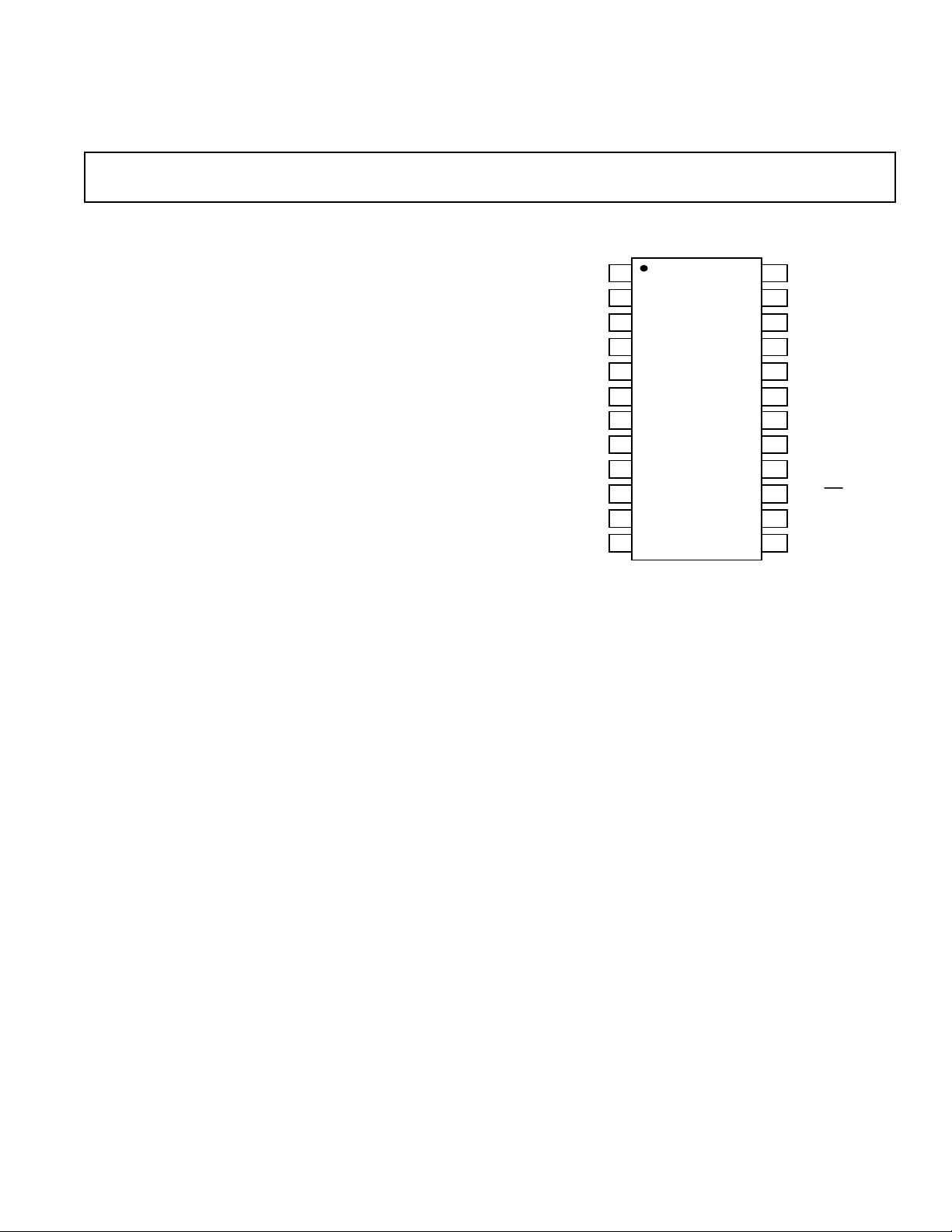
PIN FUNCTION DESCRIPTION
SOIC DIP
Pin Pin Mnemonic Function
1 19 V+ Internally Generated Positive Supply (+9 V nominal). A 0.1 µF capacitor must be connected
between this pin and GND.
2, 3 20, 22 C1+, C1– External Capacitor 1 Terminals. A 0.1 µF capacitor must be connected between these pins.
423 R2
524 T1
61 T2
72 V
83 R1
94 R1
10 5 T3
11 6 T3
IN
OUT
OUT
CC
(B) RS-422 Receiver R1, Differential Input B.
IN
/R1IN (A) Receiver R1 Input. May be configured to accept either single ended RS-232 levels or
IN
(B) RS-422 Transmitter (Driver) T3, Differential Output B.
OUT
(A) RS-232 Transmitter (Driver) T3, Differential Output A.
OUT
12, 13 16, 21 NC No Connect Pins.
14, 18 7, 11 GND Ground Pin. Must be connected to 0 V.
15 8 232/
16 9 T3
17 10 R1
19 12 T2
20 13 T1
21 14 R2
422 SEL Select Input. This input configures Receiver R1 to accept either RS-232 or RS-422 signal lev-
IN
OUT
IN
IN
OUT
22, 23 15, 17 C2+, C2– External Capacitor 2 Terminals. A 0.1 µF capacitor must be connected between these pins.
24 18 V– Internally Generated Negative Supply (–9 V nominal). A 0.1 µF capacitor must be connected
RS-232 Receiver R2 Input. This input accepts RS-232 input voltages.
RS-232 Transmitter (Driver) T1 Output (Typically ± 7.5 V).
RS-232 Transmitter (Driver) T2 Output (Typically ± 7.5 V).
Power Supply Input (5 V ± 5%).
differential RS-422 levels. It is configured using the 232/
422 SEL pin.
els. A Logic 1 on this input selects 232 operation while a Logic 0 selects 422 operation.
TTL/CMOS Input to the RS-422 Transmitter T3.
TTL/CMOS Output from Receiver R1.
TTL/CMOS Input to RS-232 Transmitter T2.
TTL/CMOS Input to RS-232 Transmitter T1.
TTL/CMOS Output from Receiver R2.
between this pin and GND.
R1
R1IN(B)
/R1IN(A)
IN
T3
T3
T1
T2
OUT
OUT
C1+
C1–
R2
OUT
OUT
V
NC
(B)
(A)
V+
IN
CC
10
11
12
SOIC
1
2
3
4
5
6
AD7306
SOIC
7
TOP VIEW
(Not to Scale)
8
9
NC = NO CONNECT
24
23
22
21
20
19
18
17
16
15
14
13
V–
C2–
C2+
R2
OUT
T1
IN
T2
IN
GND
R1
OUT
T3
IN
232/422 SEL
GND
NC
PIN CONFIGURATIONS
T2
OUT
V
R1IN(B)
R1IN/R1IN(A)
T3
(B)
OUT
T3
(A)
OUT
GND
232/422 SEL
T3
R1
OUT
GND
T2
1
2
CC
3
4
5
6
7
8
9
IN
10
11
12
IN
NC = NO CONNECT
DIP
AD7306
DIP
TOP VIEW
(Not to Scale)
24
T1
OUT
R2
23
IN
22
C1–
NC
21
20
C1+
19
V+
V–
18
17
C2–
NC
16
15
C2+
R2
14
OUT
13
T1
IN
–4–
REV. B
Page 5

AD7306
t
PLH
t
PHL
2.5V
–2.5V
0V 0V
V
OL
V
OH
R1
OUT
DIFFERENTIAL
INPUT
R1 (B) - R1 (A)
IN IN
t
EN2
t
EN1
1.5V 1.5V
V
OL
V
OH
R1
OUT
232/422 SEL
V
OL
V
OH
RS-232 RS-422
RS-232
TTL/CMOS
INPUTS
TTL/CMOS
OUTPUTS
232/422 SEL
T3
IN
+5V INPUT
0.1µF
7
V
0.1µF
0.1µF
R2
R1
2
C1+
3
C1–
22
C2+
23
C2–
20 5
T1
IN
19
T2
IN
16
T3
IN
21
OUT
17
OUT
15
POWER
SUPPLY
GENERATOR
AD7306
R1
±10V
T1
T2
T3
R2
CC
V+
V–
1418
1
24
6
10
11
4
9
8
0.1µF
0.1µF
T1
OUT
T2
OUT
T3 (B)
OUT
T3 (A)
OUT
R2
IN
R1IN/R1
R1 (B)
IN
Figure 1. AD7306 Application Circuit
T3 (B)
OUT
C = 100pF
L1
OUT
RL = 100Ω
DIFF
C = 100pF
L2
T3
T3 (A)
RS-232
OUTPUTS
RS-232
INPUT
(A)
IN
RS-422
INPUT
RS-422
OUTPUT
RS-232/
RS-422
INPUT
3V
1.5V
1.5V
0V
t
PHL
t
SKEW
90% POINT
T3 (A)
OUT
T3 (B)
OUT
VO
VO
1/2 VO
90% POINT
t
SKEW
t
PLH
0V
–VO
10% POINT
t
R
t
F
10% POINT
Figure 4. RS-422 Driver. Propagation Delay Rise/Fall
Timing
Figure 5. RS-422 Receiver Timing
Figure 2. RS-422 Driver. Propagation Delay Test Circuit
T3 (B)
OUT
OUT
V
OD
RL
DIFF
T3
IN
T3
T3 (A)
Figure 3. RS-422 Driver. Voltage Measurement Test
Circuit
REV. B
Figure 6. RS-232/RS-422 Receiver Enable Timing
–5–
Page 6

AD7306
GENERAL DESCRIPTION
The AD7306 drivers/receivers provide an interface which is
compatible with RS-232/RS-422 standard interfaces. As both
standards are widely accepted it is often necessary to provide an
interface which is compatible with both. The AD7306 is ideally
suited to this type of application as both standards may be met
using a single package. This part contains two RS-232 drivers,
one RS-422 driver, one RS-232 receiver, and one receiver path
which can be configured as either RS-232 or RS-422. This receiver is configured using the 232/
422 SEL pin.
This part also contains an internal charge pump voltage converter which facilitates operation using a single +5 V power
supply.
Charge Pump DC-DC Voltage Generator
The charge pump voltage generator uses a switched capacitor
technique to develop ±10 V levels from an input +5 V supply. A
highly efficient charge pump design coupled with a high frequency internal oscillator permit operation using four 0.1 µF
capacitors.
+10V
OUTPUT
–10V
OUTPUT
+5V
INPUT
SUPPLY
V
CC
C1+
0.1µF
±10V
POWER SUPPLY
GENERATOR
C1– C2+ C2–
C1
C2
0.1µF
V+
V–
C3
0.1µF
C4
0.1µF
Figure 7. Charge Pump Voltage Generator
Capacitors C1 and C2 act as charge storage capacitors while C3
and C4 provide output smoothing. For correct operation all four
capacitors must be included. Either polarized or nonpolarized
capacitors may be used for C1–C4. If a polarized type is used,
then the correct polarity should be observed. This may be ignored with nonpolarized type capacitors.
The charge pump output voltages, V+ and V–, are used internally to power the RS-232 transmitters. This permits RS-232
output levels to be developed on the RS-232 transmitter outputs. The charge pump output voltages may also be used to
power external circuitry if the current requirements are small.
Please refer to the Typical Performance Characteristics.
The generator rise time after power up is 200 µs typical. This
time is necessary to completely charge the storage capacitors in
the charge pump. Therefore, RS-232 data transmission should
not be initiated until this time has elapsed after switch on. This
will ensure that valid data is always transmitted.
RS-232 Drivers
The RS-232 drivers in the AD7306 meet the EIA RS-232
specifications. The drivers are inverting level shifters which
convert TTL/CMOS levels into RS-232 output levels. The input switching threshold is typically 1.3 V. With a typical
RS-232 load, the output levels are ± 7.5 V. Under worst case
load conditions, the drivers are guaranteed to provide ±5 V
which meets the minimum RS-232 requirement. The output
slew rate is internally limited to <30 V/µs without the need for
an external slew limiting capacitor. Short circuit protection is
also provided which prevents damage in the event of output
fault conditions. Active current limiting is used which limits the
output short circuit current to less than 12 mA in the event of
an output fault. This type of current limiting does not degrade
the output voltage swing under normal loading conditions as
would be the case with conventional passive limiting.
The powered-down output impedance is typically 10 MΩ. This
is considerably larger than the 300 Ω minimum value required
by the RS-232 specification. It provides additional protection
under fault conditions where another powered-up transmitter
output is inadvertently shorted to the powered-down device.
RS-232 Receivers
The receivers are inverting level shifters which accept RS-232
input levels (±3 V to ±15 V) and translates them into 5 V
TTL/CMOS levels. The input switching thresholds are 0.8 V
minimum and 2.4 V maximum which are well within the
RS-232 requirement of ±3 V. Internal 5 kΩ pull-down resistors
to GND are provided on the receiver inputs. This ensures that
an unconnected input will be interpreted as a low level giving a
Logic “1” on the TTL/CMOS output. Excellent noise immunity is achieved by the use of hysteresis and internal filtering
circuitry. The filter rejects noise glitches of up to 0.5 µs in
duration.
RS-422 Driver
The RS-422 driver on the AD7306 accepts a TTL/CMOS input and translates it into a differential RS-422 level signal. The
input switching threshold is typically 1.3 V. The unloaded output differential voltage is typically ± 5 V (see Typical Performance Characteristics). Short circuit protection is provided on
the output which limits the current to less than 150 mA.
RS-422 Receiver
The RS-422 receiver on the AD7306 accepts a differential input signal and translates it into a TTL/CMOS output level.
The input resistance on both differential inputs is 5 kΩ typical.
With the receiver inputs unconnected (floating), internal biasing ensures that the receiver output is a Logic “1.”
Excellent noise immunity and high transmission speed is
achieved using the differential configuration.
–6–
REV. B
Page 7

T ypical Performance Characteristics–AD7306
10
0
10
6
2
2
4
0
8
864
RS-232 TRANSMITTER OUTPUT CURRENT – mA
RS-232 TRANSMITTER OUTPUT VOLTAGE – ±V
–V CURRENT
E
+V CURRENT
E
6
0
60
3
1
10
2
0
5
4
50403020
DIFFERENTIAL O/P CURRENT – mA
DIFFERENTIAL O/P VOLTAGE – V
V = 5.25V
CC
V = 5.0V
CC
V = 4.75V
CC
10
90
100
0%
10ns
5
1V 1V
A3 2 4 V
10
V+
VOLTAGE OUTPUT ± – V
8
6
4
2
0
5
0
V-
V = 5V
CC
T + 25°C
OUTPUT CURRENT ± – mA
Figure 8. V+ and V– Voltage vs. Current
25
+V
20
15
10
SLEW RATE –V/µs
E
–V
E
30
25201510
Figure 11. RS-232 Driver Output Voltage vs. Current
5
0
0
LOAD CAPACITANCE – pF
200015001000500
2500
Figure 9. RS-232 Driver Slew Rate vs. Load Capacitance
A4 -0 370 V
100
90
10
0%
1µs5V 5V
Figure 10. RS-232 Driver; RL = 5 kΩ, CL = 50 pF
Figure 12. RS-422 Driver Output Current vs. Output Voltage
Figure 13. RS-422 Driver; R
= 100 Ω, CL1 = CL2 = 100 pF
LDIFF
REV. B
–7–
Page 8

AD7306
Single-Ended Data Transmission
Single-ended interfaces are used for low speed, short distance
communications such as from a computer terminal to a printer.
A single line is used to carry the signal. Various standards have
been developed to standardize the communication link, the most
popular of these being the RS-232. The RS-232 standard was
introduced in 1962 by the EIA and has been widely used
throughout the industry. The standard has been revised several
times, and the current revision is known as EIA-232E. The
RS-232 standard is suitable for single-ended data transmission
at relatively slow data rates over short distances. A typical
RS-232 interface is shown in Figure 14.
DATA
IN
TX
RS-232 CHANNEL
RX
DATA
OUT
Figure 14. Single-Ended RS-232 Interface
Table I. Comparison of RS-232 and RS-422 Interface Standards
Specification EIA-232E RS-422
Transmission Type Single-Ended Differential
Maximum Data Rate 20 kB/s 10 MB/s
Maximum Cable Length Load Dependent 4000 ft.
Minimum Driver Output Voltage ±5 V ±1.5 V
Slew Rate 30 V/µs max
Receiver Input Resistance 3 kΩ to 7 kΩ 4 kΩ min
Receiver Input Sensitivity ±3 V ±200 mV
Receiver Input Voltage Range ±15 V ±7 V
No. of Drivers per Line 1 1
No. of Receivers per Line 1 10
Differential Data Transmission
When transmitting at high data rates, over long distances and
through noisy environments, single-ended data transmission is
often inadequate. In this type of application, differential data
transmission offers superior performance. Differential transmission uses two signal lines to transmit data. It rejects ground
shifts and is insensitive to noise signals which appear as common mode voltages on the transmission lines. To accommodate
faster data communication, the differential RS-422 standard was
developed. Therefore, it can be used to reliably transmit data at
higher speeds and over longer distances than single-ended transmission. A typical RS-422 interface is shown in Figure 15.
DATA
IN
TX
RS-422 CHANNEL
RX
DATA
OUT
Figure 15. Differential RS-422 Interface
C1624a–2–8/94
0.6141 (15.60)
0.5985 (15.20)
24 13
PIN 1
0.0118 (0.30)
0.0040 (0.10)
0.0500
(1.27)
BSC
24-Lead SOIC (R-24)
0.2992 (7.60)
0.2914 (7.40)
0.4193 (10.65)
0.3937 (10.00)
0.0125 (0.32)
0.0091 (0.23)
0.0192 (0.49)
0.0138 (0.35)
121
0.1043 (2.65)
0.0926 (2.35)
SEATING
PLANE
OUTLINE DIMENSIONS
Dimensions shown in inches and (mm).
SEATING
0.0291 (0.74)
0.0098 (0.25)
0.0500 (1.27)
8°
0°
0.0157 (0.40)
x 45°
PLANE
0.016 (0.41)
NOTES
1.
2.
–8–
24-Lead Pin Plastic DIP (N-24)
1.228 (31.19)
1.226 (31.14)
0.02 (0.5)
LEAD NO. 1 IDENTIFIED BY DOT OR NOTCH.
PLASTIC LEADS WILL BE EITHER SOLDER DIPPED OR TIN LEAD PLATED
IN ACCORDANCE WITH MIL-M-385 10 REQUIREMENTS.
0.11 (2.79)
0.09 (2.28)
0.07(1.78)
0.05 (1.27)
0.260 ± 0.001
(6.61 ± 0.03)
0.130 (3.30)
0.128 (3.25)
0° - 15°
0.32 (8.128)
0.30 (7.62)
0.011 (0.28)
0.009 (0.23)
REV. B
PRINTED IN U.S.A.
 Loading...