

Page 1
LC2MOS
Quad 8-Bit D/A Converter
AD7226
FEATURES
Four 8-Bit DACs with Output Amplifiers
Skinny 20-Lead DIP, SOIC, SSOP, and PLCC Packages
Microprocessor-Compatible
TTL/CMOS-Compatible
No User Trims
Extended Temperature Range Operation
Single Supply Operation Possible
APPLICATIONS
Process Control
Automatic Test Equipment
Automatic Calibration of Large System Parameters,
e.g., Gain/Offset
GENERAL DESCRIPTION
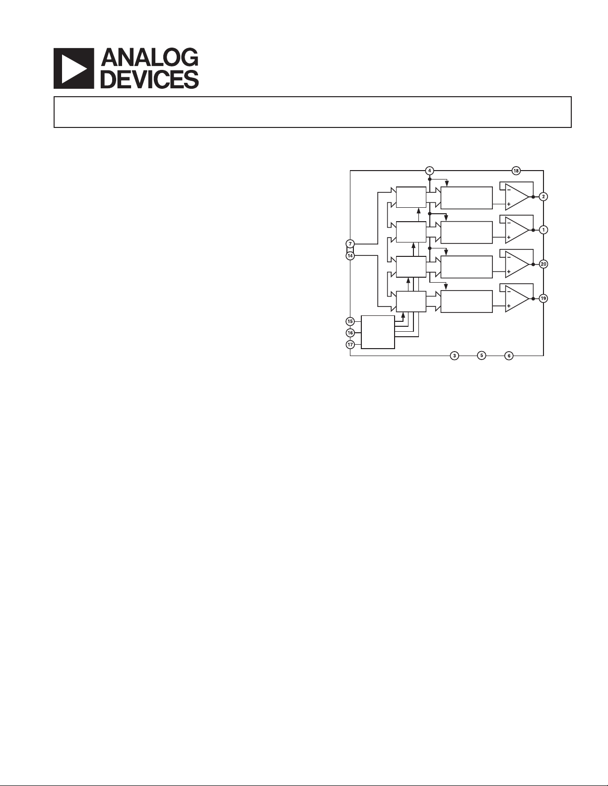
The AD7226 contains four 8-bit voltage-output digital-toanalog converters, with output buffer amplifiers and interface
logic on a single monolithic chip. No external trims are required
to achieve full specified performance for the part.
Separate on-chip latches are provided for each of the four D/A
converters. Data is transferred into one of these data latches
through a common 8-bit TTL/CMOS (5 V) compatible input
port. Control inputs A0 and A1 determine which DAC is
loaded when WR goes low. The control logic is speed-compatible with most 8-bit microprocessors.
Each D/A converter includes an output buffer amplifier capable
of driving up to 5 mA of output current. The amplifiers’ offsets
are laser-trimmed during manufacture, thereby eliminating any
requirement for offset nulling.
Specified performance is guaranteed for input reference voltages
from 2 V to 12.5 V with dual supplies. The part is also specified
for single supply operation at a reference of 10 V.
The AD7226 is fabricated in an all ion-implanted high speed
Linear Compatible CMOS (LC
2
MOS) process, which has been
specifically developed to allow high speed digital logic circuits
and precision analog circuits to be integrated on the same chip.
FUNCTIONAL BLOCK DIAGRAM
MSB
DATA
(8-BIT)
LSB
WR
V
REF
LATCH A
D
A
LATCH B
T
A
B
LATCH C
U
S
LATCH D
CONTROL
A1
A0
LOGIC
V
SS
DAC A
DAC B
DAC C
DAC D
AGND AGND
AD7226
V
DD
A
B
C
D
V
OUT
V
OUT
V
OUT
V
OUT
PRODUCT HIGHLIGHTS
1. DAC-to-DAC Matching
Since all four DACs are fabricated on the same chip at the
same time, precise matching and tracking between the DACs
is inherent.
2. Single-Supply Operation
The voltage mode configuration of the DACs allows the
AD7226 to be operated from a single power supply rail.
3. Microprocessor Compatibility
The AD7226 has a common 8-bit data bus with individual
DAC latches, providing a versatile control architecture for
simple interface to microprocessors. All latch enable signals
are level triggered.
4. Small Size
Combining four DACs and four op amps plus interface logic
into a 20-pin package allows a dramatic reduction in board
space requirements and offers increased reliability in systems
using multiple converters. Its pinout is aimed at optimizing
board layout with all the analog inputs and outputs at one
end of the package and all the digital inputs at the other.
A
B
C
D
REV. C
Information furnished by Analog Devices is believed to be accurate and
reliable. However, no responsibility is assumed by Analog Devices for its
use, nor for any infringements of patents or other rights of third parties that
may result from its use. No license is granted by implication or otherwise
under any patent or patent rights of Analog Devices. Trademarks and
registered trademarks are the property of their respective companies.
One Technology Way, P.O. Box 9106, Norwood, MA 02062-9106, U.S.A.
Tel: 781/329-4700 www.analog.com
Fax: 781/326-8703 © 2003 Analog Devices, Inc. All rights reserved.
Page 2

(VDD = 11.4 V to 16.5 V, VSS = –5 V 10%, AGND = DGND = 0 V; V
AD7226–SPECIFICATIONS
unless otherwise noted. All Specifications T
MIN
to T
unless otherwise noted.)
MAX
DUAL SUPPLY
Parameter K, B Versions
STATIC PERFORMANCE
Resolution 8 Bits
Total Unadjusted Error ± 1LSB maxV
Relative Accuracy ± 0.5 LSB max
Differential Nonlinearity ± 1LSB max Guaranteed Monotonic
Full-Scale Error ± 0.5 LSB max
Full-Scale Temperature Coefficient ± 20 ppm/∞C typ V
Zero Code Error ± 20 mV max
Zero Code Error Temperature Coefficient ± 50 mV/∞C typ
REFERENCE INPUT
Voltage Range 2 to (VDD – 4) V min to V max
Input Resistance 2 kW min
Input Capacitance
3
50 pF min Occurs when each DAC is loaded with all 0s.
200 pF max Occurs when each DAC is loaded with all 1s.
DIGITAL INPUTS
Input High Voltage, V
Input Low Voltage, V
INL
INH
2.4 V min
0.8 V max
Input Leakage Current ± 1 mA max V
Input Capacitance 8 pF max
Input Coding Binary
DYNAMIC PERFORMANCE
Voltage Output Slew Rate
Voltage Output Settling Time
4
4
2.5 V/ms min
4 ms max V
Digital Crosstalk 10 nV secs typ
Minimum Load Resistance 2 kW min V
POWER SUPPLIES
VDD Range 11.4/16.5 V min/V max For Specified Performance
I
DD
I
SS
SWITCHING CHARACTERISTICS
Address to Write Setup Time, t
Address to Write Hold Time, t
Data Valid to Write Setup Time, t
Data Valid to Write Hold Time, t
Write Pulsewidth, t
NOTES
1
Maximum possible reference voltage.
2
Temperature ranges are as follows:
3
Guaranteed by design. Not production tested.
4
Sample Tested at 25∞C to ensure compliance.
5
Switching Characteristics apply for single and dual supply operation.
Specifications subject to change without notice.
K Version: –40∞C to +85∞C
B Version: –40∞C to +85∞C
WR
AS
AH
DS
DH
13 mA max Outputs Unloaded; VIN = V
11 mA max Outputs Unloaded; VIN = V
4, 5
0ns min
0ns min
50 ns min
0ns min
50 ns min
2
Unit Conditions/Comments
= 15 V ± 5%, V
DD
= 14 V to 16.5 V, V
DD
= 0 V or V
IN
= 10 V; Settling Time to ± 1/2 LSB
REF
= 10 V
OUT
DD
= +2 V to (V
REF
= 10 V
REF
REF
– 4 V)1,
DD
= +10 V
or V
INL
or V
INL
INH
INH
REV. C–2–
Page 3

AD7226
(VDD = 15 V 5%, VSS = AGND = DGND = O V; V
SINGLE SUPPLY
All specifications T
MIN
to T
unless otherwise noted.)
MAX
Parameter K, B Versions
2
= 10 V1 unless otherwise noted.
REF
Unit Conditions/Comments
STATIC PERFORMANCE
Resolution 8 Bits
Total Unadjusted Error ± 2LSB max
Differential Nonlinearity ± 1LSB max Guaranteed Monotonic
REFERENCE INPUT
Input Resistance 2 kW min
Input Capacitance
3
50 pF min Occurs when each DAC is loaded with all 0s.
200 pF max Occurs when each DAC is loaded with all 1s.
DIGITAL INPUTS
Input High Voltage, V
Input Low Voltage, V
INH
INL
Input Leakage Current ± 1 mA max V
2.4 V min
0.8 V max
= 0 V or V
IN
DD
Input Capacitance 8 pF max
Input Coding Binary
DYNAMIC PERFORMANCE
Voltage Output Slew Rate
Voltage Output Settling Time
4
4
2V/ms min
4 ms max Settling Time to ± 1/2 LSB
Digital Crosstalk 10 nV secs typ
Minimum Load Resistance 2 kW min V
= +10 V
OUT
POWER SUPPLIES
VDD Range 14.25/15.75 V min/V max For Specified Performance
I
DD
NOTES
1
Maximum possible reference voltage.
2
Temperature ranges are as follows:
K Version: –40∞C to +85∞C
B Version: –40∞C to +85∞C
3
Guaranteed by design. Not production tested.
4
Sample Tested at 25∞C to ensure compliance.
Specifications subject to change without notice.
13 mA max Outputs Unloaded; VIN = V
ABSOLUTE MAXIMUM RATINGS
1
VDD to AGND . . . . . . . . . . . . . . . . . . . . . . . . . . –0.3 V, +17 V
to DGND . . . . . . . . . . . . . . . . . . . . . . . . . . –0.3 V, +17 V
V
DD
to AGND . . . . . . . . . . . . . . . . . . . . . . . . . . . . . –7 V, V
V
SS
VSS to DGND . . . . . . . . . . . . . . . . . . . . . . . . . . . . . –7 V, V
VDD to VSS . . . . . . . . . . . . . . . . . . . . . . . . . . . . . –0.3 V, +24 V
ORDERING GUIDE
1
Total
Temperature Unadjusted Package
Model Range Error Option
AD7226KN –40∞C to +85∞C ± 1 LSB N-20
AD7226KP –40∞C to +85∞C ± 1 LSB P-20A
AD7226KR –40∞C to +85∞C ± 1 LSB RW-20
AD7226BQ –40∞C to +85∞C ± 1 LSB Q-20
AD7226BRS –40∞C to +85∞C ± 1 LSB RS-20
NOTES
1
Dual-Supply Operation
2
N = Plastic DIP; P = Plastic Leaded Chip Carrier; Q = CERDIP; RW = SOIC;
RS = SSOP
AGND to DGND . . . . . . . . . . . . . . . . . . . . . . . . . –0.3 V, V
Digital Input Voltage to DGND . . . . . . . –0.3 V, VDD + 0.3 V
to AGND . . . . . . . . . . . . . . . . . . . . . . . . . . . –0.3 V, V
V
REF
V
2
to AGND2 . . . . . . . . . . . . . . . . . . . . . . . . . . . . VSS, V
OUT
Power Dissipation (Any Package) to 75∞C . . . . . . . . . . 500 mW
Derates above 75∞C by . . . . . . . . . . . . . . . . . . . . . 2.0 mW/∞C
Operating Temperature
Commercial (K Version) . . . . . . . . . . . . . . . –40∞C to +85∞C
Industrial (B Version) . . . . . . . . . . . . . . . . . –40∞C to +85∞C
Storage Temperature . . . . . . . . . . . . . . . . . . . –65∞C to +150∞C
Lead Temperature (Soldering, 10 secs) . . . . . . . . . . . . . 300∞C
NOTES
1
Stresses above those listed under Absolute Maximum Ratings may cause perma-
nent damage to the device. This is a stress rating only, functional operation of the
device at these or any other conditions above those indicated in the operational
sections of this specification is not implied. Exposure to absolute maximum rating
conditions for extended periods may affect device reliability.
2
Outputs may be shorted to AGND provided that the power dissipation of the
package is not exceeded. Typically short circuit current to AGND is 50 mA.
INL
or V
INH
DD
DD
DD
DD
DD
CAUTION
ESD (electrostatic discharge) sensitive device. Electrostatic charges as high as 4000 V readily
accumulate on the human body and test equipment and can discharge without detection. Although the
AD7226 features proprietary ESD protection circuitry, permanent damage may occur on devices
subjected to high energy electrostatic discharges. Therefore, proper ESD precautions are recommended
to avoid performance degradation or loss of functionality.
REV. C
–3–
Page 4
AD7226
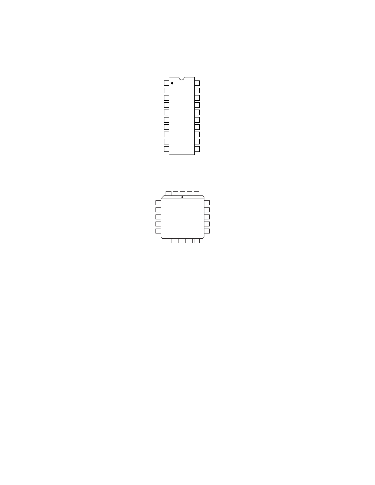
PIN CONFIGURATIONS
DIP and SOIC/SSOP
V
BV
1
OUT
V
A
2
OUT
V
3
SS
4
V
REF
5
AGND
DGND
DB7 (MSB)
DB6
DB5
DB4
AD7226
TOP VIEW
6
(Not to Scale)
7
8
9
10
PLCC
B
A
SSVOUT
OUT
V
V
3 2 1 20 19
REF
AGND
DGND
DB8
4
5
6
(Not to Scale)
7
8
9 10 11 12 13
DB5
AD7226
TOP VIEW
DB4
DB3
V
DB7 (MSB)
C
V
OUT
DB2
20
V
19
V
18
A0
17
A1
16
15
WR
14
DB0(LSB)
13
DB1
12
DB2
11
DB3
D
OUT
V
DB1
OUT
OUT
DD
18
17
16
15
14
C
D
V
DD
A0
A1
WR
DB0(LSB)
TERMINOLOGY
TOTAL UNADJUSTED ERROR
This is a comprehensive specification that includes full-scale
error, relative accuracy and zero code error. Maximum output
voltage is V
256. The LSB size will vary over the V
code error will, relative to the LSB size, increase as V
– 1 LSB (ideal), where 1 LSB (ideal) is V
REF
range. Hence the zero
REF
REF
/
REF
decreases.
Accordingly, the total unadjusted error, which includes the zero
code error, will also vary in terms of LSB’s over the V
REF
range.
As a result, total unadjusted error is specified for a fixed reference voltage of 10 V.
RELATIVE ACCURACY
Relative Accuracy or endpoint nonlinearity, is a measure of the
maximum deviation from a straight line passing through the
endpoints of the DAC transfer function. It is measured after
allowing for zero and full-scale error and is normally expressed
in LSB’s or as a percentage of full-scale reading.
DIFFERENTIAL NONLINEARITY
Differential Nonlinearity is the difference between the measured
change and the ideal 1 LSB change between any two adjacent
codes. A specified differential nonlinearity of ± 1 LSB max over
the operating temperature range ensures monotonicity.
DIGITAL CROSSTALK
The glitch impulse transferred to the output of one converter
due to a change in the digital input code to another of the converters. It is specified in nV secs and is measured at V
REF
= 0 V.
FULL SCALE ERROR
Full-Scale Error is defined as:
Measured Value – Zero Code Error – Ideal Value
REV. C–4–
Page 5
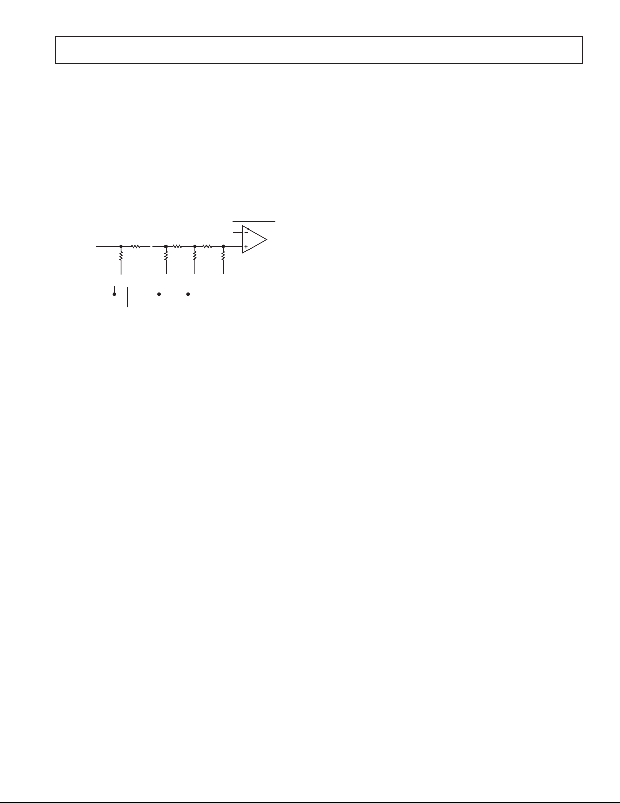
CIRCUIT INFORMATION D/A SECTION
The AD7226 contains four identical, 8-bit, voltage mode digital-toanalog converters. The output voltages from the converters have the
same polarity as the reference voltage allowing single supply operation. A novel DAC switch pair arrangement on the AD7226 allows a
reference voltage range from 2 V to 12.5 V.
Each DAC consists of a highly stable, thin-film, R-2R ladder
and eight high speed NMOS, single-pole, double-throw
switches. The simplified circuit diagram for one channel is
shown in Figure 1. Note that V
are common to all four DACs.
(Pin 4) and AGND (Pin 5)
REF
AD7226
REV. C
–5–
Page 6

AD7226
W
t
DS
t
DH
t
AH
t
AS
V
INL
V
INH
V
INH
V
INL
V
DD
V
DD
V
DD
DATA
ADDRESS
WR
0
0
0
t
WR
NOTES
1. ALL INPUT SIGNAL RISE AND FALL TIMES
MEASURED FROM 10% TO 90% OF V
DD
.
t
r
=
t
f
= 20ns OVER VDD RANGE.
2. TIMING MEASUREMENT REFERENCE LEVEL IS
3. SELECTED INPUT LATCH IS TRANSPARENT WHILE WR IS
LOW, THUS INVALID DATA DURING THIS TIME CAN CAUSE
SPURIOUS OUTPUTS.
V
INH
+ V
INL
2
INTERFACE LOGIC INFORMATION
Address lines A0 and A1 select which DAC will accept data
from the input port. Table I shows the selection table for the
four DACs with Figure 4 showing the input control logic. When
the WR signal is LOW, the input latches of the selected DAC
are transparent and its output responds to activity on the data
bus. The data is latched into the addressed DAC latch on the
rising edge of WR. While WR is high the analog outputs remain
at the value corresponding to the data held in their respective latches.
Table I. AD7226 Truth Table
AD7226 Control Inputs AD7226
WR A1 A0 Operation
HXXNo Operation Device Not Selected
LLLDAC A Transparent
LLDAC A Latched
LLHDAC B Transparent
LHDAC B Latched
LHLDAC C Transparent
HLDAC C Latched
LHHDAC D Transparent
HHDAC D Latched
L = Low State, H = High State, X = Don’t Care
A0
A1
R
TO LATCH A
TO LATCH B
TO LATCH C
TO LATCH D
Figure 4. Input Control Logic
Figure 5. Write Cycle Timing Diagram
REV. C–6–
Page 7

(TA = 25C, VDD = 15 V, VSS = –5 V)
TEMPERATURE (C)
2.0
010
ZERO CODE ERROR (LSBs)
1.5
1.0
0.5
0
–0.5
–1.0
–1.5
–2.0
20 30 40 50 60 70 80 90 100 110 120 130
V
OUT
A
V
OUT
B
V
OUT
C
V
OUT
D
Typical Performance Characteristics–AD7226
2.0
1.5
1.0
0.5
0
–0.5
–1.0
TOTA L UNADJUSTED ERROR (LSBs)
–1.5
–2.0
0
32 48 64 80 96 112 128 144 160 176 192 208 224 240 256
16
INPUT CODE (DECIMAL EQUIVALENT)
V
TPC 1. Channel-to-Channel Matching
4
3
2
1
0
REF
= 10V
AD7226K, B
4
3
2
1
0
–1
–2
DIFFERENTIAL NONLINEARITY (LSBs)
–3
–4
01424681012
V
(V)
REF
TPC 3. Differential Nonlinearity vs. V
AD7226K, B
REF
–1
–2
RELATIVE ACCURACY (LSBs)
–3
–4
01424681012
V
REF
TPC 2. Relative Accuracy vs. V
REV. C
(V)
REF
TPC 4. Zero Code Error vs. Temperature
–7–
Page 8

AD7226
SPECIFICATION RANGES
In order for the DACs to operate to their specifications, the
reference voltage must be at least 4 V below the V
supply voltage. This voltage differential is required for correct
generation of bias voltages for the DAC switches.
The AD7226 is specified to operate over a V
DD
+12 V ± 5% to +15 V ± 10% (i.e., from +11.4 V to +16.5 V)
with a V
+15 V ± 5% V
of –5 V ± 10%. Operation is also specified for a single
SS
supply. Applying a VSS of –5 V results in
DD
improved zero code error, improved output sink capability with
outputs near AGND and improved negative-going settling time.
Performance is specified over a wide range of reference voltages
from 2 V to (V
– 4 V) with dual supplies. This allows a range
DD
of standard reference generators to be used such as the AD780,
a 2.5 V band gap reference and the AD584, a precision 10 V
reference. Note that in order to achieve an output voltage range
of 0 V to 10 V a nominal 15 V ± 5% power supply voltage is
required by the AD7226.
power
DD
range from
DATA
+1/2 LSB
O/P
–1/2 LSB
Figure 7a. Positive Step Settling Time (VSS = –5 V)
DATA
SETTLING TIME
The output stage of the buffer amplifiers consists of a bipolar
NPN transistor from the V
. VSS is the negative power supply for the output buffer ampli-
V
SS
line and a constant current load to
DD
fiers. As mentioned in the op amp section, in single supply
operation the NMOS transistor will come out of saturation as the
output voltage approaches AGND and will act as a resistive load
of approximately 2 kW to AGND. As a result, the settling time for
negative-going signals approaching AGND in single supply operation will be longer than for dual supply operation where the
current load of 400 mA is maintained all the way down to AGND.
Positive-going settling-time is not affected by V
.
SS
The settling-time for the AD7226 is limited by the slew-rate of
the output buffer amplifiers. This can be seen from Figure 6
which shows the dynamic response for the AD7226 for a full
scale change. Figures 7a and 7b show expanded settling-time
photographs with the output waveforms derived from a differential input to an oscilloscope. Figure 7a shows the settling time
for a positive-going step and Figure 7b shows the settling time
for a negative-going output step.
DATA
V
OUT
+1/2 LSB
O/P
–1/2 LSB
Figure 7b. Negative Step Settling Time (VSS = –5 V)
GROUND MANAGEMENT
AC or transient voltages between AGND and DGND can cause
noise at the analog output. This is especially true in microprocessor systems where digital noise is prevalent. The simplest
method of ensuring that voltages at AGND and DGND are
equal is to tie AGND and DGND together at the AD7226. In
more complex systems where the AGND and DGND intertie is
on the backplane, it is recommended that two diodes be connected in inverse parallel between the AD7226 AGND and
DGND pins (IN914 or equivalent).
Unipolar Output Operation
This is the basic mode of operation for each channel of the
AD7226, with the output voltage having the same positive
polarity as +V
(V
= AGND) or with positive/negative supplies (see op amp
SS
section which outlines the advantages of having negative V
. The AD7226 can be operated single supply
REF
).
SS
The code table for unipolar output operation is shown in Table
II. Note that the voltage at V
must never be negative with
REF
respect to DGND in order to prevent parasitic transistor turn-on.
Connections for the unipolar output operation are shown in
Figure 8.
Figure 6. Dynamic Response (VSS = –5 V)
REV. C–8–
Page 9

AD7226
DAC A
V
REF
V
DD
DGND
AGND
V
SS
V
OUT
A
V
OUT
V
REF
AD7226
*
R2
R1
+15V
–15V
R1, R2 = 10k 0.1%
*
DIGITAL INPUTS OMITTED
FOR CLARITY
VAV DV
OUT BIAS A IN
=+
()
AGND
V
DD
DGND
MSB
LSB
WR
A1
A0
DB7
DB0
V
REF
DAC A
DAC B
DAC C
DAC D
V
SS
Figure 8. AD7226 Unipolar Output Circuit
Table II. Unipolar Code Table
DAC Latch Contents
MSB LSB Analog Output
With R1 = R2
VDV
=
()
OUT A REF
V
OUT
A
where DA is a fractional representation of the digital word in latch A.
¥21–
(4)
Mismatch between R1 and R2 causes gain and offset errors and
V
B
OUT
therefore these resistors must match and track over temperature. Once again the AD7226 can be operated in single supply
or from positive/negative supplies. Table III shows the digital
code versus output voltage relationship for the circuit of Figure 9
V
C
OUT
V
D
OUT
with R1 = R2.
Figure 9. AD7226 Bipolar Output Circuit
Table III. Bipolar (Offset Binary) Code Table
1 1 1 1 1 1 1 1
1 0 0 0 0 0 0 1
1 0 0 0 0 0 0 0
0 1 1 1 1 1 1 1
0 0 0 0 0 0 0 1
0 0 0 0 0 0 0 0 0 V
Note LSB V V
:
Bipolar Output Operation
Each of the DACs of the AD7226 can be individually configured to provide bipolar output operation. This is possible using
one external amplifier and two resistors per channel. Figure 9
shows a circuit used to implement offset binary coding (bipolar
operation) with DAC A of the AD7226. In this case
V
REV. C
=+
OUT A REF REF
=
()
REF REF
Ê
Á
Ë
ˆ
R
2
1
R
˜
1
¯
¥
Ê
ˆ
+
+
+
+
+
–
8
=
2
()
–
Ê
Á
Ë
DV
()
255
V
Á
REF
Ë
256
Ê
129
V
Á
REF
Ë
256
Ê
128
Á
REF
Ë
256 2
Ê
127
V
Á
REF
Ë
256
Ê
V
Ê
Á
Ë
R
R
1
Á
REF
Ë
256
ˆ
1
˜
256
¯
ˆ
2
V
¥
()
˜
1
¯
˜
¯
ˆ
˜
¯
ˆ
˜
¯
ˆ
˜
¯
ˆ
˜
¯
DAC Latch Contents
MSB LSB Analog Output
Ê
ˆ
1 1 1 1 1 1 1 1
V
REF
=+V
1 0 0 0 0 0 0 1
+
+
127
V
Á
Ë
Ê
Á
Ë
128
1
128
˜
¯
ˆ
˜
¯
REF
V
REF
1 0 0 0 0 0 0 0 0 V
Ê
ˆ
1
Á
Ë
Ê
Á
Ë
Ê
Á
Ë
128
127
128
128
128
˜
¯
ˆ
˜
¯
ˆ
=
˜
¯
REF
REF
REF REF
(2)
0 1 1 1 1 1 1 1
0 0 0 0 0 0 0 1
0 0 0 0 0 0 0 0
AGND BIAS
–V
–V
––VV
The AD7226 AGND pin can be biased above system GND
(AD7226 DGND) to provide an offset “zero” analog output
voltage level. Figure 10 shows a circuit configuration to achieve
this for channel A of the AD7226. The output voltage, V
OUT
A,
can be expressed as:
(5)
where DA is a fractional representation of the digital input word
(0 £ D £ 255/256).
(3)
–9–
Page 10

AD7226
REV. C–10–
Page 11

AD7226
STAIRCASE WINDOW COMPARATOR
In many test systems, it is important to be able to determine
whether some parameter lies within defined limits. The staircase
window comparator of Figure 14a is a circuit that can be used,
for example, to measure the V
device under test. Upper and lower limits on both V
and VOL thresholds of a TTL
OH
OH
and V
OL
can be programmably set using the AD7226. Each adjacent pair
of comparators forms a window of programmable size. If V
TEST
lies within a window, then the output for that window will be
high. With a reference of 2.56 V applied to the V
input, the
REF
minimum window size is 10 mV.
V
TEST
V
REF
V
OUT
V
OUT
AD7226
V
OUT
V
OUT
AGND
FROM D.U.T.
V
DD
(HIGH)
V
OH
A
(LOW)
V
OH
B
V
(HIGH)
OL
C
V
(LOW)
OL
D
1/4 CA339
5V
5V
5V
5V
5V
10k
10k
10k
10k
10k
WINDOW 1
WINDOW 2
WINDOW 3
WINDOW 4
WINDOW 5
Figure 14a. Logic Level Measurement
V
REF
V
OUT
V
OUT
AD7226
V
OUT
V
OUT
AGND
Figure 15a. Overlapping Windows
+4V
–4V
*
DIGITAL INPUTS OMITTED
FOR CLARITY
+15V
V
TEST
FROM D.U.T.
10k
V
A
B
C
D
V
V
OUT
V
OUT
V
OUT
V
OUT
AGND
REF
DD
B
A
D
C
WINDOW 2
5V
10k
5V
10k
5V
WINDOW 1
WINDOW 3
Figure 15b. Window Structure
15k
10k
V
REF
*
AD7226
DAC A
WINDOW 1
WINDOW 2
WINDOW 3
V
DD
V
A
OUT
V
REF
WINDOW 1
V
A
OUT
V
OUT
V
OUT
V
OUT
AGND
WINDOW 2
B
WINDOW 3
C
WINDOW 4
D
WINDOW 5
Figure 14b. Window Structure
The circuit can easily be adapted to allow for overlapping of
windows as shown in Figure 15a. If the three outputs from this
circuit are decoded then five different nonoverlapping programmable windows can again be defined.
REV. C
–11–
V
AGND
SS
DGND
Figure 16. Varying Reference Signal
VARYING REFERENCE SIGNAL
In some applications, it may be desirable to have a varying signal
applied to the reference input of the AD7226. The AD7226 has
multiplying capability within upper and lower limits of reference
voltage when operated with dual supplies. The upper and lower
limits are those required by the AD7226 to achieve its linearity
specification. Figure 16 shows a sine wave signal applied to the
reference input of the AD7226. For input signal frequencies up
to 50 kHz, the output distortion typically remains less than 0.1%.
Typical 3 dB bandwidth figure is 700 kHz.
Page 12

AD7226
OFFSET ADJUST
Figure 17 shows how the AD7226 can be used to provide programmable input offset voltage adjustment for the AD544 op
amp. Each output of the AD7226 can be used to trim the input
offset voltage on one AD544. The 620 kW resistor tied to 10 V
provides a fixed bias current to one offset node. For symmetrical adjustment, this bias current should equal the current in the
other offset node with the half-full scale code (i.e., 10000000)
on the DAC. Changing the code on the DAC varies the bias
current and hence provides offset adjust for the AD544. For
example, the input offset voltage on the AD544J, which has a
maximum of ± 2 mV, can be programmably trimmed to ± 10 mV.
8085A
A15
A8
WR
ALE
D7
D0
8212DS2
*
LINEAR CIRCUITRY OMITTED FOR CLARITY
ADDRESS BUS
ADDRESS
EN
DECODE
ADDRESS/DATA BUS
AD7226
WR
A0
A1
DB7
DB0
*
Figure 18. AD7226 to 8085A Interface
+10V
V
REF
AD7226
DAC A
V
*
AGND
SS
V
DD
V
A
OUT
DGND
*
DIGITAL INPUTS OMITTED
FOR CLARITY
Figure 17. Offset Adjust for AD544
A15
6502
A0
R/W
2
D7
D0
ADDRESS BUS
ADDRESS
EN
DECODE
EN
DATA BUS
*
LINEAR CIRCUITRY OMITTED FOR CLARITY
Figure 20. AD7226 to 6502 Interface
500k
+15V
1
–15V
7
5
4
A0
A1
WR
AD7226
DB7
DB0
620k
*
A15
6809
A0
R/W
D7
D0
ADDRESS BUS
ADDRESS
EN
DECODE
EN
E
DATA BUS
*
LINEAR CIRCUITRY OMITTED FOR CLARITY
Figure 19. AD7226 to 6809 Interface
A0
A1
WR
AD7226
DB7
DB0
A15
Z-80
A0
WR
*
D7
D0
ADDRESS BUS
ADDRESS
EN
DECODE
DATA BUS
*
LINEAR CIRCUITRY OMITTED FOR CLARITY
A0
A1
WR
AD7226
DB7
DB0
*
Figure 21. AD7226 to Z-80 Interface
REV. C–12–
Page 13

20-Lead Plastic Dual In-Line Package [PDIP]
(N-20)
Dimensions shown in inches and (millimeters)
0.985 (25.02)
0.965 (24.51)
0.945 (24.00)
20
1
0.180 (4.57)
MAX
0.150 (3.81)
0.130 (3.30)
0.110 (2.79)
0.022 (0.56)
0.018 (0.46)
0.014 (0.36)
CONTROLLING DIMENSIONS ARE IN INCHES; MILLIMETER DIMENSIONS
(IN PARENTHESES) ARE ROUNDED-OFF INCH EQUIVALENTS FOR
REFERENCE ONLY AND ARE NOT APPROPRIATE FOR USE IN DESIGN
COMPLIANT TO JEDEC STANDARDS MO-095-AE
0.015 (0.38) MIN
0.100
0.060 (1.52)
(2.54)
0.050 (1.27)
BSC
0.045 (1.14)
0.295 (7.49)
0.285 (7.24)
0.275 (6.99)
11
10
SEATING
PLANE
0.325 (8.26)
0.310 (7.87)
0.300 (7.62)
0.015 (0.38)
0.010 (0.25)
0.008 (0.20)
20-Lead Ceramic Dual In-Line Package [CERDIP]
(Q-20)Q-2OTc 0.0173E(0.060 Dimensions shown in inches and4)millimetersET/GS113 EmbeddedDocument /MC1 BDC 0 k190.5 gsBT/T12 l9 9 35627.8821.64-547 37 0 0 1.62.8 565 M90.j90..107 l9 9 35627.8821.64-547 37 0 44 2 T1.0235627.8821.64-547 37 0 0 2 T1.0235627.8821.64-547 37 0 44 6578.8235627.8821.64-547 37 0 0 6578.8235627.8821.64-547 37 0 44 6929235627.8821.64-547 37 0 0 6929235627.8821.64-547 37 0 44 7 Td1235627.8821.64-547 37 0 0 7 Td1235627.8821.64-547 37 0 44 l997.35627.8821.64-547 37 0 0 l997.35627.8821.64-547 37 0 44 5)Tj9235627.8821.64-547 37 0 0 5
0.150 (3.81)
0.135 (3.43)
0.120 (3.05)
AD7226
REV. C
–13–
Page 14

AD7226
OUTLINE DIMENSIONS
20-Lead Standard Small Outline Package [SOIC]
Wide Body
(RW-20)
Dimensions shown in millimeters and (inches)
13.00 (0.5118)
12.60 (0.4961)
0.30 (0.0118)
0.10 (0.0039)
0.048 (1.21)
0.042 (1.07)
20 11
1
1.27
COPLANARITY
0.10
CONTROLLING DIMENSIONS ARE IN MILLIMETERS; INCH DIMENSIONS
(IN PARENTHESES) ARE ROUNDED-OFF MILLIMETER EQUIVALENTS FOR
REFERENCE ONLY AND ARE NOT APPROPRIATE FOR USE IN DESIGN
COMPLIANT TO JEDEC STANDARDS MS-013AC
(0.0500)
BSC
0.51 (0.0201)
0.33 (0.0130)
7.60 (0.2992)
7.40 (0.2913)
10
2.65 (0.1043)
2.35 (0.0925)
SEATING
PLANE
10.65 (0.4193)
10.00 (0.3937)
0.32 (0.0126)
0.23 (0.0091)
20-Lead Plastic Leaded Chip Carrier [PLCC]
(P-20A)
Dimensions shown in inches and (millimeters)
0.048 (1.21)
0.042 (1.07)
3
4
TOP VIEW
(PINS DOWN)
8
0.020
(0.50)
9
0.356 (9.04)
R
0.350 (8.89)
0.395 (10.02)
0.385 (9.78)
CONTROLLING DIMENSIONS ARE IN INCHES; MILLIMETER DIMENSIONS
(IN PARENTHESES) ARE ROUNDED-OFF INCH EQUIVALENTS FOR
REFERENCE ONLY AND ARE NOT APPROPRIATE FOR USE IN DESIGN
0.056 (1.42)
0.042 (1.07)
19
18
0.050
(1.27)
BSC
14
13
SQ
SQ
COMPLIANT TO JEDEC STANDARDS MO-047AA
0.180 (4.57)
0.165 (4.19)
0.120 (3.04)
0.090 (2.29)
0.20 (0.51)
MIN
0.021 (0.53)
0.013 (0.33)
0.032 (0.81)
0.026 (0.66)
0.040 (1.01)
0.025 (0.64)
0.75 (0.0295)
0.25 (0.0098)
8ⴗ
0ⴗ
0.020 (0.50)
0.330 (8.38)
0.290 (7.37)
1.27 (0.0500)
0.40 (0.0157)
R
ⴛ 45ⴗ
BOTTOM
VIEW
(PINS UP)
REV. C–14–
Page 15

AD7226
Revision History
Location Page
3/03—Data Sheet changed from REV. B to REV. C.
Title Revision . . . . . . . . . . . . . . . . . . . . . . . . . . . . . . . . . . . . . . . . . . . . . . . . . . . . . . . . . . . . . . . . . . . . . . . . . . . . . . . . . . . . . . . . . . 1
3/03—Data Sheet changed from REV. A to REV. B.
Edits to FEATURES . . . . . . . . . . . . . . . . . . . . . . . . . . . . . . . . . . . . . . . . . . . . . . . . . . . . . . . . . . . . . . . . . . . . . . . . . . . . . . . . . . . . . 1
Edits to SPECIFICATIONS . . . . . . . . . . . . . . . . . . . . . . . . . . . . . . . . . . . . . . . . . . . . . . . . . . . . . . . . . . . . . . . . . . . . . . . . . . . . . . . 2
Edits to ORDERING GUIDE . . . . . . . . . . . . . . . . . . . . . . . . . . . . . . . . . . . . . . . . . . . . . . . . . . . . . . . . . . . . . . . . . . . . . . . . . . . . . . 3
Edits to ABSOLUTE MAXIMUM RATINGS . . . . . . . . . . . . . . . . . . . . . . . . . . . . . . . . . . . . . . . . . . . . . . . . . . . . . . . . . . . . . . . . . 3
Edits to PIN CONFIGURATIONS . . . . . . . . . . . . . . . . . . . . . . . . . . . . . . . . . . . . . . . . . . . . . . . . . . . . . . . . . . . . . . . . . . . . . . . . . 4
Edits to SPECIFICATIONS RANGES . . . . . . . . . . . . . . . . . . . . . . . . . . . . . . . . . . . . . . . . . . . . . . . . . . . . . . . . . . . . . . . . . . . . . . 8
OUTLINE DIMENSIONS updated . . . . . . . . . . . . . . . . . . . . . . . . . . . . . . . . . . . . . . . . . . . . . . . . . . . . . . . . . . . . . . . . . . . . . . . . 13
RS-20 package added . . . . . . . . . . . . . . . . . . . . . . . . . . . . . . . . . . . . . . . . . . . . . . . . . . . . . . . . . . . . . . . . . . . . . . . . . . . . . . . . . . . 13
Updated RS-20 package OUTLINE DIMENSIONS . . . . . . . . . . . . . . . . . . . . . . . . . . . . . . . . . . . . . . . . . . . . . . . . . . . . . . . . . . . 13
REV. C
–15–
Page 16

C00987–0–3/03(C)
–16–
 Loading...