

Page 1
a
SYNC
DECODER
BURST
C-SYNC
4FSC
ENCD
RED
GREEN
BLUE
QUADRATURE
DECODER
DELAYED C-SYNC
SC 90
°
SC 0
°
CLOCK
AT 8FSC
DC
RESTORE
AND C-SYNC
INSERTION
5MHz
2-POLE
LP POST-
FILTER
COMPOSITE OUTPUT*
–0.572V TO 2V NTSC
–0.6V TO 2V PAL
LUMINANCE OUTPUT*
–0.572V TO 1.43V NTSC
–0.6V TO 1.4V PAL
CHROMINANCE OUTPUT*
572mVp-p NTSC
600mVp-p PAL
NTSC/PAL
C-SYNC
DELAY
±180
°
(PAL ONLY)
RGB-TO-YUV
ENCODING
MATRIX
BURST
Y
U
V
SC 90
°
/270
°
5MHz
4-POLE LP
PRE-FILTER
1.2MHz
4-POLE
LPF
1.2MHz
4-POLE
LPF
SAMPLED-
DATA
DELAY LINE
∑
3.6MHz (NTSC)
4.4MHz (PAL)
3-POLE LPF
∑
X2
X2
X2
POWER AND GROUNDS
+5V
AGND
DGND
LOGIC
ANALOG
ANALOG ONLY
ANALOG
LOGIC
+5V
–5V
*NOTE:
THE LUMINANCE, COMPOSITE, AND CHROMINANCE
OUTPUTS ARE AT TWICE NORMAL LEVELS FOR
DRIVING 75Ω REVERSE-TERMINATED LINES.
ASNC
NTSC/PAL
BALANCED
MODULATORS
NTSC/
PAL
X2
X2
X2
ROUT
1.5Vp-p
GOUT
1.5Vp-p
BOUT
1.5Vp-p
AD721
(ONLY)
NTSC/PAL
RGB to NTSC/PAL Encoders
AD720/AD721
FEATURES
Composite Video Output
Chrominance and Luminance (S-Video) Outputs
No External Filters or Delay Lines Required
Drives 75 Ω Reverse-Terminated Loads
Compact 28-Pin PLCC
Logic Selectable NTSC or PAL Encoding Modes
Automatically Selects Proper Chrominance Filter
Cutoff Frequency for Encoding Standard
Logic Selectable Encode or Power-Down Mode (AD720
Only)
Logic Selectable Encode or Bypass Mode (AD721 Only)
Low Power: 200 mW typical
APPLICATIONS
RGB to NTSC or PAL Encoding
Drive RGB Signals into 75 Ω Load (AD721 Only)
PRODUCT DESCRIPTION
The AD720 and AD721 RGB to NTSC/PAL Encoders convert
red, green and blue color component signals into their corresponding luminance (baseband amplitude) and chrominance
FUNCTIONAL BLOCK DIAGRAM
(subcarrier amplitude and phase) signals in accordance with
either NTSC or PAL standards. These two outputs are also
combined to provide a composite video output. All three outputs are available separately at voltages of twice the standard
signal levels as required for driving 75 Ω reverse terminated
cables. The AD721 also features a bypass mode, in which the
RGB inputs may bypass the encoder section of the IC via three
gain-of-two amplifiers suitable for driving 75Ω reverse terminated cables.
The AD720 and AD721 provide a complete, fully calibrated
function, requiring only termination resistors, bypass capacitors,
a clock input at four times the subcarrier frequency, and a composite sync pulse. There are two control inputs: one input
selects the TV standard (NTSC/PAL) and the other (ENCD)
powers down most sections of the chip when the encoding function is not in use (AD720) or activates the triple bypass buffer to
drive the RGB signals when RGB encoding is not required
(AD721). All logical inputs are CMOS compatible. The chip
operates from ± 5 V supplies.
(continued on page 5)
REV. 0
Information furnished by Analog Devices is believed to be accurate and
reliable. However, no responsibility is assumed by Analog Devices for its
use, nor for any infringements of patents or other rights of third parties
which may result from its use. No license is granted by implication or
otherwise under any patent or patent rights of Analog Devices.
One Technology Way, P.O. Box 9106, Norwood. MA 02062-9106, U.S.A.
Tel: 617/329-4700 Fax: 617/326-8703
Page 2

AD720/AD721–SPECIFICATIONS
(TA = +25°C and supplies = ±5 V unless otherwise noted)
Parameter Conditions Min Typ Max Unit
SIGNAL INPUTS (RDIN, GRIN, BLIN)
Input Amplitude NTSC 714 mV
PAL 700 mV
Input Resistances
1
RDIN with Respect to AGND 2.3 kΩ
GRIN with Respect to AGND 4.2 kΩ
BLIN with Respect to AGND 4.2 kΩ
Input Capacitance 5pF
LOGIC INPUTS (C-SYNC, 4FSC, ENCD, NTSC)
Logic LO Input Voltage 1 V
Logic HI Input Voltage 4 V
Logic LO Input Current (DC) <1 µA
Logic HI Input Current (DC) <1 µA
BYPASS AMPLIFIERS (AD721 Only)
Gain Error Nominal Gain of ×2
2
–5 +5 %
Small Signal –3 dB Bandwidth 100 MHz
Output Offset Voltage (Active State) –50 +50 mV
Output Voltage (Inactive State) –50 +50 mV
VIDEO OUTPUTS3 (LUMA, CRMA, CMPS)
Luminance (LUMA) Output
Bandwidth 5 MHz
Gain Error –5 ±1 +5 %
Linearity ±0.1 %
Sync Level NTSC 252 286 320 mV
PAL 300 mV
Chrominance (CRMA) Output
Bandwidth NTSC 3.6 MHz
PAL 4.4 MHz
Color Burst Amplitude NTSC 257 286 315 mV p-p
PAL 300 mV p-p
Absolute Gain Error –15 ±5 +15 %
Absolute Phase Error ±3 Degrees
Chroma/Luma Time Alignment
4
NTSC –170 ns
Composite Output
Absolute Gain Error –5 ±1 +5 %
Differential Gain With Respect to Chroma Channel 0.1 %
Differential Phase With Respect to Chroma Channel 0.1 Degrees
Output Offset Voltage Chroma, Luma, or Composite Outputs 50 100 mV
Chroma Feedthrough Monochrome Input 20 55 mV p-p
POWER SUPPLIES (APOS, DPOS, VNEG)
Recommended Supply Range Dual Supply ±4.75 ±5.25 V
Full Output Current
5
–5 V Supply 35 mA
+5 V Supply 67 mA
Zero Signal Quiescent Current –5 V Supply 10 20 35 mA
+5 V Supply 10 20 35 mA
Bypass Mode Quiescent Current –5 V Supply 14 20 mA
(AD721 Only) +5 V Supply 14 20 mA
NOTES
1
Input scaling resistors provide best scaling accuracy when source resistance is 37.5 Ω (75 Ω reverse-terminated input).
2
Required for driving a 75 Ω double reverse terminated load.
3
All outputs are measured at a reverse-terminated load; voltages at IC pins are twice those specified here.
4
This is a predistortion (per FCC specifications) that compensates for the chroma/luma delay in the low-pass filter that separates the luminance and chrominance
signals in a television receiver.
5
CRMA, LUMA, and CMPS outputs are all connected to 75 Ω reverse-terminated loads; full-white signal for entire field.
Specifications shown in boldface are tested on all production units at final electrical test. Results from those tests are used to calculate outgoing quality levels. All min
and max specifications are guaranteed, although only those shown in boldface are tested on all production units.
Specifications subject to change without notice.
–2–
REV. 0
Page 3
AD720/AD721
WARNING!
ESD SENSITIVE DEVICE
ABSOLUTE MAXIMUM RATINGS*
PIN DESCRIPTIONS
Supply Voltage ±VS . . . . . . . . . . . . . . . . . . . . . . . . . . . . .±6V
Internal Power Dissipation . . . . . . . . . . . . . . . . . . . . . .600 mW
Operating Temperature Range . . . . . . . . . . . . . . 0°C to +70°C
Storage Temperature Range . . . . . . . . . . . . –65°C to +150°C
Lead Temperature, Soldering 60sec . . . . . . . . . . . . . . +300°C
NOTE
*Stresses above those listed under “Absolute Maximum Ratings” may cause
permanent damage to the device. This is a stress rating only, and functional
operation of the device at these or any other conditions above those indicated in the
operational section of this specification is not implied. Exposure to absolute
maximum rating conditions for extended rating conditions for extended periods
may affect device reliability.
Thermal characteristics: 28-pin plastic package: θJA = 100°C.
ORDERING GUIDE
Temperature Package
Model Range Package Option
AD720JP 0°C to +70°C 28-Pin PLCC P-28A
AD721JP 0°C to +70°C 28-Pin PLCC P-28A
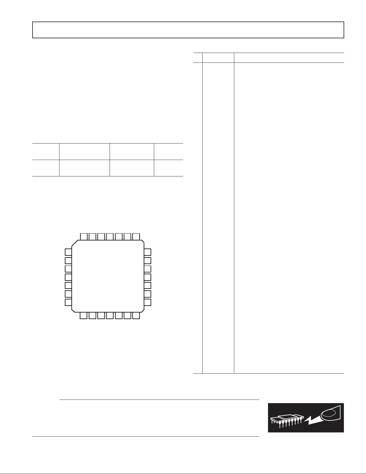
PIN CONNECTIONS
28-Lead Plastic Leaded Chip Carrier (PLCC) Package
P-28A
APOS
APOS
VNEG
BOUT (NC)
261
VNEG
LUMA
25
DGND
24
SYNC
23
DPOS
22
ASNC
21
DPOS
4FSC
20
19
DGND
AGND
5
ENCD
RDIN
6
7
AGND
GRIN
8
AGND
9
10
BLIN
STND
11
NOTE:
CONNECTIONS IN ( ) PERTAIN ONLY TO AD720
RGB TO NTSC/PAL
12
13 14 15 16 17 18
AGND
GOUT (NC)
APOS (NC)
ROUT (NC)
234
AD720/AD721
ENCODER
APOS
CMPS
CRMA
28 27
Pin Mnemonic* Description*
1 (NC) GOUT (No Connection) Green Bypass Buffer
2 (NC) APOS (No Connection) Analog Positive Supply; +5V ± 5%
3 (NC) ROUT (No Connection) Red Bypass Buffer
4 AGND Analog Ground Connection
5 ENCD A Logical High Enables the NTSC/PAL Encode
Mode (A Logical Low Powers Down the Chip)
A Logical Low Enables the RGB Bypass Mode
6 RDIN Red Component Video Input
0 mV to 714 mV for NTSC
0 mV to 700 mV for PAL
7 AGND Analog Ground Connection
8 GRIN Green Component Video Input
0 mV to 714 mV for NTSC
0 mV to 700 mV for PAL
9 AGND Analog Ground Connection
10 BLIN Blue Component Video Input
0 mV to 714 mV for NTSC
0 mV to 700 mV for PAL
11 STND A Logical High Input Selects NTSC Encoding
A Logical Low Input Selects PAL Encoding
CMOS Logic Levels
12 AGND Analog Ground Connection
13 CRMA Chrominance Output; Subcarrier Only**
572 mV Peak-to-Peak for NTSC
600 mV Peak-to-Peak for PAL
14 APOS Analog Positive Supply; +5 V ± 5%
15 CMPS Composite Video Output**
–572 mV to 2 V for NTSC
–600 mV to 2 V for PAL
16 APOS Analog Positive Supply; +5 V ± 5%
17 LUMA Luminance Plus SYNC Output**
–572 mV to 1.43 V for NTSC
–600 mV to 1.4 V for PAL
18 VNEG System Negative Supply; –5V ± 5%
19 DGND Digital Ground Connection
20 4FSC Clock Input at Four Times the Subcarrier Frequency
14.318 180 MHz for NTSC
17.734 480 MHz for PAL
CMOS Logic Levels
21 DPOS Digital Positive Supply; +5V ± 5%
22 ASNC A Logical High Input Resets the Subcarrier Phase
Every Frame
A Logical Low Input Resets the Subcarrier Phase
Every Fourth Frame
CMOS Logic Levels
23 DPOS Digital Positive Supply; +5V ± 5%
24 SYNC Input for Composite Television
Synchronization Pulses
Negative Sync Pulses
CMOS Logic Levels
25 DGND Digital Ground Connections (One of Two)
26 VNEG System Negative Supply; –5V ± 5%
27 (NC) BOUT (No Connection) Blue Bypass Buffer
28 APOS Analog Positive Supply; +5 V ± 5%
*( ) pertain only to AD720.
**The luminance, chrominance, and composite outputs are at twice normal
levels for driving 75 Ω reverse-terminated lines.
CAUTION
ESD (electrostatic discharge) sensitive device. Electrostatic charges as high as 4000 V readily
accumulate on the human body and test equipment and can discharge without detection.
Although the AD720/AD721 features proprietary ESD protection circuitry, permanent damage
may occur on devices subjected to high energy electrostatic discharges. Therefore, proper ESD
precautions are recommended to avoid performance degradation or loss of functionality.
REV. 0
–3–
Page 4

AD720/AD721–Typical Characteristics
COMPOSITE VIDEO
COMPOSITE
TEKTRONIX TSG 300
COMPONENT VIDEO
WAVEFORM GENERATOR
GENLOCK
RGB
SYNC
3
75Ω
AD720/AD721
RGB TO NTSC/PAL
ENCODER
SONY
MONITOR
MODEL 1342
75Ω
4FSC
TEKTRONIX 1910
COMPOSITE VIDEO
WAVEFORM GENERATOR
FSC
PIXEL-CLOCK
GENERATOR
TEKTRONIX VM700A
WAVEFORM MONITOR
Figure 1. AD720/AD721 Evaluation Setup
DG DP(NTSC) (SYNC = EXT)
FIELD = 1 LINE = 21
DIFFERENTIAL GAIN (%) MIN = –0.10; MAX = 0.00; p-p/MAX = 0.10
0.00 –0.04 0.00 –0.01
0.10
–0.04 –0.10
0.05
0.00
–0.05
–0.10
DIFFERENTIAL PHASE (°) MIN = 0.00; MAX = 0.07; p-p = 0.07
0.00 0.05 0.05 0.04
0.10
0.07 0.01
0.05
0.00
–0.05
–0.10
1ST
2ND 3RD 4TH
5TH 6TH
Figure 2. Composite Output Differential Phase and Gain,
NTSC (Nulled to Chroma Output)
VOLTS
0.5
0.0 70.060.050.040.030.020.010.0
0.0
IRE:FLT
100.0
50.0
0.0
FRAMES SELECTED: 1 2; APL = 45.8%
525 LINE NTSC; NO FILTERING
SLOW CLAMP TO 0.00V AT 6.63µs
MICROSECONDS
Figure 4. 100% Color Bars, NTSC
VOLTS
IRE:FLT
100.0
0.5
50.0
0.0
FRAMES SELECTED: 1 2; APL = 11.3%
525 LINE NTSC; NO FILTERING
SLOW CLAMP TO 0.00V AT 6.63µs
PRECISION MODE OFF
SYNC = SOURCE
70.060.050.040.030.020.010.0
PRECISION MODE OFF
SYNC = SOURCE
VOLTS
IRE:FLT
100.0
0.5
50.0
0.0
0.0
MICROSECONDS/PRECISION MODE OFF
NOISE REDUCTION: 15.05dB
APL = 49.6%
525 LINE NTSC; NO FILTERING
SLOW CLAMP TO 0.00V AT 6.63µs
SYNC = SOURCE
FRAMES SELECTED: 1 2
70.060.050.040.030.020.010.0
Figure 3. Modulated Pulse and Bar, NTSC
H TIMING (PAL)
LINE = 17
81ns
4.82µs
5.52µs
82ns
302.2mV
0.0 70.060.050.040.030.020.010.0
0.0
MICROSECONDS
Figure 5. Multipulse, NTSC
H TIMING MEASUREMENT RS-170A (NTSC)
FIELD = 1 LINE = 22
5.35µs
8.0
CYCLES
4.82µs
85ns
73ns
39.4 IRE
AVERAGE 32 TO 32
Figure 6. Horizontal Timing, NTSC
1.98µs
292.1mV
70.060.050.040.030.020.010.0
39.2 IRE
AVERAGE 32 TO 32
Figure 7. Horizontal Timing, PAL
–4–
REV. 0
Page 5

AD720/AD721
SYNC
DECODER
BURST
C-SYNC
4FSC
ENCD
RED
GREEN
BLUE
QUADRATURE
DECODER
DELAYED C-SYNC
SC 90
°
SC 0
°
CLOCK
AT 8FSC
DC
RESTORE
AND C-SYNC
INSERTION
5MHz
2-POLE
LP POST-
FILTER
COMPOSITE OUTPUT*
–0.572V TO 2V NTSC
–0.6V TO 2V PAL
LUMINANCE OUTPUT*
–0.572V TO 1.43V NTSC
–0.6V TO 1.4V PAL
CHROMINANCE OUTPUT*
572mVp-p NTSC
600mVp-p PAL
NTSC/PAL
C-SYNC
DELAY
±180
°
(PAL ONLY)
RGB-TO-YUV
ENCODING
MATRIX
BURST
Y
U
V
SC 90
°
/270
°
5MHz
4-POLE LP
PRE-FILTER
1.2MHz
4-POLE
LPF
1.2MHz
4-POLE
LPF
SAMPLED-
DATA
DELAY LINE
∑
3.6MHz (NTSC)
4.4MHz (PAL)
3-POLE LPF
∑
X2
X2
X2
POWER AND GROUNDS
+5V
AGND
DGND
LOGIC
ANALOG
ANALOG ONLY
ANALOG
LOGIC
+5V
–5V
*NOTE:
THE LUMINANCE, COMPOSITE, AND CHROMINANCE
OUTPUTS ARE AT TWICE NORMAL LEVELS FOR
DRIVING 75Ω REVERSE-TERMINATED LINES.
ASNC
NTSC/PAL
BALANCED
MODULATORS
NTSC/
PAL
X2
X2
X2
ROUT
1.5Vp-p
GOUT
1.5Vp-p
BOUT
1.5Vp-p
AD721
(ONLY)
NTSC/PAL
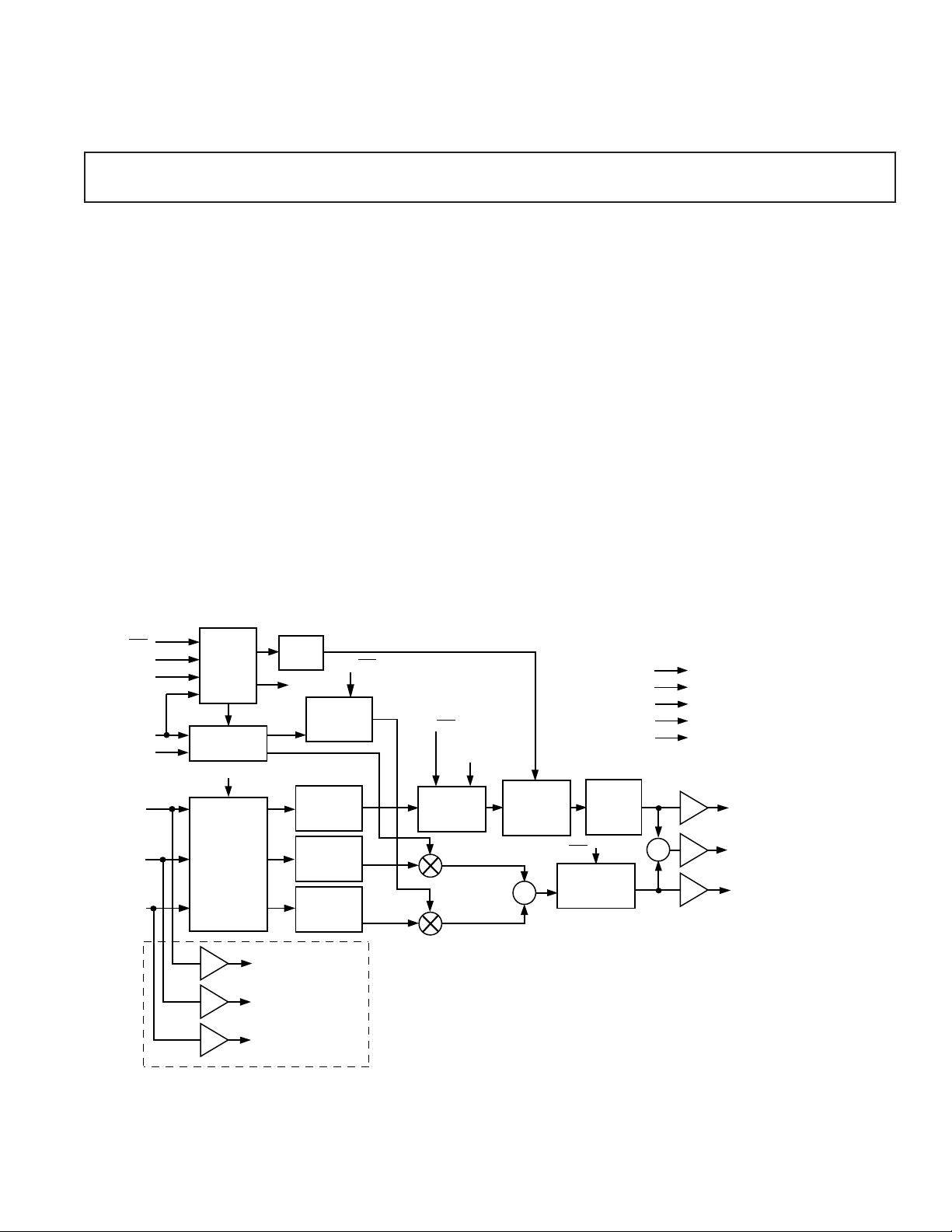
(continued from page 1)
All required low-pass filters are on chip. After the input signals
pass through a precision RGB to YUV encoding matrix, two onchip low-pass filters limit the bandwidth of the U and V color
difference signals to 1.2 MHz prior to quadrature modulation of
the color subcarrier; a third low-pass filter at 3.6 MHz (NTSC)
or 4.4 MHz (PAL) follows the modulators to limit the harmonic
content of the output.
Delays in the U and V chroma filters are matched by an on-chip
sampled data delay line in the Y signal path; to prevent aliasing,
prefilter at 5 MHz is included ahead of the delay line and a post
filter at 5 MHz is added after the delay line to suppress harmonics in the output. These low-pass filters are optimized for minimum pulse overshoot. The overall delay is about 170ns, which
precompensates for delays in the filters used to decode the
NTSC or PAL signal in a television receiver. (This precompensation delay is already present in TV broadcasts.)
The AD720 and AD721 are available in a 28-pin plastic leaded
chip carrier for the 0°C to +70°C commercial temperature range.
THEORY OF OPERATION
Referring to the AD720/AD721 block diagram (Figure 8), the
RGB inputs (each 0 mV to 714 mV in NTSC or 0 mV to
700 mV in PAL) are first encoded into luminance and color
difference signals. The luminance signal is called the “Y”
signal and the color-difference signals are called U and V. The
RGB inputs are encoded into the YUV format using the
transformation
Y = 0.299R + 0.587G + 0.114B
U = 0.493 (B-Y)
V = 0.877 (R-Y)
For NTSC operation, the chroma amplitude is increased by the
factor 1.06 prior to summation with the luminance output. The
burst signal is inserted into the Y channel in the encoding matrix.
The three outputs of the encoding matrix, now transformed into Y,
U, and V components, take two paths. The Y (luminance) signal is
passed through a delay line consisting of a prefilter, a sampled-data
delay line, and a post filter. The pre- and post-filters prevent
aliasing of harmonics back into the baseband video. The overall delay is a nominal –170 ns relative to the chrominance signal, in
keeping with broadcast requirements to compensate for delays introduced by the filters in the decoding process.
The U and V components pass through 4-pole modified Bessel
low-pass filters with a 1.2 MHz –3 dB frequency to prevent
aliasing in the balanced modulators, where they modulate a
3.579 545 000 MHz (NTSC) or 4.433 618 750 MHz (PAL)
signal via a pair of balanced modulators driven in quadrature by
the color subcarrier.
The AD720/AD721 4FSC input drives a digital divide-by-4 circuit (two flip-flops) to create the quadrature signal. The reference phase 0° is used for the U signal. In the NTSC mode, the
V signal is modulated at 90°, but in the PAL mode, the V
modulation input alternates between 90° and 270° at half the
line rate as required by the PAL standard. The outputs of the
balanced modulators are summed and low-pass filtered to remove harmonics.
REV. 0
Figure 8. AD720/AD721 Functional Block Diagram
–5–
Page 6

AD720/AD721
The filtered output is summed with the luminance signal to create a composite video signal. The separate luminance, chrominance, and composite video signals are amplified by gain-of-two
amplifiers for driving 75 Ω reverse-terminated lines. The separate luminance and chrominance outputs together are known as
“S-Video.”
The digital section of the AD720/AD721 is clocked by the
4FSC input. It measures the width of pulses in the composite
sync input to separate vertical, horizontal, and serration pulses
and to insert the subcarrier burst only after a valid horizontal
sync pulse.
+5V FROM
ENCODE INPUT
ENCODE = CMOS HIGH
POWER DOWN = CMOS LOW
IOR
VIDEO
RAM-DAC
ADV47X
ADV71XX
VIDEO STANDARD
SELECTION INPUT
NTSC = CMOS HIGH
PAL = CMOS LOW
IOG
IOB
75Ω
75Ω
75Ω
ANALOG SUPPLY
AGND
5
ENCD
6
RDIN
75Ω
7
AGND
8
GRIN
75Ω
9
AGND
10
BLIN
75Ω
11
STND
AGND
+5V FROM
ANALOG SUPPLY
0.1µF
4 3 2 1 28 27 26
NC
NC
NC
AD720
RGB TO NTSC/PAL
ENCODER
APOS
CRMA
CMPS
0.1µF
Asserting the ENCD pin to a logical low routes the AD721’s
RGB inputs through three gain-of-two bypass buffers for driving
75 Ω reverse-terminated lines, bypassing the encoder section of
the AD721. The triple bypass amplifier is utilized to overcome
the loading effects of a “TV-out” connection on the RGB monitor output. When a video encoder is connected to outputs of a
current-out video RAMDAC or VGA controller, the R, G, and
B signals to the monitor are loaded-down. This requires the use
of a gain block to properly drive the monitor.
–5V FROM
ANALOG SUPPLY
0.1µF
VNEG
APOS
APOS
NC
LUMA
VNEG
DGND
DGND
18171615141312
SYNC
DPOS
ASNC
DPOS
4FSC
25
24
23
22
21
20
19
75Ω
75Ω
75Ω
COMPOSITE SYNC INPUT
CMOS LOGIC LEVEL
NEGATIVE SYNC TIPS
+5V FROM
0.1µF
0.1µF
0.1µF
DIGITAL SUPPLY
+5V FROM
DIGITAL SUPPLY
4 X SUBCARRIER INPUT
CMOS LOGIC LEVELS
NTCS = 14.318 180MHz
PAL = 17.734 480MHz
–5V FROM ANALOG SUPPLY
LUMINANCE OUTPUT
COMPOSITE OUTPUT
CHROMINANCE OUTPUT
ENCODE INPUT
ENCODE = CMOS HIGH
BYPASS = CMOS LOW
IOR
VIDEO
RAM-DAC
ADV47X
ADV71XX
VIDEO STANDARD
SELECTION INPUT
NTSC = CMOS HIGH
PAL = CMOS LOW
IOG
IOB
75Ω
75Ω
75Ω
75Ω
75Ω
75Ω
ANALOG SUPPLY
Figure 9. AD720 Application
NC
CMPS
0.1µF
+5V FROM
ANALOG SUPPLY
APOS
APOS
0.1µF
4 3 2 1 28 27 26
AGND
5
ENCD
6
RDIN
7
AGND
8
GRIN
9
AGND
10
BLIN
11
STND
+5V FROM
NC
RGB TO NTSC/PAL
CRMA
AGND
NC
AD721
ENCODER
APOS
VNEG
NC
LUMA
VNEG
DGND
SYNC
DPOS
ASNC
DPOS
DGND
18171615141312
4FSC
25
24
23
22
21
20
19
75Ω
75Ω
75Ω
75Ω
75Ω
75Ω
0.1µF
0.1µF
0.1µF
RED OUTPUT
GREEN OUTPUT
BLUE OUTPUT
–5V FROM
ANALOG SUPPLY
COMPOSITE SYNC INPUT
CMOS LOGIC LEVEL
NEGATIVE SYNC TIPS
+5V FROM
DIGITAL SUPPLY
+5V FROM
DIGITAL SUPPLY
4 X SUBCARRIER INPUT
0.1µF
CMOS LOGIC LEVELS
NTCS = 14.318 180MHz
PAL = 17.734 480MHz
–5V FROM ANALOG SUPPLY
LUMINANCE OUTPUT
COMPOSITE OUTPUT
CHROMINANCE OUTPUT
Figure 10. AD721 Application
–6–
REV. 0
Page 7

AD720/AD721
APPLYING THE AD720/AD721
Figure 9 shows the application of the AD720 and Figure 10
shows the application of the AD721. Note that the AD720 and
AD721 differ from other analog encoders because they are dc
coupled. This means that, for example, the expected RGB
inputs are 0 mV to 714 mV in NTSC and 0 mV to 700 mV in
PAL. The luminance, chrominance, and composite outputs
are also dc coupled. These outputs can drive a 75Ω reverseterminated load. Unused outputs should be terminated with
150 Ω resistors.
The RGB data must be supplied to the AD720/AD721 at
NTSC or PAL rates, interlaced format. Various VGA chip set
vendors support this mode of operation. Most computers supply
RGB outputs in noninterlaced format at higher data rates than
NTSC and PAL, which means that “outboard” encoders must
supply some form of timing conversion before the RGB data
reaches the AD720/AD721.
Note also that the AD720/AD721 does not have internal dc restoration and does not accept sync on green. The composite sync
input is a separate, CMOS logical-level input and must be synchronized with the 4FSC input, which serves as the master clock
for the AD720/AD721.
The AD720/AD721 does not implement two elements of the
PAL and NTSC standards. In NTSC operation, it does not
support the 7.5 IRE unit setup (1 IRE unit = 7.14 mV)—this
must be added via software using the RGB inputs. Many RAMDACs, such as the Analog Devices ADV471 and ADV478, offer
a logic-selectable setup mode. In PAL operation, the AD720/
AD721 does not implement a 25 Hz subcarrier offset.
Decoupling and Grounding
Referring to the pin descriptions, the AD720/AD721 uses multiple analog grounds, digital grounds, digital positive supply inputs, analog positive supply inputs, and analog negative supply
inputs in order to maximize isolation between analog and digital
signal paths.
The most sensitive input of the AD720/AD721 is the 4FSC pin:
any noise on this pin directly affects the subcarrier and causes
degradation of the picture. Digital and analog grounds should
be kept separate and brought together at a single point.
All power supply pins should be decoupled using 0.1µF ceramic
capacitors located as close to the AD720/AD721 as possible. In
addition, ferrite beads may be slipped over the power supply
leads to reduce high frequency noise.
If a high speed RAM-DAC is used (e.g., capable of 80MHz operation with subnanosecond rise times), care must be taken to
properly terminate the input printed-circuit-board traces to the
AD720/AD721. Otherwise, ringing on these traces may occur
and cause degradation of the picture.
APPLICATIONS HINTS
In applying the AD720/AD721, problems may arise due to incorrect input signals. A few common situations follow.
Fade to Black or White—Invalid Horizontal Sync Pulses
Some systems produce sync pulses that are longer or shorter
than the NTSC and PAL standards specify. The digital sync
separator in the AD720/AD721 ignores horizontal sync pulses
that are too long or too short. Figure 11 shows the timing windows for valid NTSC and PAL horizontal sync pulses.
NTSC: 5.30µs
PAL: 5.46µs
COLOR BURST
COMPOSITE SYNC PULSE
NTSC: 2.79µs
PAL: 3.21µs
IF THE TRAILING EDGE OF A COMPOSITE SYNC PULSE IS WITHIN
THIS WINDOW, THE PULSE IS TREATED AS A HORIZONTAL SYNC PULSE.
IF THE TRAILING EDGE IS OUTSIDE THIS WINDOW, THE PULSE IS TREATED
AS AN EQUALIZING OR BLANKING PULSE.
NTSC: 2.51µs
PAL: 2.25µs
NTSC: 2.51µs
PAL: 2.25µs
Figure 11. NTSC and PAL Timing for Valid Horizontal
Sync Pulses
When the horizontal sync pulses are too long or too short, a dc
offset voltage (due to charge storage) increases on the output of
the sampled data delay line’s auto-zero amplifier. Normally, this
offset voltage is removed at the beginning of every line, as signified by the horizontal sync pulse. Without the horizontal sync
pulse, the dc offset on the auto-zero amplifier increases over
time (usually about three to five minutes) until it overrides the
luminance information. The end result is a slow fade to black or
white.
Color Flickering—Asynchronous Operation
The AD720/AD721 requires that its 4FSC and composite sync
signals be synchronized. In most systems, when the two signals
are synchronized, the composite sync signal is generated using a
4FSC signal as the reference. After every four frames, the
AD720/AD721 resets the phase quadrature generator. When the
CSYNC and 4FSC are synchronized, this reset is transparent to
the system because the reference phase does not change. When
the CSYNC and 4FSC are not synchronized, the difference
between the reference phase and its new value upon reset causes
an instantaneous color shift, which appears as a flickering in the
color.
Adding NTSC Setup
The easiest way to add the 7.5 IRE unit1 setup is to use a
ADV471/478 or ADV477/475 or ADV473 type RAM-DAC,
which have a logic-selectable setup (called “pedestal” on some
data sheets and “setup” on others).
Color Fidelity
A source impedance other than 37.5 Ω (75 Ωi75 Ω—a
reverse-terminated 75 Ω input) can cause errors in the YUV
encoding matrix, which is basically resistive and depends on the
correct source impedance for accuracy. Figures 9 and 10 show
the correct interface between a RAM-DAC and the AD720 and
AD721 respectively, using 75 Ω reverse-terminated connections.
NOTE
1
IRE unit = 7.14 mV.
REV. 0
–7–
Page 8

AD720/AD721
0.048 (1.21)
0.042 (1.07)
0.050
(1.27)
BSC
(0.50)
OUTLINE DIMENSIONS
Dimensions shown in inches and (mm).
28-Lead Plastic Leaded Chip Carrier (PLCC) Package
P-28A
0.180 (4.57)
0.165 (4.19)
0.025 (0.63)
0.015 (0.38)
0.021 (0.53)
0.013 (0.33)
0.430 (10.92)
0.390 (9.91)
0.032 (0.81)
0.026 (0.66)
0.040 (1.01)
0.025 (0.64)
0.110 (2.79)
0.085 (2.16)
0.020
0.048 (1.21)
0.042 (1.07)
4
5
11
12
R
PIN 1
IDENTIFIER
TOP
VIEW
0.456 (11.58)
0.450 (11.43)
0.495 (12.57)
0.485 (12.32)
0.056 (1.42)
0.042 (1.07)
26
25
19
18
SQ
SQ
C1932–7.5–7/94
–8–
PRINTED IN U.S.A.
REV. 0
 Loading...