

Page 1
Ultralow Power, 1.8 V, 3 mm × 3 mm,
V
www.BDTIC.com/ADI
FEATURES
Ultralow power
Power supply voltage: 1.8 V to 3.6 V
Operation power supply current: 70 μA typical
Power-down current: 2 μA typical
Fast response time
Conversion time: 10 ms per channel
Wake-up time from serial interface: 300 μs
Adaptive environmental compensation
2 capacitance input channels
Sensor capacitance (C
Sensitivity up to 3 fF
2 modes of operation
Standalone with fixed settings
Interfaced to a microcontroller for user-defined settings
2 detection output flags
2-wire serial interface (I
Operating temperature: −40°C to +85°C
10-lead LFCSP package (3 mm × 3 mm × 0.8 mm)
APPLICATIONS
Buttons and switches
Proximity sensing
Contactless switching
Position detection
Level detection
Portable products
): 0 pF up to 13 pF
SENS
2
C-compatible)
2-Channel Capacitance Converter
AD7156
GENERAL DESCRIPTION
The AD7156 delivers a complete signal processing solution for
capacitive sensors, featuring an ultralow power converter with
fast response time.
The AD7156 uses an Analog Devices, Inc., capacitance-todigital converter (CDC) technology, which combines features
important for interfacing to real sensors, such as high input
sensitivity and high tolerance of both input parasitic ground
capacitance and leakage current.
The integrated adaptive threshold algorithm compensates for
any variations in the sensor capacitance due to environmental
factors like humidity and temperature or due to changes in the
dielectric material over time.
By default, the AD7156 operates in standalone mode using the
fixed power-up settings and indicates detection on two digital
outputs. Alternatively, the AD7156 can be interfaced to a microcontroller via the serial interface, the internal registers can be
programmed with user-defined settings, and the data and status
can be read from the part.
The AD7156 operates with a 1.8 V to 3.6 V power supply. It is
specified over the temperature range of −40°C to +85°C.
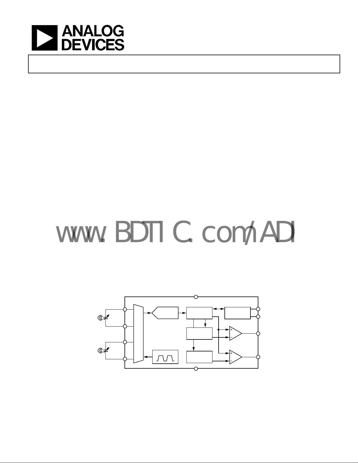
FUNCTIONAL BLOCK DIAGRAM
C
SENS1
C
SENS2
Rev. 0
Information furnished by Analog Devices is believed to be accurate and reliable. However, no
responsibility is assumed by Anal og Devices for its use, nor for any infringements of p atents or other
rights of third parties that may result from its use. Specifications subject to change without notice. No
license is granted by implication or otherwise under any patent or patent rights of Analog Devices.
Trademarks and registered trademarks are the property of their respective owners.
CIN1
EXC1
CIN2
EXC2
MUX
- CDC
AD7156
EXCITATION
DD
DIGITAL
FILTER
THRESHOLD
THRESHOLD
GND
Figure 1.
One Technology Way, P.O. Box 9106, Norwood, MA 02062-9106, U.S.A.
Tel: 781.329.4700 www.analog.com
Fax: 781.461.3113 ©2008 Analog Devices, Inc. All rights reserved.
SERIAL
INTERFACE
SCL
SDA
OUT1
OUT2
7726-001
Page 2

AD7156
www.BDTIC.com/ADI
TABLE OF CONTENTS
Features .............................................................................................. 1
Applications ....................................................................................... 1
General Description ......................................................................... 1
Functional Block Diagram .............................................................. 1
Revision History ............................................................................... 2
Specifications ..................................................................................... 3
Timing Specifications .................................................................. 5
Absolute Maximum Ratings ............................................................ 6
ESD Caution .................................................................................. 6
Pin Configuration and Function Descriptions ............................. 7
Typical Performance Characteristics ............................................. 8
Theory of Operation ...................................................................... 11
Capacitance-to-Digital Converter ............................................ 11
CAPDAC ..................................................................................... 11
Comparator and Threshold Modes .......................................... 12
Adaptive Threshold .................................................................... 12
Sensitivity..................................................................................... 12
Data Average ............................................................................... 13
Hysteresis ..................................................................................... 13
Timeout ........................................................................................ 13
Auto-DAC Adjustment .............................................................. 14
Power-Down Timer ................................................................... 14
Register Descriptions ..................................................................... 15
Status Register ............................................................................. 16
Data Registers ............................................................................. 17
Average Registers ........................................................................ 18
Fixed Threshold Registers ......................................................... 18
Sensitivity Registers ................................................................... 18
Timeout Registers ....................................................................... 18
Setup Registers ............................................................................ 19
Configuration Register .............................................................. 20
Power-Down Timer Register .................................................... 21
CAPDAC Registers .................................................................... 21
Serial Number Register .............................................................. 21
Chip ID Register ......................................................................... 21
Serial Interface ................................................................................ 22
Read Operation........................................................................... 22
Write Operation.......................................................................... 22
AD7156 Reset ............................................................................. 23
General Call ................................................................................ 23
Hardware Design Considerations ................................................ 24
Overview ..................................................................................... 24
Parasitic Capacitance to Ground .............................................. 24
Parasitic Resistance to Ground ................................................. 24
Parasitic Parallel Resistance ...................................................... 24
Parasitic Serial Resistance ......................................................... 25
Input Overvoltage Protection ................................................... 25
Input EMC Protection ............................................................... 25
Power Supply Decoupling and Filtering .................................. 25
Application Examples ................................................................ 26
Outline Dimensions ....................................................................... 27
Ordering Guide .......................................................................... 27
REVISION HISTORY
10/08—Revision 0: Initial Version
Rev. 0 | Page 2 of 28
Page 3

AD7156
www.BDTIC.com/ADI
SPECIFICATIONS
VDD = 1.8 V to 3.6 V, GND = 0 V, temperature range = −40°C to +85°C, unless otherwise noted.
Table 1.
Parameter Min Typ Max Unit
CAPACITIVE INPUT
2, 3
Conversion Input Range, CIN to EXC
3.2 4 pF 4 pF input range
1.6 2 pF 2 pF input range
0.8 1 pF 1 pF input range
0.4 0.5 pF 0.5 pF input range
Resolution
4, 5
2.0 fF 4 pF input range
1.6 fF 2 pF input range
1.4 fF 1 pF input range
1.0 fF 0.5 pF input range
4, 6
Maximum Allowed Capacitance, CIN to GND
Minimum Allowed Resistance, CIN to GND
Maximum Allowed Serial Resistance
4, 6
50 kΩ See Figure 14
4, 6
50 pF
10 MΩ See Figure 10 and Figure 11
Gain Error −20 +20 %
Gain Deviation over Temperature
Gain Matching Between Ranges
Offset Error
4
50 fF CIN and EXC pins disconnected
Offset Deviation over Temperature
Integral Nonlinearity (INL)
Channel-to-Channel Isolation
Power Supply Rejection
4
4 fF/V
4
0.5 %FSR See Figure 17
4
−2 +2 %
4
4
0.05 %
4
60 dB
5 fF
CAPDAC
Full Range 10 12.5 pF
Resolution (LSB)
Differential Nonlinearity (DNL)
Auto-DAC Increment/Decrement
4
200 fF
4
0.25 LSB
4, 7
25 75 % of C
EXCITATION
4, 7
Voltage
±VDD/2 V
Frequency 16 kHz See Figure 18
4, 6
Maximum Allowed Capacitance EXC to GND
Minimum Allowed Resistance EXC to GND
4, 6
1 MΩ See Figure 12 and Figure 13
1000 pF
LOGIC OUTPUTS (OUT1, OUT2)
Output Low Voltage (VOL) 0.4 V I
Output High Voltage (VOH) VDD – 0.6 V I
SERIAL INTERFACE INPUTS (SCL, SDA)
Input High Voltage (VIH) 70 % of VDD
Input Low Voltage (VIL) 25 % of VDD
Input Leakage Current ±0.1 ±5 µA
Input Pin Capacitance 6 pF
OPEN-DRAIN OUTPUT (SDA)
Output Low Voltage (VOL) 0.4 V
Output High Leakage Current (IOH) 0.1 5 µA V
1
range
IN
Test Conditions/Comments
See Figure 4, Figure 5, and
Figure 6
CIN and EXC pins disconnected
See Figure 16
See Figure 7, Figure 8, and
= −3 mA
SINK
= +3 mA
SOURCE
= −6.0 mA
SINK
= VDD
OUT
Figure 9
I
Rev. 0 | Page 3 of 28
Page 4

AD7156
www.BDTIC.com/ADI
Parameter Min Typ Max Unit
1
Test Conditions/Comments
POWER REQUIREMENTS
VDD-to-GND Voltage 1.8 3.6 V
IDD Current
4, 8
65 75 µA V
≤ 2.7 V, see Figure 20
DD
70 85 µA VDD = 3.6 V, see Figure 20
IDD Current Power-Down Mode
4, 8
2 10 µA V
≤ 2.7 V, see Figure 21
DD
2 17 µA VDD = 3.6 V, see Figure 21
1
Capacitance units: 1 pF = 1 × 10
2
The CAPDAC can be used to shift (offset) the input range. The total capacitance of the sensor can therefore be up to the sum of the CAPDAC value and the conversion
input range. With the auto-DAC feature, the CAPDAC is adjusted automatically when the CDC input value is lower than 25% or higher than 75% of the CDC nominal
input range.
3
The maximum capacitance of the sensor connected between the EXCx and CINx pins is equal to the sum of the minimum guaranteed value of the CAPDAC and the
minimum guaranteed input range.
4
The maximum specification is not production tested but is supported by characterization data at initial product release.
5
The resolution of the converter is not limited by the output data format or output data LSB (least significant bit) size, but by the converter and system noise level. The
noise-free resolution is defined as level of peak-to-peak noise coming from the converter itself, with no connection to the CIN and EXC pins.
6
These specifications are understood separately. Any combination of the capacitance to ground and serial resistance may result in additional errors, for example gain
error, gain drift, offset error, offset drift, and power supply rejection.
7
Specification is not production tested but is guaranteed by design.
8
Digital inputs equal to VDD or GND.
−12
F; 1 fF = 10
−15
F.
Rev. 0 | Page 4 of 28
Page 5
AD7156
www.BDTIC.com/ADI
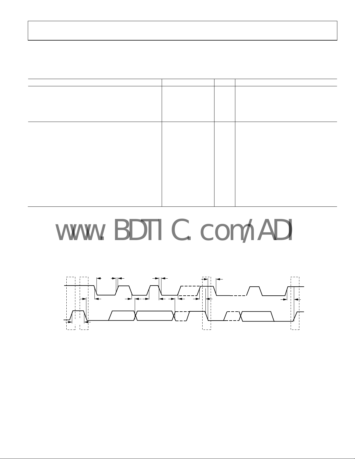
TIMING SPECIFICATIONS
VDD = 1.8 V to 3.6 V, GND = 0 V, Input Logic 0 = 0 V, Input Logic 1 = VDD, temperature range = −40°C to +85°C, unless otherwise noted.
Table 2.
Parameter Min Typ Max Unit Test Conditions/Comments
CONVERTER
Conversion Time
Wake-Up Time from Power-Down Mode
Power-Up Time
Reset Time
SERIAL INTERFACE
SCL Frequency 0 400 kHz
SCL High Pulse Width, t
SCL Low Pulse Width, t
SCL, SDA Rise Time, tR 0.3 µs
SCL, SDA Fall Time, t
Hold Time (Start Condition), t
Setup Time (Start Condition), t
Data Setup Time, t
Setup Time (Stop Condition), t
Data Hold Time (Master), t
Bus-Free Time (Between Stop and Start Conditions), t
1
Conversion time is 304 internal clock cycles for both channels (nominal clock 16 kHz); the internal clock frequency is equal to the specified excitation frequency.
2
Specification is not production tested but is supported by characterization data at initial product release.
3
Wake-up time is the maximum delay between the last SCL edge writing the configuration register and the start of conversion.
4
Power-up time is the maximum delay between the VDD crossing the minimum level (1.8 V) and either the start of conversion or when ready to receive a serial
interface command.
5
Reset time is the maximum delay between the last SCL edge writing the reset command and either the start of conversion or when ready to receive a serial
interface command.
6
Sample tested during initial release to ensure compliance.
7
All input signals are specified with input rise/fall times = 3 ns, measured between the 10% and 90% points. Timing reference points at 50% for inputs and outputs.
Output load = 10 pF.
1
2, 3
2, 4
2 ms
2, 5
6, 7
0.6 µs
HIGH
1.3 µs
LOW
F
0.6 µs After this period, the first clock is generated.
HD;STA
SU;STA
0.1 µs
SU;DAT
SU;STO
10 ns
HD;DAT
t
LOW
0.3 ms
0.6 µs Relevant for repeated start condition.
0.6 µs
t
R
20 ms Both channels, 10 ms per channel.
2 ms
See Figure 2.
0.3 µs
1.3 µs
BUF
t
F
t
HD;STA
SCL
SDA
t
t
BUF
PS
HD;STA
t
HD;DAT
t
HIGH
t
SU;DAT
t
SU;STA
S
Figure 2. Serial Interface Timing Diagram
Rev. 0 | Page 5 of 28
t
SU;STO
P
07726-002
Page 6
AD7156
www.BDTIC.com/ADI
ABSOLUTE MAXIMUM RATINGS
TA = 25°C, unless otherwise noted.
Table 3.
Parameter Rating
Positive Supply Voltage VDD to GND
Voltage on Any Input or Output to GND –0.3 V to VDD + 0.3 V
ESD Rating
ESD Association Human Body Model, S5.1
Field-Inducted Charged Device Model
Operating Temperature Range −40°C to +85°C
Storage Temperature Range –65°C to +150°C
Maximum Junction Temperature 150°C
LFCSP Package
θJA, Thermal Impedance to Air
θJC, Thermal Impedance to Case
Reflow Soldering (Pb-Free)
Peak Temperature 260(0/−5)°C
Time at Peak Temperature 10 sec to 40 sec
−0.3 V to +3.9 V
4 kV
500 V
49°C/W
3°C/W
Stresses above those listed under Absolute Maximum Ratings
may cause permanent damage to the device. This is a stress
rating only; functional operation of the device at these or any
other conditions above those indicated in the operational
section of this specification is not implied. Exposure to absolute
maximum rating conditions for extended periods may affect
device reliability.
ESD CAUTION
Rev. 0 | Page 6 of 28
Page 7
AD7156
www.BDTIC.com/ADI
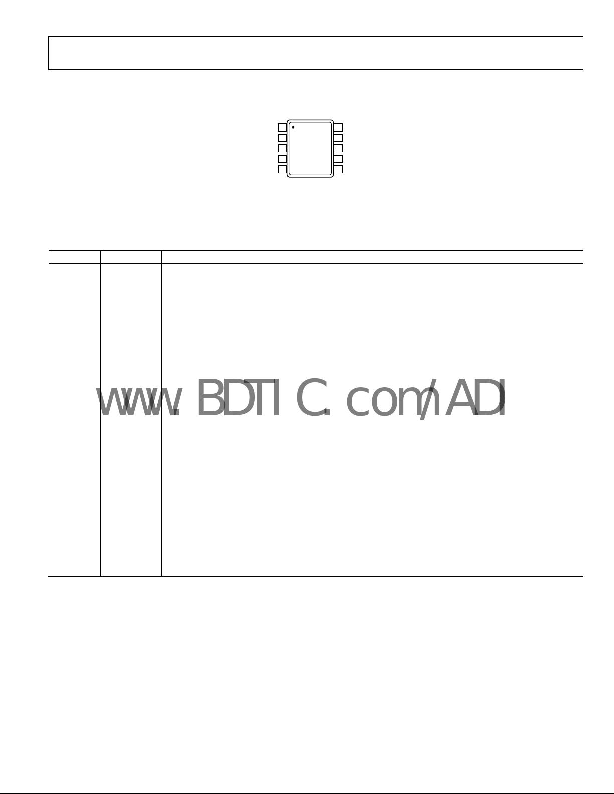
PIN CONFIGURATION AND FUNCTION DESCRIPTIONS
1
GND
VDD
2
CIN2
CIN1
EXC2
NOTES
1. THE EXPOSED PAD MUST BE CONNECTED TO
GND OR IT MUST BE ISOLATED (FLOATING).
AD7156
3
TOP VIEW
(Not to Scale)
4
5
Figure 3. Pin Configuration
Table 4. Pin Function Descriptions
Pin No. Mnemonic Description
1 GND Ground Pin.
2 VDD
Power Supply Voltage. This pin should be decoupled to GND using a low impedance capacitor, such as a
0.1 F X7R multilayer ceramic capacitor.
3 CIN2
CDC Capacitive Input Channel 2. The measured capacitance (sensor) is connected between the EXC2 pin and
the CIN2 pin. If not used, this pin can be left open circuit or be connected to GND. When a conversion is
performed on Channel 2, the CIN2 pin is internally connected to a high impedance input of the Σ-∆
modulator. When a conversion is performed on the other channel or in idle mode or power-down mode,
the CIN2 pin is internally disconnected and left floating by the part.
4 CIN1
CDC Capacitive Input Channel 1. The measured capacitance (sensor) is connected between the EXC1 pin and
the CIN1 pin. If not used, this pin can be left open circuit or be connected to GND. When a conversion is
performed on Channel 1, the CIN1 pin is internally connected to a high impedance input of the Σ-∆
modulator. When a conversion is performed on the other channel or in idle mode or power-down mode,
the CIN1 pin is internally disconnected and left floating by the part.
5 EXC2
CDC Excitation Output Channel 2. The measured capacitance is connected between the EXC2 pin and the
CIN2 pin. If not used, this pin should be left as an open circuit. When a conversion is performed on Channel 2,
the EXC2 pin is internally connected to the output of the excitation signal driver. When a conversion is performed on the other channel or in idle mode or power-
to GND.
6 EXC1
CDC Excitation Output Channel 1. The measured capacitance is connected between the EXC1 pin and the
CIN1 pin. If not used, this pin should be left as an open circuit. When a conversion is performed on Channel 1,
the EXC1 pin is internally connected to the output of the excitation signal driver. When a conversion is performed on the other channel or in idle mode or power-
to GND.
7 OUT1 Logic Output Channel 1. A high level on this output indicates proximity detected on CIN1.
8 OUT2 Logic Output Channel 2. A high level on this output indicates proximity detected on CIN2.
9 SCL
Serial Interface Clock Input. This pin connects to the master clock line and requires a pull-up resistor if not
provided elsewhere in the system.
10 SDA
Serial Interface Bidirectional Data. This pin connects to the master data line and requires a pull-up resistor if
not provided elsewhere in the system.
10
SDA
SCL
9
OUT2
8
7
OUT1
EXC1
6
07726-003
down mode, the EXC2 pin is internally connected
down mode, the EXC1 pin is internally connected
Rev. 0 | Page 7 of 28
Page 8
AD7156
www.BDTIC.com/ADI
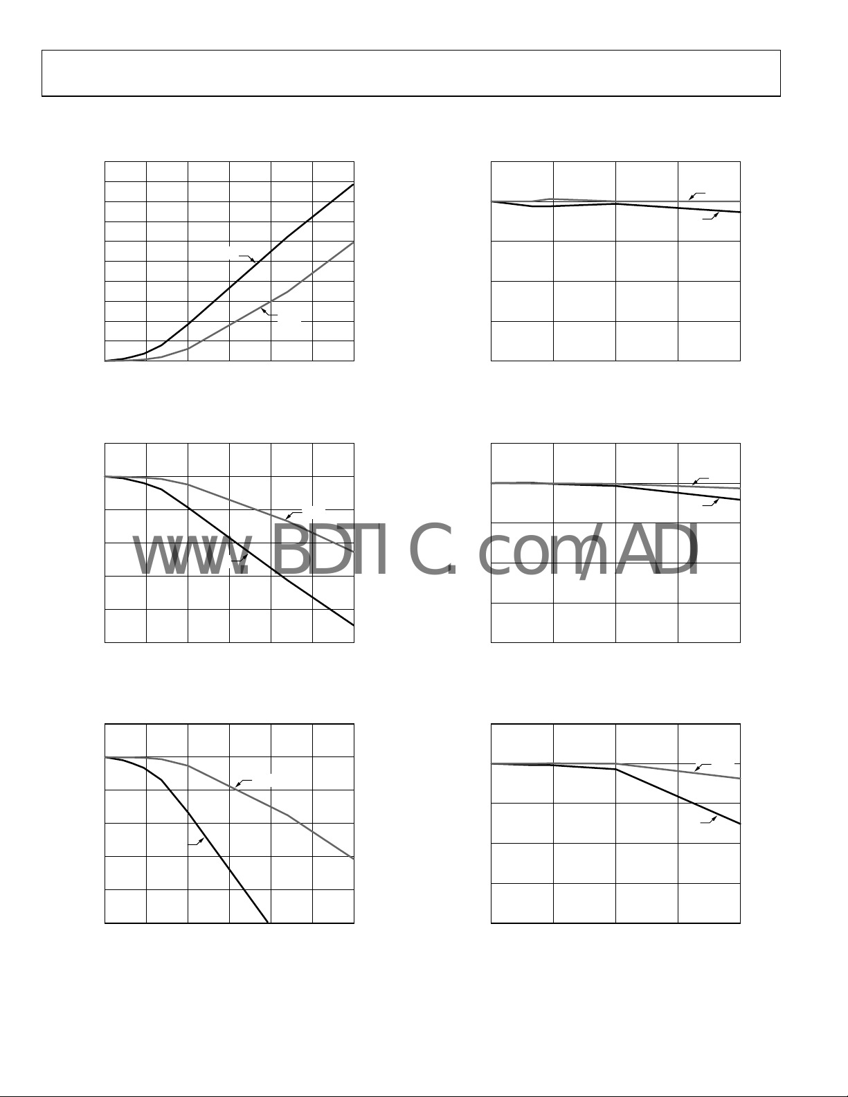
TYPICAL PERFORMANCE CHARACTERISTICS
2.0
1.8
1.6
1.4
1.2
1.0
0.8
OFFSET ERROR (pF)
0.6
0.4
0.2
0
0 50 100 150 200 250 300
CAPACITANCE CIN T O GROUND (pF )
1.8V
3.3V
Figure 4. Capacitance Input Offset Error vs. Capacitance CIN to GND,
= 1.8 V and 3.3 V, EXC Pin Open Circuit
V
DD
5
0
–5
–10
1.8V
–15
GAIN ERROR (%F SR)
–20
3.3V
1
0
–1
–2
OFFSET ERROR (fF)
–3
07726-004
–4
0 500 1000 1500 2000
CAPACITANCE EXC TO GROUND (pF )
3.3V
1.8V
07726-007
Figure 7. Capacitance Input Offset Error vs. Capacitance EXC to GND,
VDD = 1.8 V and 3.3 V, CIN Pin Open Circuit
1
0
–1
–2
GAIN ERROR (%F SR)
–3
3.3V
1.8V
–25
0 50 100 150 200 250 300
CAPACITANCE CIN T O GROUND (pF )
Figure 5. Capacitance Input Gain Error vs. Capacitance CIN to GND,
= 1.8 V and 3.3 V, CIN to EXC = 3 pF
V
DD
5
0
–5
–10
–15
GAIN ERROR (%F SR)
–20
–25
0 50 100 150 200 250 300
1.8V
CAPACITANCE CIN T O GROUND (pF )
3.3V
Figure 6. Capacitance Input Gain Error vs. Capacitance CIN to GND,
= 1.8 V and 3.3 V, CIN to EXC = 9 pF
V
DD
07726-005
07726-006
Rev. 0 | Page 8 of 2
–4
0 500 1000 1500 2000
CAPACITANCE EXC TO GROUND (pF )
Figure 8. Capacitance Input Gain Error vs. Capacitance EXC to GND,
VDD = 1.8 V and 3.3 V, CIN to EXC = 3 pF
1
0
–1
–2
GAIN ERROR (%F SR)
–3
–4
0 500 1000 1500 2000
CAPACITANCE EXC TO GROUND (pF )
3.3V
1.8V
Figure 9. Capacitance Input Gain Error vs. Capacitance EXC to GND,
= 1.8 V and 3.3 V, CIN to EXC = 9 pF
V
DD
8
07726-008
07726-009
Page 9
AD7156
www.BDTIC.com/ADI
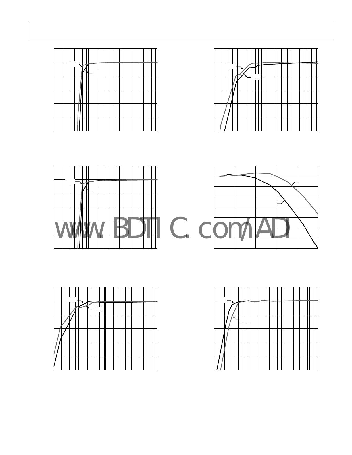
2
0.2
0
3.3V
–2
–4
–6
GAIN ERROR (%F SR)
–8
–10
1 10 100 1k
1.8V
RESISTANCE CIN T O GND (M)
Figure 10. Capacitance Input Gain Error vs. Resistance CIN to GND,
= 1.8 V and 3.3 V, CIN to EXC = 3 pF
V
DD
2
0
3.3V
–2
–4
–6
GAIN ERROR (%F SR)
–8
–10
1 10 100 1k
1.8V
RESISTANCE CI N TO GND (M)
Figure 11. Capacitance Input Gain Error vs. Resistance CIN to GND,
= 1.8 V and 3.3 V, CIN to EXC = 9 pF
V
DD
0
–0.2
–0.4
–0.6
GAIN ERROR (%F SR)
–0.8
07726-010
–1.0
3.3V
1.8V
07726-013
0.1 1 10 100 1k
RESISTANCE EXC TO GROUND (M )
Figure 13. Capacitance Input Gain Error vs. Resistance EXC to GND,
= 1.8 V and 3.3 V, CIN to EXC = 9 pF
V
DD
1
0
–1
–2
–3
–4
GAIN ERROR (%F SR)
–5
1
07726-01
–6
–7
0 20406080100
SERIAL RESI STANCE (k)
1.8V
3.3V
07726-014
Figure 14. Capacitance Input Gain Error vs. Serial Resistance,
= 1.8 V and 3.3 V, CIN to EXC = 3 pF
V
DD
0.2
0
–0.2
–0.4
–0.6
GAIN ERROR (%F SR)
–0.8
–1.0
1.8V
3.3V
0.1 1 10 100 1k
RESISTANCE EXC TO GROUND (M )
Figure 12. Capacitance Input Gain Error vs. Resistance EXC to GND,
= 1.8 V and 3.3 V, CIN to EXC = 3 pF
V
DD
2
07726-01
10
1.8V
0
–10
–20
–30
GAIN ERROR (%F SR)
–40
–50
1 10 100 1k
Figure 15. Capacitance Input Gain Error vs. Parallel Resistance,
= 1.8 V and 3.3 V, CIN to EXC = 3 pF
V
DD
Rev. 0 | Page 9 of 28
3.3V
07726-015
PARELLEL RE SISTANCE (M)
Page 10

AD7156
www.BDTIC.com/ADI
5
4
3
2
1
0
–1
OFFSET ERROR (fF)
–2
–3
–4
–5
–50 –25 500 25 75 100
TEMPERATURE (°C)
3.3V
Figure 16. Capacitance Input Offset Error vs. Temperature,
= 1.8 V and 3.3 V, CIN and EXC Pins Open Circuit
V
DD
1.8V
07726-016
20
10
0
DNL (fF)
–10
–20
010 205152530
Figure 19. CAPDAC Differential Nonlinearity (DNL), V
CAPDAC CODE
= 1.8 V
DD
07726-019
0.35
0.25
0.15
0.05
–0.05
GAIN ERROR (%F SR)
–0.15
–0.25
–0.35
–50 0 50 100
TEMPERATURE (°C)
Figure 17. Capacitance Input Gain Error vs. Temperature,
= 2.7 V, CIN to EXC = 4 pF
V
DD
16.50
16.25
16.00
15.75
15.50
15.25
FREQUENCY (kHz)
15.00
14.75
14.50
–50 0 50–25 25 75 100
1.8V
2.7V
2V
3.6V
TEMPERATURE ( °C)
Figure 18. EXC Frequency Error vs. Temperature,
= 1.8 V, 2 V, 2.7 V, and 3.6 V
V
DD
7
07726-01
8
07726-01
80
3.6V
70
2.7V
60
MAX (µA)
DD
I
1.8V
50
40
–50 0 50–25 25 75
2V
TEMPERATURE (° C)
Figure 20. Current vs. Temperature,
VDD = 1.8 V, 2 V, 2.7 V, and 3.6 V
4.0
3.5
3.0
2.5
2.0
MAX (µA)
DD
I
1.5
1.0
0.5
0
–50 0 50–25 25 75
3.6V
2.7V
2V
TEMPERATURE (°C)
Figure 21. Power-Down Current vs. Temperature,
VDD = 1.8 V, 2 V, 2.7 V, and 3.6 V
07726-020
1.8V
07726-021
Rev. 0 | Page 10 of
28
Page 11

AD7156
V
www.BDTIC.com/ADI
THEORY OF OPERATION
3.3
VDD
AD7156
CIN1
C
X1
EXC1
MUX
CIN2
C
X2
EXC2
CLOCK
GENERATOR
- CDC
CAPDAC
EXCITATION
POWER-DOWN
THRESHOLD
THRESHOLD
Figure 22. AD7156 Block Diagram
The AD7156 core is a high performance capacitance-to-digital
converter (CDC) that allows the part to be interfaced directly
to a capacitive sensor.
The comparators compare the CDC results with thresholds, either
fixed or dynamically adjusted by the on-chip adaptive threshold
algorithm engine. Thus, the outputs indicate a defined change in
the input sensor capacitance.
The AD7156 also integrates an excitation source, CAPDAC
for the capacitive inputs, an input multiplexer, a complete clock
generator, a power-down timer, a power supply monitor, control
logic, and an I
2
C®-compatible serial interface for configuring the
part and accessing the internal CDC data and status, if required
in the system (see Figure 22).
CAPACITANCE-TO-DIGITAL CONVERTER
Figure 23 shows the CDC simplified functional diagram. The
converter consists of a second-order Σ-Δ charge balancing
modulator and a third-order digital filter. The measured
capacitance C
and the Σ-Δ modulator input. The excitation signal is applied
on the C
continuously samples the charge going through the C
digital filter processes the modulator output, which is a stream
of 0s and 1s containing the information in 0 and 1 density. The
data is processed by the adaptive threshold engine and output
comparators; the data can also be read through the serial interface.
The AD7156 is designed for floating capacitive sensors.
Therefore, both C
or any other fixed potential node in the system.
The AD7156 features slew rate limiting on the excitation voltage
output, which decreases the energy of higher harmonics on the
excitation signal and dramatically improves the system electromagnetic compatibility (EMC).
is connected between an excitation source
X
capacitor during the conversion, and the modulator
X
. The
X
plates have to be isolated from ground
X
TIMER
DIGITAL
FILTER
GND
SCL
SERIAL
INTERFACE
CIN
C
X
0pF TO 4pF
EXC
PROGRAMMING
SDA
INTERFACE
OUT1
DIGITAL
OUTPUTS
OUT2
7726-030
CAPACITANCE-TO -DIGIT AL CONVERTE R
CLOCK
GENERATOR
-
MODULATOR
EXCITATION
(CDC)
0x0000 TO 0xFFF0
DIGITAL
FILTER
DATA
07726-031
Figure 23. CDC Simplified Block Diagram
CAPDAC
The AD7156 CDC core maximum full-scale input range is 0 pF
to 4 pF. However, the part can accept a higher input capacitance,
caused, for example, by a nonchanging offset capacitance of up to
10 pF. This offset capacitance can be compensated for by using
the programmable on-chip CAPDAC.
CAPDAC
10pF
CIN
C
X
10pF TO 14pF
EXC
Figure 24. Using a CAPDAC
The CAPDAC can be understood as a negative capacitance
connected internally to a CIN pin. The CAPDAC has a 6-bit
resolution and a monotonic transfer function. Figure 24 shows
how to use the CAPDAC to shift the CDC 0 pF to 4 pF input
range to measure capacitance between 10 pF and 14 pF.
0x0000 TO 0xFFF0
0pF TO 4pF
DATA
07726-032
Rev. 0 | Page 11 of 28
Page 12

AD7156
CA
A
A
www.BDTIC.com/ADI
COMPARATOR AND THRESHOLD MODES
The AD7156 comparators and their thresholds can be
programmed to operate in two modes: fixed and adaptive
threshold modes. In an adaptive mode, the threshold
is dynamically adjusted and the comparator output indicates
fast changes and ignores slow changes in the input (sensor)
capacitance. Alternatively, the threshold can be programmed
as a constant (fixed) value, and the output then indicates any
change in the input capacitance that crosses the defined fixed
threshold.
The AD7156 logic output (active high) indicates either a positive or
a negative change in the input capacitance, in both adaptive and
fixed threshold modes (see Figure 25 and Figure 26).
POSITI VE CHANGE
POSITIVE
THRESHOLD
INPUT
CAPACITANCE
OUTPUT
Figure 25. Positive Threshold Mode
Indicates Positive Change in Input Capacitance
INPUT
PACITANCE
NEGATIVE
THRESHOLD
OUTPUT
Figure 26. Negative Threshold Mode
Indicates Negative Change in Input Capacitance
Additionally, for the adaptive mode only, the comparators can
work as window comparators, indicating input either inside or
outside a selected sensitivity band (see Figure 27 and Figure 28).
POSITIVE
THRESHOLD
INPUT CAPACIT ANCE
NEGATIVE
THRESHOLD
OUTPUT
Figure 27. In-Window (Adaptive) Threshold Mode
INPUT INSI DE THRESHOL D WINDOW
OUTPUT ACTIVE
OUTPUT ACTIVE
TIME
NEGATIVE CHANGE
OUTPUT ACTIVE
TIME
TIME
07726-033
07726-034
INPUT OUTSIDE THRESHOLD WINDOW
POSITIVE
THRESHOLD
INPUT CAPACIT ANCE
NEGATIVE
THRESHOLD
OUTPUT
OUTPUT ACTI VE
TIME
07726-036
Figure 28. Out-Window (Adaptive) Threshold Mode
ADAPTIVE THRESHOLD
In an adaptive mode, the thresholds are dynamically adjusted,
ensuring indication of fast changes (for example, an object
moving close to a capacitive proximity sensor) and eliminating
slow changes in the input (sensor) capacitance, usually caused
by environment changes such as humidity or temperature or
changes in the sensor dielectric material over time (see Figure 29).
FAST CHANGE
INPUT C
PACITANCE
THRESHOLD
OUTPUT ACTIVE
OUTPUT
Figure 29. Adaptive Threshold Indicates Fast Changes and Eliminates Slow
Changes in Input Capacitance
SLOW CHANGE
TIME
07726-037
SENSITIVITY
In adaptive threshold mode, the output comparator threshold
is set as a defined distance (sensitivity) above the data average,
below the data average, or both, depending on the selected
threshold mode of operation (see Figure 30). The sensitivity
value is programmable in the range of 0 LSB to 255 LSB of the
12-bit CDC converter (see the Register Descriptions section).
DAT
POSITIVE
THRESHOLD
DATA AVERAGE
NEGATIVE
THRESHOLD
OUTPUT ACTIVE
TIME
Figure 30. Threshold Sensitivity
07726-035
SENSITIVITY
SENSITIVITY
7726-039
Rev. 0 | Page 12 of 28
Page 13

AD7156
−
A
AAV
A
www.BDTIC.com/ADI
DATA AVERAGE
The adaptive threshold algorithm is based on an average calculated
from the previous CDC output data, using the following equation:
)1()(
+−=
NAverageNAverage
−
+
gThrSettlin
2
where:
Av erag e (N) is the new average value.
Av erag e (N − 1) is the average value from the previous cycle.
Data(N) is the latest complete CDC conversion result.
ThrSettling is a parameter, programmable in the setup registers.
A more specific case of the input capacitance waveform is a step
change. The response of the average to an input capacitance step
change (more exactly, response to a step change in the CDC output
data) is an exponential settling curve, which can be characterized
by the following equation:
/TimeConstN
eChangeAverageNAverage −+=
where:
Av erag e (N) is the value of average N complete CDC conversion
cycles after a step change on the input.
Av erag e (0) is the value before the step change.
TimeConst = 2
(ThrSettling + 1)
ThrSettling is a parameter, programmable in the setup registers.
See Figure 31 and the Register Descriptions section for further
information.
INPUT CAPACITANCE
(CDC DATA) CHANGE
)1()(
NAverageNData
1
)1()0()(
TIMEOUT
In the case of a large, long change in the capacitive input, when
the data average adapting to a new condition takes too long, a
timeout can be set.
The timeout becomes active (counting) when the CDC data
goes outside the band of data average ± sensitivity. When the
timeout elapses (a defined number of CDC conversions is
counted), the data average (and thus the thresholds), is forced
to follow the new CDC data value immediately (see Figure 33).
The timeout can be set independently for approaching (for change
in data toward the threshold) and for receding (for change in data
away from the threshold). See Figure 34, Figure 35, and the Register
Descriptions section for further information.
DAT
ERAGE
+ SENSITIVITY
DATA AVERAGE
DATA AVERAGE
– SENSITIVITY
Figure 33. Threshold Timeout After a Large Change in CDC Data
INPUT
CAPACITANCE
THRESHOLD
DATA AVERAGE
TIMEO UT APPROACHING
LARGE CHANGE IN DATA
TIMEOUT
TIME
07726-041
DATA AVERAGE RESPONSE
TIME
Figure 31. Data Average Response to Data Step Change
07726-038
HYSTERESIS
In adaptive threshold mode, the comparator features hysteresis.
The hysteresis is fixed to ¼ of the threshold sensitivity and can
be programmed on or off. The comparator does not have hysteresis in the fixed threshold mode.
DAT
POSITIVE
THRESHOLD
DATAAVERAGE
OUTPUT ACTIV E
OUTPUT
Figure 32. Threshold Hysteresis
TIME
HYSTERSIS
07726-040
OUTPUT ACT IVE
OUTPUT
Figure 34. Approaching Timeout in Negative Threshold Mode
Shortens False Output Trigger
TIME
07726-042
TIMEOUT RECEDING
LARGE CHANGE
INPUT
C
PACITANCE
THRESHOLD
OUTPUT ACTIVE
OUTPUT
TIME
Figure 35. Positive Timeout in Negative Threshold Mode
Shortens Period of Missing Output Trigger
7726-043
Rev. 0 | Page 13 of 28
Page 14

AD7156
www.BDTIC.com/ADI
AUTO-DAC ADJUSTMENT
In adaptive threshold mode, the part can dynamically adjust the
CAPDAC to keep the CDC in an optimal operating capacitive
range. When the auto-DAC function is enabled, the CAPDAC
value is automatically incremented when the data average
exceeds ¾ of the CDC full range (average > 0xA800), and
the CAPDAC value is decremented when the data average
goes below ¼ of the CDC full range (average < 0x5800).
The auto-DAC increment or decrement step depends on
the selected CDC capacitive input range (see the Setup Registers
section).
When the CAPDAC value reaches 0, the ¼ threshold for further
decrementing is ignored. Similarly, when the CAPDAC value
reaches its full range, the ¾ threshold is ignored. The CDC and
the rest of the algorithm are continuously working, and they are
functional down to a capacitance input of 0 pF or as high as the
capacitance input of (CAPDAC full range + CDC full range),
respectively.
POWER-DOWN TIMER
In power sensitive applications, the AD7156 can be set to
automatically enter power-down mode after a programmed
period of time in which the outputs have not been activated.
The AD7156 can then be returned to a normal operational
mode either via the serial interface or by the power supply
off/on sequence.
Rev. 0 | Page 14 of 28
Page 15

AD7156
www.BDTIC.com/ADI
REGISTER DESCRIPTIONS
Table 5. Register Summary1
Addr Pointer
Register
Status 0 0x00 R PwrDown
Ch 1 Data High 1 0x01 R 0x00
Ch 1 Data Low 2 0x02 R 0x00
Ch 2 Data High 3 0x03 R 0x00
Ch 2 Data Low 4 0x04 R 0x00
Ch 1 Average High 5 0x05 R 0x00
Ch 1 Average Low 6 0x06 R 0x00
Ch 2 Average High 7 0x07 R 0x00
Ch 2 Average Low 8 0x08 R 0x00
R/W Bit 7 Bit 6 Bit 5 Bit 4 Bit 3 Bit 2 Bit 1 Bit 0 Dec Hex
DacStep2
OUT2
DacStep1
OUT1 C1/C2
RDY2
(0) (1) (0) (1) (0) (0) (1) (1)
RDY1
Ch 1 Sensitivity/
Ch 1 Threshold High
Ch 1 Timeout/
Ch 1 Threshold Low
Ch 1 Setup 11 0x0B R/W RngH1 RngL1
Ch 2 Sensitivity/
Ch 2 Threshold High
Ch 2 Timeout/
Ch 2 Threshold Low
Ch 2 Setup 14 0x0E R/W RngH2 RngL2
Configuration 15 0x0F R/W ThrFixed ThrMD1 ThrMD0 EnCh1 EnCh2 MD2 MD1 MD0
Power-Down Timer 16 0x10 R/W Power-down timeout (6-bit value)
Ch 1 CAPDAC 17 0x11 R/W DacEn1 DacAuto1 DacValue1 (6-bit value)
Ch 2 CAPDAC 18 0x12 R/W DacEn2 DacAuto2 DacValue2 (6-bit value)
Serial Number 3 19 0x13 R Serial number—Byte 3 (MSB)
Serial Number 2 20 0x14 R Serial number—Byte 2
9 0x09 R/W Ch 1 sensitivity (in adaptive threshold mode)/Ch 1 threshold high byte (in fixed threshold mode)
0x08
10 0x0A R/W Ch 1 timeout (in adaptive threshold mode)/CH 1threshold low byte (in fixed threshold mode)
0x86
Hyst1
(0) (0) (0) (0) (0x0B)
12 0x0C R/W Ch 2 sensitivity (in adaptive threshold mode)/Ch 2 threshold high byte (in fixed threshold mode)
0x08
13 0x0D R/W Ch 2 timeout (in adaptive threshold mode)/Ch 2 threshold low byte (in fixed threshold mode)
0x86
Hyst2
(0) (0) (0) (0) (0x0B)
(0) (0) (0) (1) (1) (0) (0) (1)
(0) (1) (0x00)
(1) (1) (0x00)
(1) (1) (0x00)
ThrSettling1 (4-bit value)
ThrSettling2 (4-bit value)
Serial Number 1 21 0x15 R Serial number—Byte 1
Serial Number 0 22 0x16 R Serial number—Byte 0 (LSB)
Chip ID 23 0x17 R Chip identification code
1
The default values are given in parentheses.
Rev. 0 | Page 15 of 28
Page 16

AD7156
www.BDTIC.com/ADI
STATUS REGISTER
Address Pointer 0x00 8 Bits, Read Only Default Value 0x53 Before Conversion, 0x54 After Conversion
The status register indicates the status of the part. The register can be read via the 2-wire serial interface to query the status of the outputs,
check the CDC finished conversion, and check whether the CAPDAC has been changed by the auto-DAC function.
Table 6. Status Register Bit Map1
Bit 7 Bit 6 Bit 5 Bit 4 Bit 3 Bit 2 Bit 1 Bit 0
PwrDown
DacStep2
(0) (1) (0) (1) (0) (0) (1) (1)
1
The default values are given in parentheses.
Table 7. Status Register Bit Descriptions
Bit Mnemonic Description
7 PwrDown PwrDown = 1 indicates that the part is in a power-down.
6
DacStep2
DacStep2 = 0 indicates that the Channel 2 CAPDAC value was changed after the last CDC conversion as part of
the auto-DAC function. The bit value is updated after each finished CDC conversion on this channel.
5 OUT2
OUT2 = 1 indicates that the Channel 2 data (CIN2 capacitance) crossed the threshold, according to the selected
comparator mode of operation. The bit value is updated after each finished CDC conversion on this channel.
4
DacStep1
DacStep1 = 0 indicates that the Channel 1 CAPDAC value was changed during the last conversion as part of the
auto-DAC function. The bit value is updated after each finished CDC conversion on this channel.
3 OUT1
OUT1 = 1 indicates that the Channel 1 data (CIN1 capacitance) crossed the threshold, according to the selected
comparator mode of operation. The bit value is updated after each finished CDC conversion on this channel.
2 C1/C2
C1/C2 = 0 indicates that the last finished CDC conversion was on Channel 1.
C1/C2 = 1 indicates that the last finished CDC conversion was on Channel 2.
1
RDY2 = 0 indicates a finished CDC conversion on Channel 2. The bit is reset back to 1 when the Channel 2 data
RDY2
register is read via the serial interface or after a part reset or power-up.
0
RDY1 = 0 indicates a finished CDC conversion on Channel 1. The bit is reset back to 1 when the Channel 1 data
RDY1
register is read via serial interface or after a part reset or power-up.
OUT2
DacStep1
OUT1 C1/C2
RDY2
RDY1
Rev. 0 | Page 16 of 28
Page 17

AD7156
−
−
−
x
−
W
www.BDTIC.com/ADI
DATA REGISTERS
Ch 1 Address Pointer 0x01, Address Pointer 0x02 Ch 2 Address Pointer 0x03, Address Pointer 0x04 16 Bits, Read Only Default Value 0x0000
Data from the last complete capacitance-to-digital conversion
reflects the capacitance on the input. Only the 12 MSBs of the
data registers are used for the CDC result. The 4 LSBs are
always 0, as shown in Figure 36.
The data register is updated after a finished conversion on the
capacitive channel, with one exception: when the serial interface
read operation from the data register is in progress, the data
register is not updated and the new capacitance conversion
result is lost.
The stop condition on the serial interface is considered to be
the end of the read operation. Therefore, to prevent incorrect
data reading through the serial interface, the two bytes of a
data register should be read sequentially using the register
address pointer autoincrement feature of the serial interface.
The nominal AD7156 CDC transfer function (an ideal transfer
function excluding offset and/or gain error) maps the input
capacitance between zero scale and full scale to output data
codes between 0x3000 and 0xD000 only (see Tabl e 8 ).
DATA HIGHMSB DATA LO
BIT 7 BIT 6 BIT 5 BIT 4 BIT 3 BIT 2
BIT 1 BIT 0 BIT 7 BIT 6 BIT 5 BIT 4 BIT 3 BIT 2
For an ideal part, linear, with no offset error and no gain error,
the input capacitance can be calculated from the output data
using the following equation:
Data
pF)( RangeInput
C ×
=
288,12
960,40
(pF)_
where Input_Range = 4 pF, 2 pF, 1 pF, or 0.5 pF.
The following is the same equation written with hexadecimal
numbers:
Data
pF)( RangeInput
C ×
=
3000x0
000xA0
(pF)_
With offset error and gain error included, the equation is:
Data
pF)(
=
C
⎛
1
+
⎜
⎝
288,12
960,40
(%)_
ErrorGain
⎞
+
⎟
%100
⎠
(pF)_
RangeInput
××
ErrorOffset
)pF(_
Or the same equation with hexadecimal numbers:
Data
0
C
pF)(
=
⎛
+
1
⎜
⎝
3000
000xA0
ErrorGain
(%)_
⎞
+
⎟
%100
⎠
RangeInput
ErrorOffset
××
(pF)_
)pF(_
LSB
BIT 1 BIT 0
12-BIT CDC RESULT
Figure 36. CDC Data Register
Table 8. AD7156 Capacitance-to-Data Mapping1
Data Input Capacitance
0x0000 Under range (below 0 pF)
0x3000 Zero scale (0 pF)
0x5800 Quarter scale (+0.5 pF)—auto-DAC step down
0x8000 Midscale (+1 pF)
0xA800 Three-quarter scale (+1.5 pF)—auto-DAC step up
0xD000 Full scale (+2 pF)
0xFFF0 Over range (above +2 pF)
1
An ideal part with no offset and gain error, values shown in picofarad for 2 pF capacitance input range.
0
07726-044
Rev. 0 | Page 17 of 28
Page 18

AD7156
A
_
g
www.BDTIC.com/ADI
AVERAGE REGISTERS
Ch 1 Address Pointer 0x05, Address Pointer 0x06 Ch 2 Address Pointer 0x07, Address Pointer 0x08 16 Bits, Read Only Default Value 0x0000
These registers show the average calculated from the previous
CDC data. The 12-bit CDC result corresponds to the 12 MSBs
of the average register.
The settling time of the average can be set by programming
the ThrSettling bits in the setup registers. The average register
is overwritten directly with the CDC output data, that is, the
history is erased if the timeout is enabled and elapses.
FIXED THRESHOLD REGISTERS
Ch 1 Address Pointer 0x09, Address Pointer 0x0A Ch 2 Address Pointer 0x0C, Address Pointer 0x0D 16 Bits, Read/Write, Factory Preset 0x0886
A constant threshold for the output comparator in the fixed
threshold mode can be set using these registers. The 12-bit
CDC result corresponds to the 12 MSBs of the threshold register. The fixed threshold registers share the address pointer and
location on chip with the sensitivity and timeout registers. The
fixed threshold registers are not accessible in the adaptive threshold mode.
SENSITIVITY REGISTERS
Ch 1 Address Pointer 0x09 Ch 2 Address Pointer 0x0C 8 Bits, Read/Write, Factory Preset 0x08
Sensitivity registers set the distance of the positive threshold above
the data average, and the distance of the negative threshold below
the data average, in the adaptive threshold mode.
DAT
POSITIVE
THRESHOLD
DATA AVERAGE
NEGATIVE
THRESHOLD
OUTPUT ACTIVE
TIME
Figure 37. Threshold Sensitivity
The sensitivity is an 8-bit value and is mapped to the lower eight
bits of the 12-bit CDC data, that is, it corresponds to the 16-bit
data register as shown in Figure 38.
SENSITIVIT Y
BIT 7 BIT 6 BIT 5 BIT 4 BI T 3
DATA HIGH DATA LOW
BIT 7 BIT 6 BIT 5 BIT 4 BI T 3 BIT 2
Figure 38. Relation Between Sensitivity Register and CDC Data Register
BIT 1 BIT 0 BI T 7 BIT 6 BI T 5 BIT 4 BIT 3 BI T 2
12-BI T CDC RESULT
BIT 2 BIT 1 BIT 0
SENSITIVITY
SENSITIVITY
7726-045
BIT 1 BIT 0
07726-046
For an ideal part with no gain error, the sensitivity can be
calculated using the following equation:
)pF( RangeInput
ySensitivit ×=
2560
RegSens
)(pF_
_
Or the same equation with hexadecimal numbers
)pF( RangeInput
ySensitivit ×=
RegSens
00xA0
)(pF_
_
With gain error included, the sensitivity can be calculated using
the following equation:
_
)pF(
ySensitivit
⎛
⎜
+
1
⎜
⎝
ErrorGain
%100
RegSense
2560
(%)_
⎞
⎟
⎟
⎠
RangeInput
××=
)pF(_
Or the same equation with hexadecimal numbers
Sense
ySensitivit
)pF(
ErrorGain
⎛
⎜
+
1
⎜
⎝
(%)_
%100
Re
00xA0
⎞
⎟
⎟
⎠
RangeInput
××=
)pF(_
TIMEOUT REGISTERS
Ch 1 Address Pointer 0x0A Ch 2 Address Pointer 0x0D 8 Bits, Read/Write, Factory Preset 0x86
Table 9. Timeout Register Bit Map
Bit Mnemonic Default
[7:4]
[3:0]
These registers set timeouts for the adaptive threshold mode.
The approaching timeout starts when the CDC data crosses the
data average ± sensitivity band toward the threshold, according
to the selected positive, negative, or window threshold mode.
The approaching timeout elapses after the number of conversion
cycles equals 2
four most significant bits of the timeout register.
The receding timeout starts when the CDC data crosses
the data average ± sensitivity band away from the threshold,
according to the selected positive or negative threshold mode.
The receding timeout is not used in the window threshold
mode. The receding timeout elapses after the number of
conversion cycles equals 2
value of the four least significant bits of the timeout register.
When either the approaching or receding timeout elapses (that
is, after the defined number of CDC conversions is counted),
the data average (and thus the thresholds) is forced to follow
the new CDC data value immediately.
When the timeout register equals 0, timeouts are disabled.
TimeOutApr 0x08
TimeOutRec 0x06
TimeOutApr
, where TimeOutApr is the value of the
TimeOutRec
, where TimeOutRec is the
Rev. 0 | Page 18 of 28
Page 19

AD7156
www.BDTIC.com/ADI
SETUP REGISTERS
Ch 1 Address Pointer 0x0B Ch 2 Address Pointer 0x0E 8 Bits, Read/Write, Factory Preset 0x0B
Table 10. Setup Registers Bit Map1
Bit 7 Bit 6 Bit 5 Bit 4 Bit 3 Bit 2 Bit 1 Bit 0
RngH RngL
(0) (0) (0) (0) (0x0B)
1
The default values are given in parentheses.
Hyst
Table 11. Setup Registers Bit Descriptions
Bit Mnemonic Description
7
6
5 This bit should be 0 for the specified operation.
4
[3:0] ThrSettling
RngH
RngL
Hyst
Range bits set the CDC input range and determine the step for the auto-DAC function.
RngH RngL Capacitive Input Range (pF) Auto-DAC Step (CAPDAC LSB)
0 0 2 4
0 1 0.5 1
1 0 1 2
1 1 4
Hyst = 1 disables hysteresis in adaptive threshold mode. This bit has no effect in fixed threshold mode;
hysteresis is always disabled in the fixed threshold mode.
Determines dynamic behavior of the data average and thus the settling time of the adaptive thresholds. Data
average is calculated from the previous CDC output data, using equation:
−−
NAverageNData
+−=
NAverageNAverage
)1()(
where:
Averag e(N) is the new average value.
Averag e(N − 1) is the average value from the previous cycle.
Data(N) is the latest complete CDC conversion result.
ThrSettling is the programmable parameter.
The response of the average to an input capacitance step change (that is, response to the change in the CDC
output data) is an exponential settling curve characterized by the following equation:
where:
Average(N) is the value of average N complete CDC conversion cycles after a step change on the input.
Averag e(0) is the value before the step change.
TimeConst can be selected in the range between 2 and 65,536 conversion cycle multiples, in steps of power of
2, by programming the ThrSettling bits. TimeConst = 2
2
+
gThrSettlin
/ TimeConstN
eChangeAverageNAverage −+=
1
)1()(
)1()0()(
(ThrSettling + 1)
INPUT CAPAC ITANCE
(CDC DATA) CHANGE
ThrSettling (4-Bit Value)
8
DATAAVERAGE RES PONSE
TIME
Figure 39. Data Average Response to Data Step Change
Rev. 0 | Page 19 of 28
07726-049
Page 20

AD7156
www.BDTIC.com/ADI
CONFIGURATION REGISTER
Address Pointer 0x0F 8 Bits, Read/Write, Factory Preset 0x19
Table 12. Configuration Register Bit Map1
Bit 7 Bit 6 Bit 5 Bit 4 Bit 3 Bit 2 Bit 1 Bit 0
ThrFixed ThrMD1 ThrMD0 EnCh1 EnCh2 MD2 MD1 MD0
(0) (0) (0) (1) (1) (0) (0) (1)
1
The default values are given in parentheses.
Table 13.Configuration Register Bit Descriptions
Bit Mnemonic Description
7 ThrFixed
6
5
4 EnCh1 Enables conversion on Channel 1
3 EnCh2 Enables conversion on Channel 2
2
1
0
ThrMD1
ThrMD0
MD2
MD1
MD0
ThrFixed = 1 sets the fixed threshold mode; the outputs reflect the comparison of data and a fixed (constant)
value of the threshold registers.
ThrFixed = 0 sets the adaptive threshold mode; the outputs reflect the comparison of data to the adaptive
thresholds. The adaptive threshold is set dynamically, based on the history of the previous data.
These bits set the output comparators mode
Output Active When
ThrMD1 ThrMD0 Threshold Mode
0 0 Negative Data < average – sensitivity Data < threshold
0 1 Positive Data > average + sensitivity Data > threshold
1 0 In-window Data > average – sensitivity
1 1 Out-window Data < average – sensitivity
Converter mode of operation setup
MD2 MD1 MD0 Mode Description
0 0 0 Idle The part is fully powered up, but performing no conversion.
0 0 1
0 1 0 Single conversion
0 1 1 Power-down
1 X X Reserved Do not use these modes.
Continuous
Conversion
Adaptive Threshold Mode Fixed Threshold Mode
and
Data < average + sensitivity
or
Data > average + sensitivity
The part is repeatedly performing conversions on the
enabled channel(s); if two channels are enabled, the part is
sequentially switching between them.
The part performs a single conversion on the enabled
channel; if two channels are enabled, the part performs two
conversions, one on each channel. After finishing the
conversion(s), the part goes to the idle mode.
The part powers down the on-chip circuits, except the
digital interface.
Rev. 0 | Page 20 of 28
Page 21

AD7156
www.BDTIC.com/ADI
POWER-DOWN TIMER REGISTER
Address Pointer 0x10 8 Bits, Read/Write, Factory Preset 0x40
Table 14. Power-Down Timer Register Bit Map1
Bit 7 Bit 6 Bit 5 Bit 4 Bit 3 Bit 2 Bit 1 Bit 0
Power-down timeout (6-bit value)
(0) (1) (0x00)
1
The default values are given in parentheses.
Table 15.Power-Down Timer Register Bit Descriptions
Bit Mnemonic Description
7 This bit must be 0 for proper operation.
6 This bit must be 1 for proper operation.
[5:0]
Power- down
timeout
This bit defines the period duration of the power-down timeout.
If the comparator outputs have not been activated during the programmed period, the part enters power-down
mode automatically. The part can be then returned to a normal operational mode either via the serial interface
or by the power supply off/on sequence.
The period is programmable in steps of 4 hours. For example, setting the value to 0x06 sets the duration to 24
hours. The maximum value of 0x3F corresponds to approximately 10.5 days.
The value of 0x00 disables the power-down timeout, and the part does not enter power-down mode automatically.
CAPDAC REGISTERS
Ch 1 Address Pointer 0x11 Ch 2 Address Pointer 0x12 8 Bits, Read/Write, Factory Preset 0xC0
Table 16. CAPDAC Registers Bit Map1
Bit 7 Bit 6 Bit 5 Bit 4 Bit 3 Bit 2 Bit 1 Bit 0
DacEn DacAuto DacValue (6-bit value)
(1) (1) (0x00)
1
The default values are given in parentheses.
Table 17. CAPDAC Registers Bit Descriptions
Bit Mnemonic Description
7 DacEn DacEn = 1 enables capacitive the DAC.
6 DacAuto DacAuto = 1 enables the auto-DAC function in the adaptive threshold mode.
When the auto-DAC function is enabled, the part dynamically adjusts the CAPDAC to keep the CDC in an
optimal operating capacitive range. The CAPDAC value is automatically incremented when the data average
exceeds ¾ of the CDC full range, and the CAPDAC value is decremented when the data average goes below ¼
of the CDC full range. The auto-DAC increment or decrement step depends on the selected CDC capacitive
input range.
This bit has no effect in fixed threshold mode; the auto-DAC function is always disabled in the fixed threshold mode.
[5:0] DacValue CAPDAC value, Code 0x00 ≈ 0 pF, Code 0x3F ≈ CAPDAC full range.
SERIAL NUMBER REGISTER
Address Pointer 0x13, Address Pointer 0x14, Address Pointer 0x15, Address Pointer 0x16 32 Bits, Read Only, Factory Preset 0xXXXX
This register holds a serial number, unique for each individual part.
CHIP ID REGISTER
Address Pointer 0x17 8 Bits, Read Only, Factory Preset 0xXX
This register holds the chip identification code, used in factory
manufacturing and testing.
Rev. 0 | Page 21 of 28
Page 22

AD7156
www.BDTIC.com/ADI
SERIAL INTERFACE
The AD7156 supports an I2C-compatible, 2-wire serial interface. The two wires on the serial bus (interface) are called SCL
(clock) and SDA (data). These two wires carry all addressing,
control, and data information one bit at a time over the bus to
all connected peripheral devices. The SDA wire carries the data,
while the SCL wire synchronizes the sender and receiver during
the data transfer. The devices on the bus are classified as either
master or slave devices. A device that initiates a data transfer
message is called a master, whereas a device that responds to
this message is called a slave.
To control the AD7156 device on the bus, the following
protocol must be utilized. First, the master initiates a data
transfer by establishing a start condition, defined by a highto-low transition on SDA while SCL remains high. This
indicates that the start byte follows. This 8-bit start byte is
made up of a 7-bit address plus an R/W bit indicator.
All peripherals connected to the bus respond to the start
condition and shift in the next eight bits (7-bit address + R/W
bit). The bits arrive MSB first. The peripheral that recognizes
the transmitted address responds by pulling the data line low
during the ninth clock pulse. This is known as the acknowledge
bit. All other devices withdraw from the bus at this point and
maintain an idle condition. An exception to this is the general
call address, which is described in the General Call section. In
the idle condition, the device monitors the SDA and SCL lines
waiting for the start condition and the correct address byte.
The R/W bit determines the direction of the data transfer.
A Logic 0 LSB in the start byte means that the master writes
information to the addressed peripheral. In this case, the
AD7156 becomes a slave receiver. A Logic 1 LSB in the
start byte means that the master reads information from
the addressed peripheral. In this case, the AD7156 becomes
a slave transmitter. In all instances, the AD7156 acts as a
standard slave device on the serial bus.
The start byte address for the AD7156 is 0x90 for a write and
0x91 for a read.
READ OPERATION
When a read is selected in the start byte, the register that is
currently addressed by the address pointer is transmitted to the
SDA line by the AD7156. This is then clocked out by the master
device, and the AD7156 awaits an acknowledge from the master.
If an acknowledge is received from the master, the address
autoincrementer automatically increments the address pointer
register and outputs the next addressed register content to the
SDA line for transmission to the master. If no acknowledge is
received, the AD7156 returns to the idle state and the address
pointer is not incremented. The address pointers’ autoincrementer
allows block data to be written to or read from the starting address
and subsequent incremental addresses.
In continuous conversion mode, the address pointers’ autoincrementer should be used for reading a conversion result.
This means that the two data bytes should be read using one
multibyte read transaction rather than two separate single byte
transactions. The single byte data read transaction may result in
the data bytes from two different results being mixed. The same
applies for four data bytes if both capacitive channels are enabled.
The user can also access any unique register (address) on a
one-to-one basis without having to update all the registers.
The address pointer register contents cannot be read.
If an incorrect address pointer location is accessed or if the
user allows the autoincrementer to exceed the required register
address, the following applies:
• In read mode, the AD7156 continues to output various
internal register contents until the master device issues
a no acknowledge, start, or stop condition. The address
pointers’ autoincrementer contents are reset to point to
the status register at the 0x00 address when a stop condition
is received at the end of a read operation. This allows the
status register to be read (polled) continually without
having to constantly write to the address pointer.
• In write mode, the data for the invalid address is not
loaded into the AD7156 registers, but an acknowledge
is issued by the AD7156.
WRITE OPERATION
When a write is selected, the byte following the start byte is
always the register address pointer (subaddress) byte, which
points to one of the internal registers on the AD7156. The
address pointer byte is automatically loaded into the address
pointer register and acknowledged by the AD7156. After the
address pointer byte acknowledge, a stop condition, a repeated
start condition, or another data byte can follow from the master.
A stop condition is defined by a low-to-high transition on SDA
while SCL remains high. If a stop condition is encountered by
the AD7156, it returns to its idle condition and the address
pointer is reset to 0x00.
If a data byte is transmitted after the register address pointer
byte, the AD7156 loads this byte into the register that is currently addressed by the address pointer register and sends
an acknowledge, and the address pointer autoincrementer
automatically increments the address pointer register to the
next internal register address. Thus, subsequent transmitted
data bytes are loaded into sequentially incremented addresses.
Rev. 0 | Page 22 of 28
Page 23

AD7156
www.BDTIC.com/ADI
If a repeated start condition is encountered after the address
pointer byte, all peripherals connected to the bus respond exactly
as outlined previously for a start condition; that is, a repeated
start condition is treated the same as a start condition. When a
master device issues a stop condition, it relinquishes control of
the bus, allowing another master device to take control of the
bus. Therefore, a master wanting to retain control of the bus
issues successive start conditions known as repeated start
conditions.
AD7156 RESET
To reset the AD7156 without having to reset the entire serial
bus, an explicit reset command is provided. This uses a particular
address pointer word as a command word to reset the part and
upload all default settings. The AD7156 does not respond to the
serial bus commands (do not acknowledge) during the default
values upload for approximately 2 ms.
The reset command address word is 0xBF.
SDA
GENERAL CALL
When a master issues a slave address consisting of seven 0s
with the eighth bit (R/W) set to 0, this is known as the general
call address. The general call address is for addressing every
device connected to the serial bus. The AD7156 acknowledges
this address and reads in the following data byte.
If the second byte is 0x06, the AD7156 is reset, completely
uploading all default values. The AD7156 does not respond
to the serial bus commands (do not acknowledge) during the
default values upload for approximately 2 ms.
The AD7156 does not acknowledge any other general call
commands.
SCL
START ADDR
89 8 9 89 PS
1 – 7 1 – 7 1 – 7
ACK SUBADDRESS ACK DATA ACK S TOP
R/W
Figure 40. Bus Data Transfer
7726-050
WRITE
SEQUENCE
READ
SEQUENCE
LSB = 0
S SLAVE ADDR A(S ) SUB ADDR A(S) S SLAVE ADDR A(S) DATA
S = START BIT
P = STOP BIT
A(S) = ACKNOWLEDGE BY SLAVE
A(M) = ACKNOWLEDGE BY MASTER
Figure 41. Write and Read Sequences
DATA A(S)S SLAVE ADDR A(S) SUB ADDR A(S)
LSB = 1
A(S) = NO ACKNOWLEDGE BY SLAVE
A(M) = NO ACKNOWLEDG E BY MASTER
DATA P
A(M)
A(S)
DATA P
A(M)
07726-051
Rev. 0 | Page 23 of 28
Page 24

AD7156
www.BDTIC.com/ADI
HARDWARE DESIGN CONSIDERATIONS
OVERVIEW
The AD7156 is an interface to capacitive sensors.
On the input side, Sensor C
can be connected directly between
X
the AD7156 EXC and CIN pins. The way it is connected and the
electrical parameters of the sensor connection, such as parasitic
resistance or capacitance, can affect the system performance.
Therefore, any circuit with additional components in the capacitive
front end, such as overvoltage protection, has to be carefully
designed, considering the AD7156 specified limits and information provided in this section.
On the output side, the AD7156 can work as a standalone device,
using the power-up default register settings and flagging the
result on the digital outputs. Alternatively, the AD7156 can be
interfaced to a microcontroller via the 2-wire serial interface,
offering flexibility by overwriting the AD7156 register values
from the host with a user-specific setup.
PARASITIC CAPACITANCE TO GROUND
PARASITIC RESISTANCE TO GROUND
R
R
GND1
GND2
CIN
C
X
EXC
Figure 43. Parasitic Resistance to Ground
CDC
DATA
The AD7156 CDC result is affected by a leakage current from
to ground; therefore, CX should be isolated from the ground.
C
X
The equivalent resistance between C
and ground should be
X
maximized (see Figure 43). For more information, see Figure 10
to Figure 13.
PARASITIC PARALLEL RESISTANCE
07726-053
C
C
GND1
GND2
CIN
C
X
EXC
Figure 42. Parasitic Capacitance to Ground
CDC
DATA
The CDC architecture used in the AD7156 measures the
capacitance, C
CIN pins. In theory, any capacitance, C
, connected between the EXC pins and the
X
, to ground should
GND
not affect the CDC result (see Figure 42).
The practical implementation of the circuitry in the chip implies
certain limits, and the result is gradually affected by capacitance
to ground (for information about the allowed capacitance to
GND for CIN and information about excitation see Tabl e 1
and Figure 4 to Figure 9).
CIN
R
C
P
X
07726-052
EXC
Figure 44. Parasitic Parallel Resistance
CDC
DATA
07726-054
The AD7156 CDC measures the charge transfer between the
EXC and CIN pins. Any resistance connected in parallel to the
measured capacitance, C
(see Figure 44), such as the parasitic
X
resistance of the sensor, also transfers charge. Therefore, the
parallel resistor is seen as an additional capacitance in the
output data. The equivalent parallel capacitance (or error
caused by the parallel resistance) can be approximately
calculated as
=
C
P
P
41××
fR
EXC
where:
is the parallel resistance.
R
P
is the excitation frequency.
f
EXC
For additional information, see Figure 15.
Rev. 0 | Page 24 of 28
Page 25

AD7156
V
www.BDTIC.com/ADI
PARASITIC SERIAL RESISTANCE
R
S1
C
X
R
S2
CIN
EXC
Figure 45. Parasitic Serial Resistance
CDC
DATA
The AD7156 CDC result is affected by a resistance in series
with the measured capacitance.
The total serial resistance (R
+ RS2 in Figure 45) should be in
S1
the order of hundreds of Ω (see Figure 14).
INPUT OVERVOLTAGE PROTECTION
CDC
R
S1
CIN
C
X
R
S2
EXC
07726-055
INPUT EMC PROTECTION
82k39k
CIN
C
X
Figure 47. AD7156 CIN EMC Protection
10k
22pF68pF
EXC
47pF
GND
CDC
07726-057
Some applications may require an additional input filter for
improving EMC. Any input filter must be carefully designed,
considering the balance between the system capacitance
performance and system electromagnetic immunity.
Figure 47 shows one of the possible input circuit configurations
for significantly improving the system immunity against high
frequency noise while only slightly affecting the AD7156
performance in terms of additional gain and offset error.
POWER SUPPLY DECOUPLING AND FILTERING
CDC
1k
0.1µF 10µF
SDA
SCL
DD
1k 1k
GND
07726-056
Figure 46. AD7156 CIN Overvoltage Protection
The AD7156 capacitive input has an internal ESD protection.
However, some applications may require an additional overvoltage protection, depending on the application-specific
requirements. Any additional circuit in the capacitive front
end must be carefully designed, especially with respect to the
limits recommended for maximum capacitance to ground,
maximum serial resistance, maximum leakage, and so on.
GND
Figure 48. AD7156 V
Decoupling and Filtering
DD
7726-058
The AD7156 has good dc and low frequency power supply
rejection but may be sensitive to higher frequency ripple and
noise, specifically around the excitation frequency and its
harmonics. Figure 48 shows a possible circuit configuration
for improving the system immunity against ripple and noise
coupled to the AD7156 via the power supply.
If the serial interface is connected to the other circuits in the
system, it is better to connect the pull-up resistors on the other
side of the V
filter than to connect to the AD7156. If the
DD
AD7156 is used in standalone mode and the serial interface
is not used, it is better to connect the pull-up resistors directly
to the AD7156 V
DD
.
Rev. 0 | Page 25 of 28
Page 26

AD7156
V
V
www.BDTIC.com/ADI
APPLICATION EXAMPLES
1k0.1µF 1k
1k 1k
LED1 LED2
3V
BATTERY
07726-059
C
SENS1
C
SENS2
CIN1
EXC1
CIN2
EXC2
VDD
AD7156
SDA
SCL
OUT1
OUT2
GND
Figure 49. AD7156 Standalone Operation Application Diagram
3.3
1k0.1µF 1k
SDA
SCL
HOST
MICROCONTRO LLER
C
SENS1
CIN1
EXC1
VDD
AD7156
SDA
SCL
CIN2
C
SENS2
EXC2
OUT1
OUT2
GND
IRQ1
IRQ2
07726-060
Figure 50. AD7156 Interfaced to a Host Microcontroller
C
SENS1
C
SENS2
39k
39k
68pF
68pF
82k
10k
82k
10k
1k
0.1µF 10µF 1µF 1µF
CIN1
22pF
EXC1
47pF
CIN2
22pF
EXC2
47pF
VDD
AD7156
SDA
SCL
OUT1
OUT2
GND
Figure 51. AD7156 Standalone Operation with EMC Protection
3.3V
ADP1720-3.3
1k1k
Q1
SUPPLY
R1
R2
OUT1
OUT2
Q2
7726-061
Rev. 0 | Page 26 of 28
Page 27

AD7156
www.BDTIC.com/ADI
OUTLINE DIMENSIONS
0.50
0.40
0.30
0.05 MAX
0.02 NOM
0.20 REF
0.30
0.23
0.18
6
*
EXPOSED
PAD
(BOTTOM VIEW)
5
2.48
2.38
2.23
10
1
0.50 BSC
I
P
N
I
R
(
1.74
1.64
1.49
N
D
0
1
A
R
O
T
C
I
)
0
2
.
031208-B
PIN 1 INDEX
AREA
0.80
0.75
0.70
SEATING
PLANE
3.00
BSC SQ
TOP VIEW
0.80 MAX
0.55 NOM
*
FOR PROPER CONNECTION OF THE EXPOSED PAD PLEASE REFER TO
THE PIN CONF IGURATION AND FUNCTIO N DESCRIPTIONS SECTIO N
OF THIS DATA SHEET.
Figure 52. 10-Lead Lead Frame Chip Scale Package [LFCSP_WD]
3 mm × 3 mm Body, Very Thin, Dual Lead
(CP-10-9)
Dimensions shown in millimeters
ORDERING GUIDE
Model Temperature Range Package Description Package Option Branding
AD7156BCPZ-REEL
AD7156BCPZ-REEL71 −40°C to +85°C 10-Lead Lead Frame Chip Scale Package [LFCSP_WD] CP-10-9 C6L
EVAL-AD7156EBZ
1
Z = RoHS Compliant Part.
1
−40°C to +85°C 10-Lead Lead Frame Chip Scale Package [LFCSP_WD] CP-10-9 C6L
1
Evaluation Board
Rev. 0 | Page 27 of 28
Page 28

AD7156
www.BDTIC.com/ADI
NOTES
Purchase of licensed I2C components of Analog Devices or one of its sublicensed Associated Companies conveys a license for the purchaser under the Philips I2C Patent
Rights to use these components in an I2C system, provided that the system conforms to the I2C Standard Specification as defined by Philips.
©2008 Analog Devices, Inc. All rights reserved. Trademarks and
registered trademarks are the property of their respective owners.
D07726-0-10/08(0)
Rev. 0 | Page 28 of 28
 Loading...