

Page 1
CapTouch Programmable Controller for
A
V
www.BDTIC.com/ADI
FEATURES
Programmable capacitance-to-digital converter (CDC)
Femtofarad resolution
13 capacitance sensor inputs
9 ms update rate, all 13 sensor inputs
No external RC components required
Automatic conversion sequencer
On-chip automatic calibration logic
Automatic compensation for environmental changes
Automatic adaptive threshold and sensitivity levels
Register map is compatible with the AD7142
On-chip RAM to store calibration data
SPI-compatible (serial-peripheral-interface-compatible)
serial interface (AD7147)
2
I
C-compatible serial interface (AD7147-1)
Separate V
Interrupt output and general-purpose input/output (GPIO)
24-lead, 4 mm × 4 mm LFCSP
2.6 V to 3.3 V supply voltage
Low operating current
Full power mode: 1 mA
Low power mode: 21.5 µA
APPLICATIONS
Cell phones
Personal music and multimedia players
Smart handheld devices
Television, A/V, and remote controls
Gaming consoles
Digital still cameras
GENERAL DESCRIPTION
The AD7147 CapTouch™ controller is designed for use with
capacitance sensors implementing functions such as buttons,
scroll bars, and wheels. The sensors need only one PCB layer,
enabling ultrathin applications.
The AD7147 is an integrated CDC with on-chip environmental
calibration. The CDC has 13 inputs channeled through a switch
matrix to a 16-bit, 250 kHz sigma-delta (∑-∆) converter. The CDC
is capable of sensing changes in the capacitance of the external
sensors and uses this information to register a sensor activation.
By programming the registers, the user has full control over the
CDC setup.
High resolution sensors require minor software to run on the
host processor.
level for serial interface
DRIVE
Single-Electrode Capacitance Sensors
AD7147
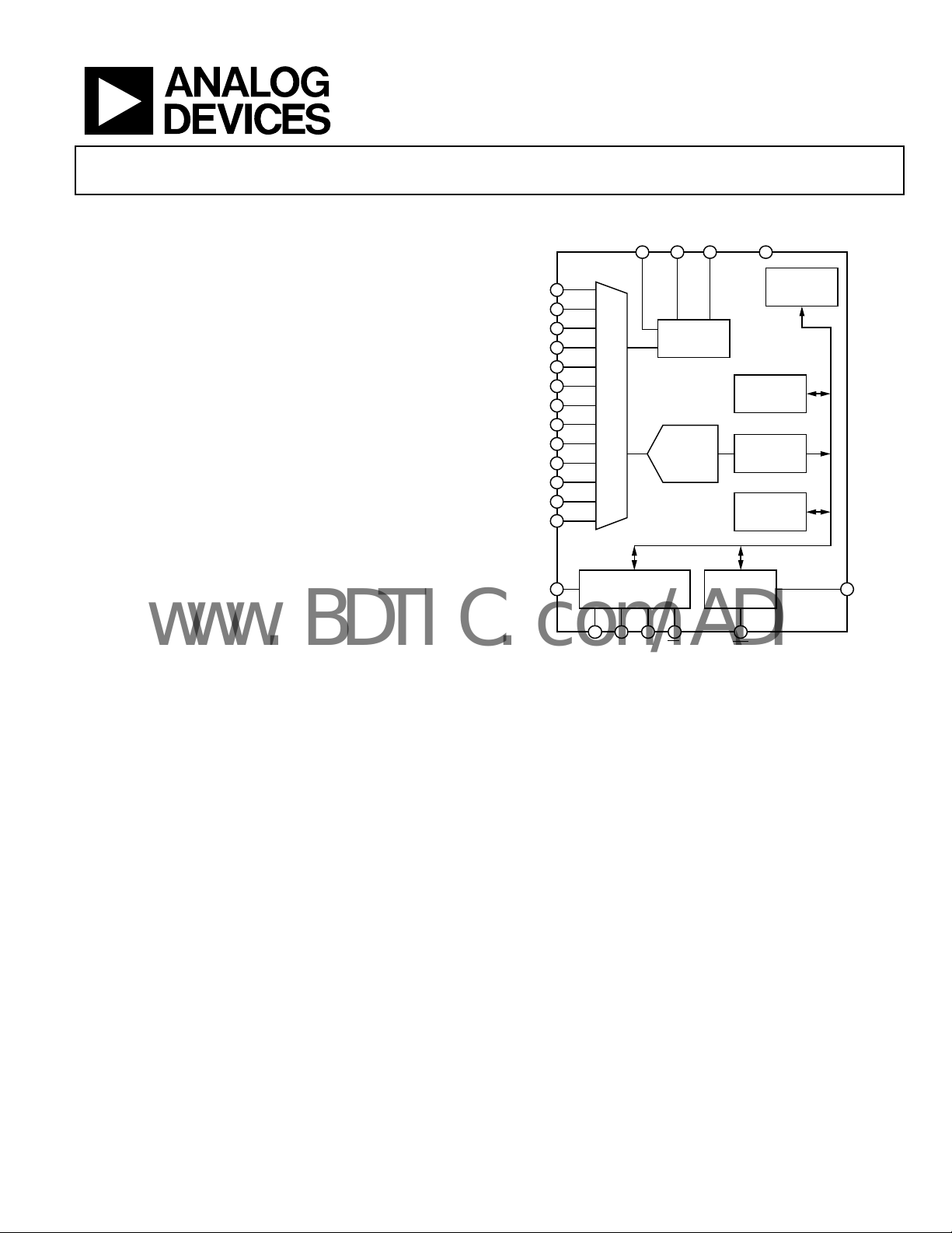
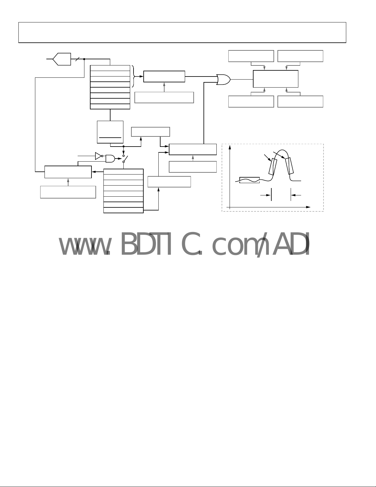
FUNCTIONAL BLOCK DIAGRAM
C
SHIELDVCC
8 11 10 9
19
CIN0
20
CIN1
21
CIN2
22
CIN3
23
CIN4
24
CIN5
1
CIN6
CIN7
CIN8
CIN9
CIN10
CIN11
CIN12
DRIVE
2
3
4
5
6
7
MATRIX
SWITCH
SERIAL INTERFACE
AND CONTROL LOGI C
13 14 15 16 17
SDO/
SDI/
ADD0
SCLK CS/
SDA
The AD7147 is designed for single electrode capacitance
sensors (grounded sensors). There is an active shield output to
minimize noise pickup in the sensor.
The AD7147 has on-chip calibration logic to compensate for
changes in the ambient environment. The calibration sequence
is performed automatically and at continuous intervals as long
as the sensors are not touched. This ensures that there are no
false or nonregistering touches on the external sensors due to
a changing environment.
The AD7147 has an SPI-compatible serial interface, and the
AD7147-1 has an I
2
C®-compatible serial interface. Both parts have
an interrupt output, as well as a GPIO. There is a V
the voltage level for the serial interface independent of V
The AD7147 is available in a 24-lead, 4 mm × 4 mm LFCSP and
operates from a 2.6 V to 3.6 V supply. The operating current consumption in low power mode is typically 26 A for 13 sensors.
EXCITATION
SOURCE
AD7147/
AD7147-1
16-BIT
-
CDC
ADD1
Figure 1.
GND BIAS
CALIBRATI ON
RAM
CALIBRATI ON
ENGINE
CONTROL
AND DATA
REGISTERS
INTERRUPT
AND GPIO
LOGIC
INT
POWER-ON
RESET LOGIC
DRIVE
1812
GPIO
pin to set
.
CC
06663-001
Rev. A
Information furnished by Analog Devices is believed to be accurate and reliable. However, no
responsibility is assumed by Analog Devices for its use, nor for any infringements of patents or other
rights of third parties that may result from its use. Specifications subject to change without notice. No
license is granted by implication or otherwise under any patent or patent rights of Analog Devices.
Trademarks and registered trademarks are the property of their respective owners.
One Technology Way, P.O. Box 9106, Norwood, MA 02062-9106, U.S.A.
Tel: 781.329.4700 www.analog.com
Fax: 781.461.3113 ©2007–2008 Analog Devices, Inc. All rights reserved.
Page 2

AD7147
www.BDTIC.com/ADI
TABLE OF CONTENTS
Features .............................................................................................. 1
Applications ....................................................................................... 1
General Description ......................................................................... 1
Functional Block Diagram .............................................................. 1
Revision History ............................................................................... 2
Specifications ..................................................................................... 3
Average Current Specifications .................................................. 4
SPI Timing Specifications (AD7147) ......................................... 5
I2C Timing Specifications (AD7147-1) ..................................... 6
Absolute Maximum Ratings ............................................................ 7
ESD Caution .................................................................................. 7
Pin Configurations and Function Descriptions ........................... 8
Typical Performance Characteristics ............................................. 9
Theory of Operation ...................................................................... 11
Capacitance Sensing Theory ..................................................... 11
BIAS Pin ....................................................................................... 12
Operating Modes ........................................................................ 12
Capacitiance-to-Digital Converter ............................................... 14
Oversampling the CDC Output ............................................... 14
Capacitance Sensor Offset Control .......................................... 14
Conversion Sequencer ............................................................... 14
CDC Conversion Sequence Time ............................................ 16
CDC Conversion Results ........................................................... 16
Capacitance Sensor Input Configuration .................................... 17
CINx Input Multiplexer Setup .................................................. 17
Single-Ended Connections to the CDC .................................. 17
Noncontact Proximity Detection ................................................. 18
Recalibration ............................................................................... 18
Proximity Sensitivity .................................................................. 18
FF_SKIP_CNT ............................................................................ 21
Environmental Calibration ........................................................... 23
Capacitance Sensor Behavior Without Calibration ............... 23
Threshold Equations .................................................................. 24
Capacitance Sensor Behavior with Calibration ...................... 24
Slow FIFO .................................................................................... 24
SLOW_FILTER_UPDATE_LVL .............................................. 25
Adaptive Threshold and Sensitivity ............................................. 26
Interrupt Output ............................................................................. 28
CDC Conversion-Complete Interrupt .................................... 28
Sensor-Touch Interrupt ............................................................. 28
INT
GPIO
Outputs ............................................................................................ 32
AC
General-Purpose Input/Output (GPIO) ................................. 32
Using the GPIO to Turn On/Off an LED ................................ 32
Serial Interface ................................................................................ 33
SPI Interface ................................................................................ 33
I2C-Compatible Interface .......................................................... 35
V
DRIVE
PCB Design Guidelines ................................................................. 38
Capacitive Sensor Board Mechanical Specifications ............. 38
Chip Scale Packages ................................................................... 38
Power-Up Sequence ....................................................................... 39
Typical Application Circuits ......................................................... 40
Register Map ................................................................................... 41
Detailed Register Descriptions ..................................................... 42
Bank 1 Registers ......................................................................... 42
Bank 2 Registers ......................................................................... 52
Bank 3 Registers ......................................................................... 57
Outline Dimensions ....................................................................... 69
Ordering Guide .......................................................................... 69
Output Control ....................................................... 30
Output .......................................................................... 32
SHIELD
Input ................................................................................. 37
REVISION HISTORY
8/08—Rev. 0 to Rev. A
Changes to Table 3 ............................................................................ 4
Added Figure 3, Renumbered Sequentially .................................. 6
Changes to Low Power Mode Section ......................................... 13
Added Latency from Touch to Response Section ...................... 13
Added Low Latency from Touch to Response Section .............. 13
Changes to Figure 60 and Figure 61 ............................................. 40
Changes to Figure 62 ...................................................................... 41
Added Exposed Pad Notation to Outline Dimensions ............. 69
Rev. A | Page 2 of 72
9/07—Revision 0: Initial Version
Page 3
AD7147
www.BDTIC.com/ADI
SPECIFICATIONS
VCC = 2.6 V to 3.6 V, TA = −40oC to +85°C, unless otherwise noted.
Table 1.
Parameter Min Typ Max Unit Test Conditions/Comments
CAPACITANCE-TO-DIGITAL CONVERTER
Update Rate 8.73 9 9.27 ms 12 conversion stages, decimation = 64
17.46 18 18.54 ms 12 conversion stages, decimation = 128
34.9 36 37.1 ms 12 conversion stages, decimation = 256
Resolution 16 Bits
CINx Input Range ±8 pF
No Missing Codes 16 Bits
CINx Input Leakage 25 nA
Maximum Output Load 20 pF Capacitance load on CINx to ground
Total Unadjusted Error ±20 %
Output Noise (Peak-to-Peak) 12 Codes Decimation rate = 64
7 Codes Decimation rate = 128
3 Codes Decimation rate = 256
Output Noise (RMS) 1.1 Codes Decimation rate = 64
0.8 Codes Decimation rate = 128
0.5 Codes Decimation rate = 256
C
Offset Range 20 pF
STRAY
C
Offset Resolution 0.32 pF
STRAY
Low Power Mode Delay Accuracy 4 %
AC
SHIELD
Frequency 250 kHz
Output Voltage 0 VCC V Oscillating
Short-Circuit Source Current 10 mA
Short-Circuit Sink Current 10 mA
Maximum Output Load 150 pF Capacitance load on AC
LOGIC INPUTS (SDI, SCLK, CS, SDA, GPIO)
VIH Input High Voltage 0.7 × V
V
DRIVE
VIL Input Low Voltage 0.4 V
IIH Input High Current −1 μA VIN = V
IIL Input Low Current 1 μA VIN = GND
Hysteresis 150 mV
OPEN-DRAIN OUTPUTS (SCLK, SDA, INT)
VOL Output Low Voltage 0.4 V I
IOH Output High Leakage Current ±0.1 ±1 μA V
LOGIC OUTPUTS (SDO, GPIO)
VOL Output Low Voltage 0.4 V I
VOH Output High Voltage V
GPIO, SDO Floating State Leakage
− 0.6 V I
DRIVE
±1 μA
Current
POWER
VCC 2.6 3.3 3.6 V
V
1.65 3.6 V Serial interface operating voltage
DRIVE
ICC 0.9 1 mA In full power mode, VCC + V
15.5 21.5 μA
2.3 7.5 μA Full shutdown, VCC + V
Rev. A | Page 3 of 72
Guaranteed by design, but not production
tested
Percentage of 200 ms, 400 ms, 600 ms,
or 800 ms
to ground
SHIELD
DRIVE
= −1 mA
SINK
= V
OUT
= 1 mA, V
SINK
SOURCE
DRIVE
DRIVE
= 1 mA, V
= 1.65 V to 3.6 V
= 1.65 V to 3.6 V
DRIVE
Pin three-state, leakage measured to
GND and V
Low power mode, converter idle, V
CC
DRIVE
+ V
CC
DRIVE,
decimation = 256
DRIVE
Page 4
AD7147
www.BDTIC.com/ADI
AVERAGE CURRENT SPECIFICATIONS
Table 2. Typical Average Current in Low Power Mode1
Low Power Decimation Current Values of Conversion Stages (A)
Mode Delay Rate 1 2 3 4 5 6 7 8 9 10 11 12
200 ms 64 20.83 24.18 27.52 30.82 34.11 37.37 40.6 43.81 46.99 50.16 53.3 56.41
128 25.3 31.92 38.45 44.87 51.21 57.45 63.6 69.66 75.63 81.52 87.33 93.05
256 34.11 46.99 59.51 71.66 83.47 94.94 106.1 116.96 127.52 137.81 147.82 157.58
400 ms 64 18.17 19.86 21.55 23.23 24.9 26.57 28.23 29.88 31.53 33.17 34.81 36.44
128 20.43 23.79 27.12 30.43 33.72 36.98 40.22 43.43 46.62 49.78 52.93 56.05
256 24.9 31.53 38.06 44.5 50.83 57.08 63.23 69.3 75.28 81.17 86.98 92.71
600 ms 64 17.28 18.41 19.54 20.67 21.79 22.91 24.03 25.14 26.25 27.36 28.47 29.57
128 18.79 21.04 23.28 25.51 27.73 29.94 32.13 34.32 36.49 38.65 40.81 42.95
256 21.79 26.25 30.67 35.04 39.37 43.66 47.9 52.11 56.27 60.39 64.47 68.51
800 ms 64 16.84 17.69 18.53 19.38 20.23 21.07 21.91 22.75 23.59 24.43 25.26 26.09
128 17.97 19.66 21.35 23.03 24.7 26.37 28.03 29.69 31.34 32.98 34.62 36.25
256 20.23 23.59 26.93 30.24 33.53 36.79 40.03 43.24 46.43 49.6 52.74 55.86
1
VCC = 3.3 V, TA = 25°C, load = 50 pF.
1
Table 3. Maximum Average Current in Low Power Mode
Low Power Decimation Current Values of Conversion Stages (A)
Mode Delay Rate 1 2 3 4 5 6 7 8 9 10 11 12
200 ms 64 27.96 32.06 36.12 40.15 44.16 48.12 52.06 55.97 59.85 63.69 67.51 71.29
128 33.41 41.49 49.44 57.26 64.97 72.55 80.02 87.37 94.61 101.74 108.77 115.69
256 44.16 59.85 75.05 89.79 104.09 117.97 131.45 144.53 157.25 169.61 181.63 193.33
400 ms 64 24.74 26.8 28.86 30.91 32.95 34.99 37.01 39.03 41.04 43.04 45.03 47.02
128 27.49 31.59 35.66 39.7 43.71 47.68 51.62 55.53 59.41 63.26 67.08 70.87
256 32.95 41.04 49 56.83 64.54 72.12 79.6 86.96 94.2 101.34 108.37 115.3
600 ms 64 23.66 25.04 26.42 27.79 29.17 30.53 31.89 33.25 34.61 35.96 37.31 38.66
128 25.5 28.25 30.99 33.71 36.41 39.1 41.78 44.44 47.09 49.72 52.34 54.95
256 29.17 34.61 40 45.33 50.6 55.82 60.98 66.09 71.15 76.15 81.1 86.01
800 ms 64 23.12 24.16 25.19 26.23 27.26 28.29 29.32 30.34 31.36 32.38 33.4 34.42
128 24.5 26.57 28.63 30.68 32.72 34.76 36.79 38.8 40.81 42.81 44.81 46.79
256 27.26 31.36 35.44 39.47 43.48 47.46 51.4 55.31 59.19 63.04 66.86 70.66
1
VCC = 3.6 V, TA = −40°C to +85°C, load = 50 pF.
Rev. A | Page 4 of 72
Page 5
AD7147
K
www.BDTIC.com/ADI
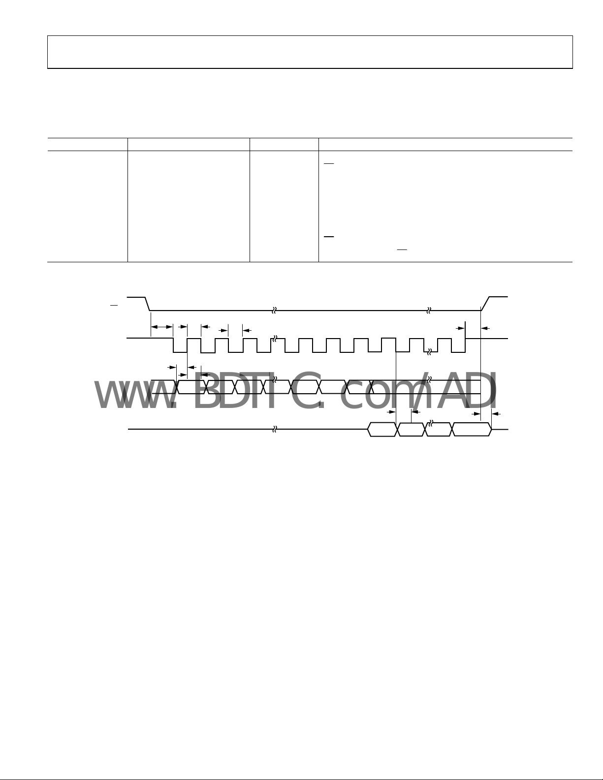
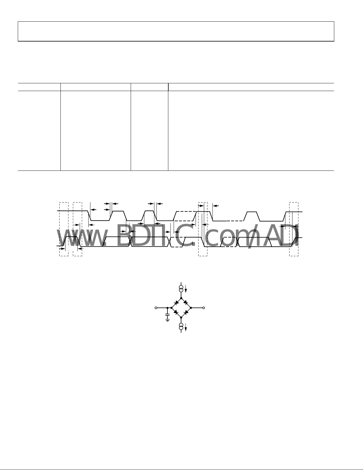
SPI TIMING SPECIFICATIONS (AD7147)
TA = −40°C to +85°C, sample tested at 25°C to ensure compliance. V
noted. All input signals are specified with t
= tF = 5 ns (10% to 90% of VCC) and timed from a voltage level of 1.6 V.
R
Table 4. SPI Timing Specifications
Parameter Limit Unit Description
f
5 MHz max SCLK frequency
SCLK
t1 5 ns min
t2 20 ns min SCLK high pulse width
t3 20 ns min SCLK low pulse width
t4 15 ns min SDI setup time
t5 15 ns min SDI hold time
t6 20 ns max SDO access time after SCLK falling edge
t7 16 ns max
t8 15 ns min
SPI Timing Diagram
CS
t
1
t
SCL
SDI
2
116
t
4
t
5
MSB LSB
t
3
23
= 1.65 V to 3.6 V, and VCC = 2.6 V to 3.6 V, unless otherwise
DRIVE
falling edge to first SCLK falling edge
CS
rising edge to SDO high impedance
CS
SCLK rising edge to CS
15
high
12
t
8
15
16
t
SDO
6
MSB
Figure 2. SPI Detailed Timing Diagram
LSB
t
7
06663-002
Rev. A | Page 5 of 72
Page 6
AD7147
www.BDTIC.com/ADI
I2C TIMING SPECIFICATIONS (AD7147-1)
TA = −40°C to +85°C, sample tested at 25°C to ensure compliance. V
noted. All input signals timed from a voltage level of 1.6 V.
Table 5. I
2
C Timing Specifications1
Parameter Limit Unit Description
f
400 kHz max
SCLK
t1 0.6 μs min Start condition hold time, t
t2 1.3 μs min Clock low period, t
t3 0.6 μs min Clock high period, t
t4 100 ns min Data setup time, t
t5 300 ns min Data hold time, t
t6 0.6 μs min Stop condition setup time, t
t7 0.6 μs min Start condition setup time, t
t8 1.3 μs min Bus-free time between stop and start conditions, t
tR 300 ns max Clock/data rise time
tF 300 ns max Clock/data fall time
1
Guaranteed by design, not production tested.
I2C Timing Diagram
t
t
2
SCLK
t
1
SDA
t
8
STOP START STOPSTART
R
t
5
t
F
t
3
Figure 3. I
t
4
2
C Detailed Timing Diagram
= 1.65 V to 3.6 V, and VCC = 2.6 V to 3.6 V, unless otherwise
DRIVE
HD; STA
LOW
HIGH
SU; DAT
HD; DAT
SU; STO
SU; STA
BUF
t
1
t
7
t
6
06663-003
TO OUTPUT
PIN
C
50pF
200µA I
L
200µA I
OL
1.6V
OH
06663-004
Figure 4. Load Circuit for Digital Output Timing Specifications
Rev. A | Page 6 of 72
Page 7
AD7147
www.BDTIC.com/ADI
ABSOLUTE MAXIMUM RATINGS
Table 6.
Parameter Rating
VCC to GND −0.3 V to +3.6 V
Analog Input Voltage to GND −0.3 V to VCC + 0.3 V
Digital Input Voltage to GND −0.3 V to V
Digital Output Voltage to GND −0.3 V to V
Input Current to Any Pin Except Supplies1 10 mA
ESD Rating (Human Body Model) 2.5 kV
Operating Temperature Range −40°C to +105°C
Storage Temperature Range −65°C to +150°C
Junction Temperature 150°C
LFCSP
Power Dissipation 450 mW
θJA Thermal Impedance 135.7°C/W
IR Reflow Peak Temperature 260°C (±0.5°C)
Lead Temperature (Soldering 10 sec) 300°C
1
Transient currents of up to 100 mA do not cause SCR latch-up.
DRIVE
DRIVE
+ 0.3 V
+ 0.3 V
Stresses above those listed under Absolute Maximum Ratings
may cause permanent damage to the device. This is a stress
rating only; functional operation of the device at these or any
other conditions above those indicated in the operational
section of this specification is not implied. Exposure to absolute
maximum rating conditions for extended periods may affect
device reliability.
ESD CAUTION
Rev. A | Page 7 of 72
Page 8
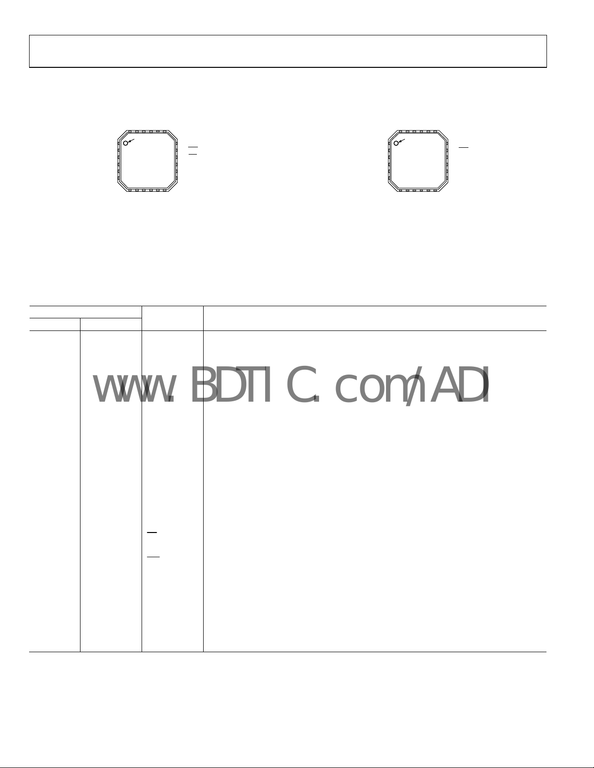
AD7147
www.BDTIC.com/ADI
PIN CONFIGURATIONS AND FUNCTION DESCRIPTIONS
CIN2
CIN3
CIN4
CIN5
CIN1
1CIN6
2CIN7
3CIN8
4CIN9
5CIN10
6CIN11
21
22
23
24
PIN 1
INDICAT OR
AD7147
TOP VIEW
(Not to Scale)
CIN0
20
19
18 GPIO
17 INT
16 CS
15 SCLK
14 SDI
13 SDO
1CIN6
2CIN7
3CIN8
4CIN9
5CIN10
6CIN11
CIN2
CIN3
CIN4
CIN5
21
22
23
24
PIN 1
INDICATO R
AD7147-1
TOP VIEW
(Not to Scale)
CIN1
CIN0
20
19
18 GPIO
17 INT
16 ADD1
15 SCLK
14 ADD0
13 SDA
9
7
8
12
10
11
CC
V
GND
BIAS
CIN12
NOTES
1. THE EXPOSED PAD IS NOT CONNECTED INT ERNALLY. FOR INCREASE D
RELIABILI TY OF THE SOLDER JOINTS AND MAXIMUM THERMAL CAPABILIT Y
IT IS RECO MMENDED THAT T HE PAD BE SOLDERED TO THE G ROUND PLANE.
AC
DRIVE
SHIELD
V
06663-005
NOTES
1. THE EXPOSED PAD IS NOT CONNECTED INT ERNALLY. FOR INCREASED
RELIABILI TY OF THE SOLDER JOINTS AND MAXI MUM THERMAL CAPABILITY
IT IS RECO MMENDED THAT T HE PAD BE SOLDERED TO THE G ROUND PLANE.
Figure 5. AD7147 Pin Configuration
Table 7. Pin Function Descriptions
Pin No.
AD7147 AD7147-1 Mnemonic Description
1 1 CIN6 Capacitance Sensor Input.
2 2 CIN7 Capacitance Sensor Input.
3 3 CIN8
4 4 CIN9
5 5 CIN10
6 6 CIN11
7 7 CIN12
8 8 AC
CDC Active Shield Output. Connect to external shield or plane.
SHIELD
9 9 BIAS
10 10 GND
11 11 V
12 12 V
Supply Voltage.
CC
Serial Interface Operating Voltage Supply.
DRIVE
13 N/A SDO
N/A 13 SDA
14 N/A SDI
N/A 14 ADD0
15 15 SCLK
16 N/A
CS
N/A 16 ADD1
17 17
INT
Capacitance Sensor Input.
Capacitance Sensor Input.
Capacitance Sensor Input.
Capacitance Sensor Input.
Capacitance Sensor Input.
Bias Node for Internal Circuitry. Requires 10 nF capacitor to ground.
Ground Reference Point for All Circuitry.
SPI Serial Data Output.
I2C Serial Data Input/Output. SDA requires pull-up resistor.
SPI Serial Data Input.
I2C Address Bit 0.
Clock Input for Serial Interface.
SPI Chip Select Signal.
I2C Address Bit 1.
General-Purpose Open-Drain Interrupt Output. Programmable polarity; requires pull-up resistor.
18 18 GPIO Programmable GPIO.
19 19 CIN0
20 20 CIN1
21 21 CIN2
22 22 CIN3
23 23 CIN4
Capacitance Sensor Input.
Capacitance Sensor Input.
Capacitance Sensor Input.
Capacitance Sensor Input.
Capacitance Sensor Input.
24 24 CIN5 Capacitance Sensor Input.
9
7
8
12
10
11
CC
V
GND
BIAS
CIN12
AC
DRIVE
SHIELD
V
Figure 6. AD7147-1 Pin Configuration
06663-006
Rev. A | Page 8 of 72
Page 9
AD7147
www.BDTIC.com/ADI
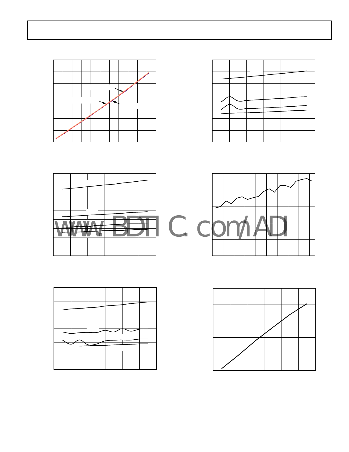
TYPICAL PERFORMANCE CHARACTERISTICS
935
70
915
895
875
(µA)
CC
I
855
835
815
795
DECIMATIO N = 128
2.6 3.7
2.7 2.8 2. 9 3.0 3. 1 3.2 3. 3 3.4 3. 5 3.6
DECIMATIO N = 64
DECIMATIO N = 256
VCC (V)
Figure 7. Supply Current vs. Supply Voltage
180
160
140
120
100
(A)
CC
80
I
60
40
20
0
2.5 3.7
2.7 2.9 3.1 3.3 3.5
200ms
400ms
600ms
800ms
VCC (V)
Figure 8. Low Power Supply Current vs. Supply Voltage,
Decimation Rate = 256
0.12
60
50
40
(A)
CC
I
30
20
10
06663-007
0
2.5 3.72.7 2.9 3.1 3. 3 3.5
200ms
400ms
600ms
800ms
06663-060
VCC (V)
Figure 10. Low Power Supply Current vs. Supply Voltage,
Decimation Rate = 64
2.5
2.0
1.5
(µA)
CC
I
1.0
0.5
06663-061
0
2.7
2.8 2.9 3.0 3.1 3.2 3.3 3.4 3.5 3.6
VCC (V)
06663-010
Figure 11. Shutdown Supply Current vs. Supply Voltage
1150
0.10
0.08
0.06
(mA)
CC
I
0.04
0.02
0
2.5 3.7
2.72.93.13.33.5
Figure 9. Low Power Supply Current vs. Supply Voltage,
200ms
400ms
VCC (V)
Decimation Rate = 128
600ms
800ms
1100
1050
(µA)
CC
I
1000
950
06663-009
900
0
100 200 300 400 500
AC
Figure 12. Supply Current vs. Capacitive Load on AC
Rev. A | Page 9 of 72
CAPACITIVE LOAD (pF)
SHIELD
SHIELD
06663-062
Page 10
AD7147
www.BDTIC.com/ADI
58000
56000
54000
52000
50000
48000
CDC CODE (d)
46000
44000
42000
40000
0
100 200 300 400 500
AC
CAPACITIVE LOAD (pF)
SHIELD
Figure 13. Output Code vs. Capacitive Load on AC
SHIELD
06663-063
160
140
120
100
CDC NOISE p-p (LSB)
25mV 75mV 125mV 175mV
50mV 100mV 150 mV 200mV
80
60
40
20
0
25
50
100
200
400
800
1600
3200
SINE WAVE FREQUENCY (Hz)
6400
12800
25600
51200
102400
Figure 16. Power Supply Sine Wave Rejection, VCC = 3.6 V
204800
409600
819200
06663-064
1640000
960
940
920
900
880
(µA)
CC
860
I
840
820
800
780
–60 –40 –20 0 20 40 60 80 100 120
3.6V
3.3V
2.6V
TEMPERATURE (° C)
Figure 14. Supply Current vs. Temperature
12
10
8
6
(µA)
CC
I
4
2
3.6V
3.3V
2.6V
120
100
CDC NOISE p-p (LSB)
06663-013
25mV 75mV 125mV 175mV
50mV 100mV 150 mV 200mV
80
60
40
20
0
25
50
100
200
400
800
1600
3200
SQUARE WAVE F REQUENCY (Hz)
6400
12800
25600
51200
102400
204800
409600
819200
06663-065
1640000
Figure 17. Power Supply Square Wave Rejection, VCC = 3.6 V
35
30
25
20
15
10
INPUT CAPACIT ANCE (pF)
5
0
–45 135
–25–51535557595115
TEMPERATURE (° C)
Figure 15. Shutdown Supply Current vs. Temperature
06663-014
0
0 10000 20000 30000 40000 50000 60000
CDC OUTPUT CODE
Figure 18. CDC Linearity, VCC = 3.3 V
Rev. A | Page 10 of 72
06663-016
Page 11
AD7147
www.BDTIC.com/ADI
THEORY OF OPERATION
The AD7147 and AD7147-1 are CDCs with on-chip environmental compensation. They are intended for use in portable
systems requiring high resolution user input. The internal
circuitry consists of a 16-bit, ∑-∆ converter that can change a
capacitive input signal into a digital value. There are 13 input
pins, CIN0 to CIN12, on the AD7147 or AD7147-1. A switch
matrix routes the input signals to the CDC. The result of each
capacitance-to-digital conversion is stored in on-chip registers.
The host subsequently reads the results over the serial interface.
The AD7147 has an SPI interface, and the AD7147-1 has an I
interface, ensuring that the parts are compatible with a wide
range of host processors. AD7147 refers to both the AD7147
and AD7147-1, unless otherwise noted, from this point forward
in this data sheet.
The AD7147 interfaces with up to 13 external capacitance
sensors. These sensors can be arranged as buttons, scroll bars,
or wheels, or as a combination of sensor types. The external
sensors consist of an electrode on a single- or multiple-layer
PCB that interfaces directly to the AD7147.
The AD7147 can be set up to implement any set of input
sensors by programming the on-chip registers. The registers
can also be programmed to control features such as averaging,
offsets, and gains for each of the external sensors. There is an
on-chip sequencer that controls how each of the capacitance
inputs is polled.
The AD7147 has on-chip digital logic and 528 words of RAM
that are used for environmental compensation. The effects of
humidity, temperature, and other environmental factors can
affect the operation of capacitance sensors. Transparent to the
user, the AD7147 performs continuous calibration to compensate for these effects, allowing the AD7147 to consistently
provide error-free results.
The AD7147 requires a companion algorithm that runs on the
host or another microcontroller to implement high resolution
sensor functions, such as scroll bars or wheels. However, no
companion algorithm is required to implement buttons. Button
sensors are implemented on chip, entirely in digital logic.
The AD7147 can be programmed to operate in either full power
mode or low power automatic wake-up mode. The automatic
wake-up mode is particularly suited for portable devices that
2
C
require low power operation to provide the user with significant
power savings and full functionality.
The AD7147 has an interrupt output,
new data has been placed into the registers.
interrupt the host on sensor activation. The AD7147 operates
from a 2.6 V to 3.6 V supply and is available in a 24-lead, 4 mm ×
4 mm LFCSP.
INT
, to indicate when
INT
is used to
CAPACITANCE SENSING THEORY
The AD7147 measures capacitance changes from single electrode
sensors. The sensor electrode on the PCB comprises one plate
of a virtual capacitor. The other plate of the capacitor is the user’s
finger, which is grounded with respect to the sensor input.
The AD7147 first outputs an excitation signal to charge the
plate of the capacitor. When the user comes close to the sensor,
the virtual capacitor is formed, with the user acting as the second
capacitor plate.
PLASTIC CO VER
SENSOR PCB
-
ADC
MUX
AD7147
Figure 19. Capacitance-Sensing Method
A square wave excitation signal is applied to CINx during
the conversion, and the modulator continuously samples the
charge going through CINx. The output of the modulator is
processed via a digital filter, and the resulting digital data is
stored in the CDC_RESULT_Sx registers for each conversion
stage, at Address 0x00B to Address 0x016.
16-BIT
DATA
EXCITATION
SIGNAL
250kHz
06663-017
Rev. A | Page 11 of 72
Page 12
AD7147
www.BDTIC.com/ADI
Registering a Sensor Activation
When a user approaches a sensor, the total capacitance associated
with that sensor changes and is measured by the AD7147. If
the change causes a set threshold to be exceeded, the AD7147
interprets this as a sensor activation.
On-chip threshold limits are used to determine when a sensor
activation occurs. Figure 20 shows the change in CDC_RESULT_Sx
when a user activates a sensor. The sensor is deemed to be active
only when the value of CDC_RESULT_Sx is either greater than the
value of STAGEx_HIGH_THRESHOLD or less than the value
of STAGEx_LOW_THRESHOLD.
SENSOR ACTIVE (A)
STAGEx_HIGH_THRESHOLD
CDC_RESULT_Sx
AMBIENT OR
NO-TOUCH VALUE
CDC OUTPUT CO DES
SENSOR ACTIVE (B)
Figure 20. Sensor Activation Thresholds
STAGEx_LOW _THRESHOLD
In Figure 20, two sensor activations are shown. Sensor Active A
occurs when a sensor is connected to the positive input of the
converter. In this case, when a user activates the sensor, there is an
increase in CDC code, and the value of CDC_RESULT_Sx exceeds
that of STAGEx_HIGH_THRESHOLD. Sensor Active B occurs
when the sensor is connected to the negative input of the converter.
In this case, when a user activates the sensor, there is a decrease
in CDC code, and the value of CDC_RESULT_Sx becomes less
than the value of STAGEx_LOW_THRESHOLD.
For each conversion stage, the STAGEx_HIGH_THRESHOLD
and STAGEx_LOW_THRESHOLD registers are in Register
Bank 3. The values in these registers are updated automatically
by the AD7147 due to its environmental calibration and
adaptive threshold logic.
At power-up, the values in the STAGEx_HIGH_THRESHOLD
and STAGEx_LOW_THRESHOLD registers are the same as those
in the STAGEx_OFFSET_HIGH and STAGEx_OFFSET_LOW
registers in Bank 2. The user must program the STAGEx_OFFSET
_HIGH and STAGEx_OFFSET_LOW registers on device powerup. See the Environmental Calibration section of the data sheet
for more information.
06663-018
Complete Solution for Capacitance Sensing
Analog Devices, Inc., provides a complete solution for
capacitance sensing. The two main elements to the solution are
the sensor PCB and the AD7147.
If the application requires high resolution sensors such as scroll
bars or wheels, software is required that runs on the host
processor. The memory requirements for the host depend on
the sensor and are typically 10 kB of code and 600 bytes of data
memory, depending on the sensor type.
SENSOR PCB
AD7147
Figure 21. Three-Part Capacitance Sensing Solution
SPI OR I2C
HOST PROCESSOR
1 MIPS
10kB ROM
600 BYTES RAM
06663-019
Analog Devices supplies the sensor PCB footprint design
libraries to the customer and supplies any necessary software on
an open source basis.
BIAS PIN
This pin is connected internally to a bias node of the AD7147.
To ensure correct operation of the AD7147, connect a 10 nF
capacitor between the BIAS pin and ground. The voltage seen at
the BIAS pin is V
/2.
CC
OPERATING MODES
The AD7147 has three operating modes. Full power mode, where
the device is always fully powered, is suited for applications where
power is not a concern (for example, game consoles that have an
ac power supply). Low power mode, where the part automatically
powers down when no sensor is active, is tailored to provide
significant power savings compared with full power mode and
is suited for mobile applications, where power must be
conserved. In shutdown mode, the part shuts down completely.
The POWER_MODE bits (Bit 0 and Bit 1) of the control
register set the operating mode on the AD7147. The control
register is at Address 0x000. Ta ble 8 shows the POWER_MODE
settings for each operating mode. To put the AD7147 into
shutdown mode, set the POWER_MODE bits to either 01 or 11.
Table 8. POWER_MODE Settings
POWER_MODE Bits Operating Mode
00 Full power mode
01 Shutdown mode
10 Low power mode
11 Shutdown mode
The power-on default setting of the POWER_MODE bits is 00,
full power mode.
Rev. A | Page 12 of 72
Page 13
AD7147
www.BDTIC.com/ADI
Full Power Mode
In full power mode, all sections of the AD7147 remain fully
powered and converting at all times. While a sensor is being
touched, the AD7147 processes the sensor data. If no sensor is
touched, the AD7147 measures the ambient capacitance level
and uses this data for the on-chip compensation routines. In full
power mode, the AD7147 converts at a constant rate. See the
CDC Conversion Sequence Time section for more information.
Low Power Mode
When AD7147 is in low power mode, the POWER_MODE bits
are set to 10 upon device initialization. If the external sensors
are not touched, the AD7147 reduces its conversion frequency,
thereby greatly reducing its power consumption. The part remains
in a reduced power state while the sensors are not touched. The
AD7147 performs a conversion after a delay defined by the
LP_CONV_DELAY bits, and it uses this data to update the
compensation logic and check if the sensors are active. The
LP_CONV_DELAY bits set the delay between conversions to
200 ms, 400 ms, 600 ms, or 800 ms.
In low power mode, the total current consumption of the AD7147
is an average of the current used during a conversion and the
current used while the AD7147 is waiting for the next conversion
to begin. For example, when LP_CONV_DELAY is 400 ms, the
AD7147 typically uses 0.85 mA of current for 36 ms and 14 A
of current for 400 ms during the conversion interval. (Note that
these conversion timings can be altered through the register
AD7147 SETUP
AND INITIAL IZATIO N
POWER_MO DE = 10
settings. See the CDC Conversion Sequence Time section for
more information.)
The time for the AD7147 to transition from a full power state to
a reduced power state after the user stops touching the external
sensors is configurable. The PWR_DOWN_TIMEOUT bits (in
the Ambient Compensation Control 0 (AMB_COMP_CTRL0)
Register at Address 0x002) control the time delay before the
AD7147 transitions to the reduced power state after the user
stops touching the sensors.
Latency from Touch to Response
In low power mode, the AD7147 remains in a low power state
until any one of the external sensors are touched. When a
sensor is touched, the AD7147 begins a conversion sequence
every 36 ms to read back data from the sensors. This means that
the latency between the user touching the sensor, and the AD7147
responding, is a maximum of LP_CONV_DELAY ms.
Low Latency from Touch to Response
In low power mode, the AD7147P model remains in a low power
state until proximity is detected on any one of the external sensors.
When proximity is detected, the AD714P begins a conversion
sequence every 36 ms, or 18 ms, or 9 ms to readback data from the
sensors. The latency between first touch and the AD7147P
responding is much reduced, compared to the AD7147, because
the part is already in a full power state by the time the user has
touched the sensor.
AD7147P SETUP
AND INITIAL IZATIO N
POWER_MODE = 10
CONVERSION S EQUENCE
EVERY LP_CONV_DELAY
UPDATE COMPENSAT ION
LOGIC DAT A PATH
Figure 22. Low Power Mode Operation, AD7147
ANY
NO YES
SENSOR
TOUCHED?
YES
CONVERSION SEQUENCE
EVERY 9/18/ 36ms FOR
SENSOR READBACK
ANY SENSOR
TOUCHED?
NO
PROXIMITY TIMER
COUNTDOWN
TIMEOUT
Rev. A | Page 13 of 72
USER IN
NO YES
PROXIMITY
TO SENSOR?
CONVERSION SEQUENCE
EVERY LP_CONV_DELAY
UPDATE COMPENSAT ION
LOGI C DATA PAT H
06663-020
Figure 23. Low Power Mode Operation, AD7147P
CONVERSION SEQUENCE
EVERY 9/18/ 36ms FOR
SENSOR READBACK
USER IN
YES
PROXIMITY
TO SENSOR?
NO
PROXIMITY TIMER
COUNTDO WN
TIMEOUT
06663-066
Page 14
AD7147
www.BDTIC.com/ADI
CAPACITIANCE-TO-DIGITAL CONVERTER
The capacitance-to-digital converter on the AD7147 has a Σ-
architecture with 16-bit resolution. There are 13 possible inputs to
the CDC that are connected to the input of the converter through a
switch matrix. The sampling frequency of the CDC is 250 kHz.
OVERSAMPLING THE CDC OUTPUT
The decimation rate, or oversampling ratio, is determined by
Bits[9:8] of the power control (PWR_CONTROL) register
(Address 0x000), as listed in Tab le 9 .
from midscale, decrease the POS_AFE_OFFSET or
NEG_AFE_OFFSET value by 1.
The goal is to ensure that the CDC_RESULT_Sx is as close
to midscale as possible. This process is only required once
during the initial capacitance sensor characterization.
+DAC
(20pF RANGE)
6
POS_AFE_OFFSET
Table 9. CDC Decimation Rate
CDC Output Rate
Decimation Bits Decimation Rate
00 256 3.072
01 128 1.536
10 64 0.768
11 64 0.768
Per Stage (ms)
The decimation process on the AD7147 is an averaging process,
where a number of samples are taken and the averaged result is
output. Due to the architecture of the digital filter employed, the
number of samples taken (per stage) is equal to 3× the decimation
rate. So 3 × 256 or 3 × 128 samples are averaged to obtain each
stage result.
The decimation process reduces the amount of noise present in
the final CDC result. However, the higher the decimation rate,
the lower the output rate per stage; therefore, there is a trade-off
possible between the amount of noise in the signal and the
speed of sampling.
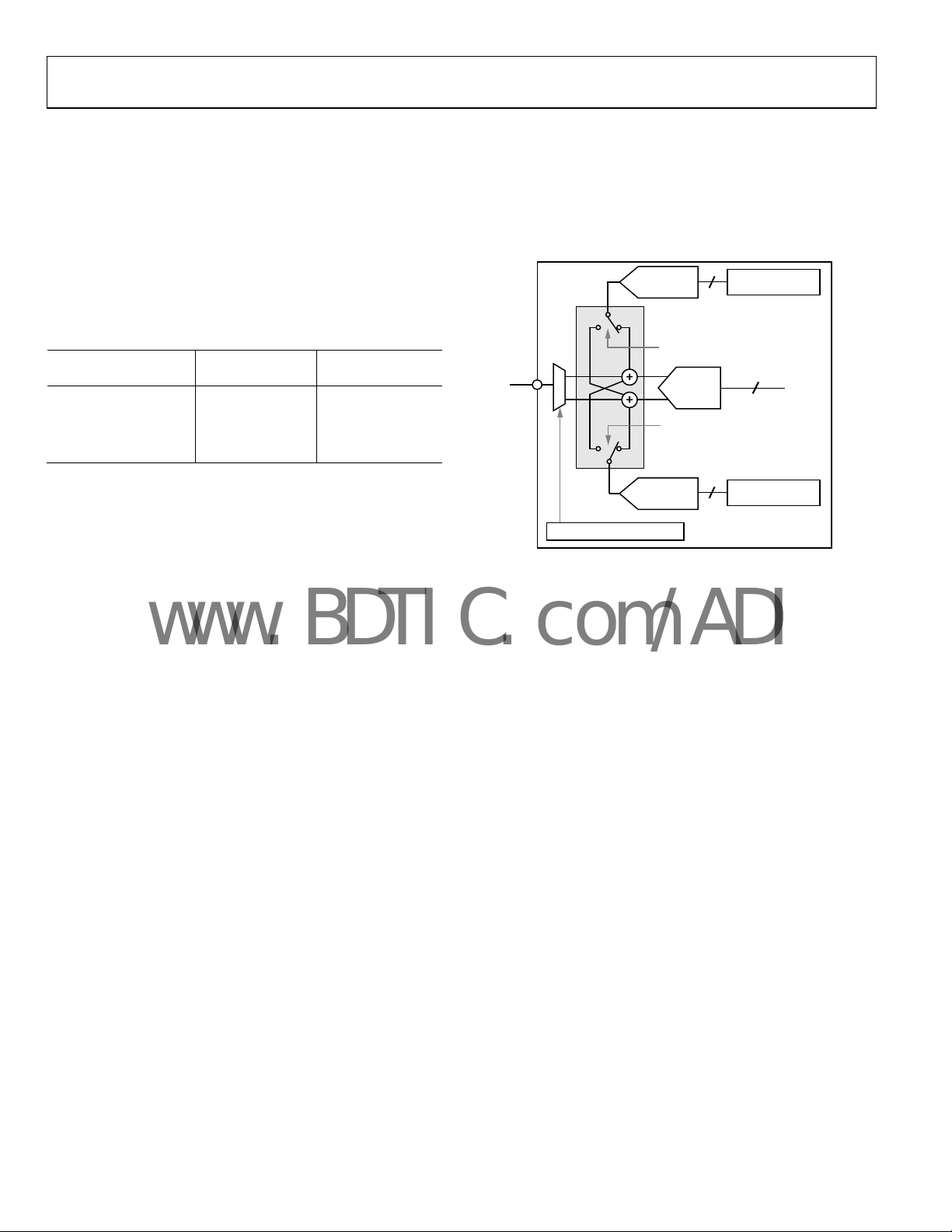
CAPACITANCE SENSOR OFFSET CONTROL
There are two programmable DACs on board the AD7147 to null
the effect of any stray capacitances on the CDC measurement.
These offsets are due to stray capacitance to ground.
A simplified block diagram in Figure 24 shows how to apply the
STAGEx_AFE_OFFSET registers to null the offsets. The 6-bit
POS_AFE_OFFSET and NEG_AFE_OFFSET bits program the
offset DAC to provide 0.32 pF resolution offset adjustment over
a range of 20 pF.
The best practice is to ensure that the CDC output for any stage
is approximately equal to midscale (~32,700) when all sensors
are inactive. To correctly offset the stray capacitance to ground for
each stage, use the following procedure:
1. Read back the CDC value from the CDC_RESULT_Sx register.
2. If this value is not close to midscale, increase the value of
POS_AFE_OFFSET or NEG_AFE_OFFSET (depending
on if the CINx input is connected to the positive or negative
input of the converter) by 1. The CINx connections are
determined by the STAGEx_CONNECTION registers.
3. If the CDC value in CDC_RESULT_Sx is now closer
to midscale, repeat Step 2. If the CDC value is further
POS_AFE_OFFSET_SWAP BIT
CINx
CINx_CONNECTION_SETUP
Figure 24. Analog Front-End Offset Control
+
16-BIT
CDC
_
NEG_AFE_OF FSET_SW AP BIT
–DAC
(20pF RANGE)
6
16
NEG_AFE_OFFSET
06663-021
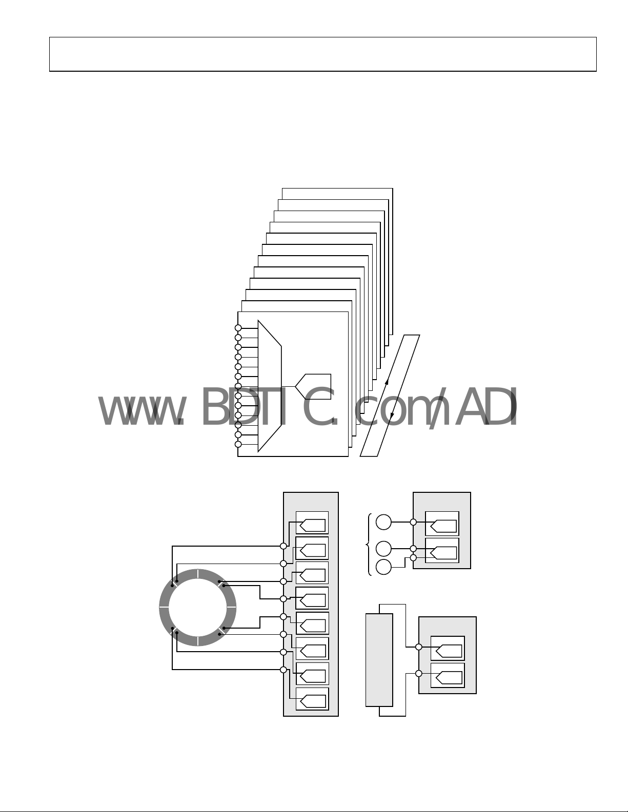
CONVERSION SEQUENCER
The AD7147 has an on-chip sequencer to implement conversion
control for the input channels. Up to 12 conversion stages can be
performed in one sequence. Each of the 12 conversions stages can
measure the input from a different sensor. By using the Bank 2
registers, each stage can be uniquely configured to support multiple
capacitance sensor interface requirements. For example, a slider
sensor can be assigned to STAGE1 through STAGE8, with a
button sensor assigned to STAGE0. For each conversion stage,
the input mux that connects the CINx inputs to the converter
can have a unique setting.
The AD7147 on-chip sequence controller provides conversion
control, beginning with STAGE0. Figure 25 shows a block diagram
of the CDC conversion stages and CINx inputs. A conversion
sequence is defined as a sequence of CDC conversions starting
at STAGE0 and ending at the stage determined by the value
programmed in the SEQUENCE_STAGE_NUM bits. Depending
on the number and type of capacitance sensors that are used, not all
conversion stages are required. Use the SEQUENCE_STAGE_NUM
bits to set the number of conversions in one sequence. This number
depends on the sensor interface requirements. For example, the
register should be set to 5 if the CINx inputs are mapped to only six
conversion stages. In addition, the STAGE_CAL_EN register
should be set according to the number of stages that are used.
The number of required conversion stages depends solely on
the number of sensors attached to the AD7147. Figure 26 shows
how many conversion stages are required for each sensor and
how many inputs to the AD7147 each sensor requires.
Rev. A | Page 14 of 72
Page 15
AD7147
www.BDTIC.com/ADI
A button sensor generally requires one sequencer stage; this is
shown in Figure 26 as B1. However, it is possible to configure
two button sensors to operate differentially for one conversion
stage. Only one button can be activated at a time; pressing both
buttons simultaneously results in neither button being activated.
The configuration with two button sensors operating differentially
requires one conversion stage and is shown in Figure 26, with
B2 and B3 representing the differentially configured button sensors.
STAGE4
STAGE3
STAGE2
STAGE1
STAGE0
CIN0
CIN1
CIN2
CIN3
CIN4
CIN5
CIN6
CIN7
CIN8
CIN9
CIN10
CIN11
CIN12
SWITCH MA TRIX
Figure 25. CDC Conversion Stages
STAGE7
STAGE6
STAGE5
16-BIT
ADC
A wheel sensor requires eight stages, whereas a slider requires two
stages. The result from each stage is used by the host software to
determine the user’s position on the slider or wheel. The algorithms
that perform this process are available from Analog Devices and are
free of charge, but require signing a software license.
STAGE11
STAGE10
STAGE9
STAGE8
E
C
N
E
-
U
Q
E
S
N
O
I
S
R
E
V
N
O
C
06663-022
SCROLL
WHEEL
AD7147
SEQUENCER
STAGE0
+
CDC
–
STAGE1
+
CDC
–
STAGE2
+
CDC
–
STAGE3
+
CDC
–
STAGE4
+
CDC
–
STAGE5
+
CDC
–
STAGE6
+
CDC
–
STAGE7
+
CDC
–
BUTTONS
B1
B2
B3
SLIDER
AD7147
SEQUENCER
STAGE8
+
CDC
–
STAGE9
+
CDC
–
AD7147
SEQUENCER
STAGE10
+
CDC
–
STAGE11
+
CDC
–
06663-023
Figure 26. Sequencer Setup for Sensors
Rev. A | Page 15 of 72
Page 16
AD7147
C
www.BDTIC.com/ADI
CDC CONVERSION SEQUENCE TIME
Table 10. CDC Conversion Times for Full Power Mode
Conversion Time (ms)
SEQUENCE_STAGE_NUM Decimation = 64 Decimation = 128 Decimation = 256
0 0.768 1.536 3.072
1 1.536 3.072 6.144
2 2.304 4.608 9.216
3 3.072 6.144 12.288
4 3.84 7.68 15.36
5 4.608 9.216 18.432
6 5.376 10.752 21.504
7 6.144 12.288 24.576
8 6.912 13.824 27.648
9 7.68 15.36 30.72
10 8.448 16.896 33.792
11 9.216 18.432 36.864
The time required for the CDC to complete the measurement of
all 12 stages is defined as the CDC conversion sequence time. The
SEQUENCE_STAGE_NUM and DECIMATION bits determine
the conversion time, as listed in Tab le 1 0.
For example, if the device is operated with a decimation rate
of 128 and the SEQUENCE_STAGE_NUM bit is set to 5 for the
conversion of six stages in a sequence, the conversion sequence
time is 9.216 ms.
Full Power Mode CDC Conversion Sequence Time
The full power mode CDC conversion sequence time for all
12 stages is set by configuring the SEQUENCE_STAGE_NUM
and DECIMATION bits as outlined in Tabl e 10 .
Figure 27 shows a simplified timing diagram of the full power
mode CDC conversion time. The full power mode CDC conversion time (t
CDC
ONVERSION
Figure 27. Full Power Mode CDC Conversion Sequence Time
) is set using the values shown in Tabl e 10 .
CONV_FP
t
CONV_FP
CONVERSION
SEQUENCE N
CONVERSION
SEQUENCE N + 1
CONVERSION
SEQUENCE N + 2
6663-024
Low Power Mode CDC Conversion Sequence Time with Delay
The frequency of each CDC conversion while operating in the
low power automatic wake-up mode is controlled by using the
LP_CONV_DELAY bits located at Address 0x000[3:2] in
addition to the registers listed in Tab le 1 0 . This feature provides
some flexibility for optimizing the tradeoff between the conversion
time needed to meet system requirements and the power
consumption of the AD7147.
For example, maximum power savings is achieved when the
LP_CONV_DELAY bits are set to 11. With a setting of 11,
the AD7147 automatically wakes up, performing a conversion
every 800 ms.
Table 11. LP_CONV_DELAY Settings
LP_CONV_DELAY Bits Delay Between Conversions (ms)
00 200
01 400
10 600
11 800
Figure 28 shows a simplified timing example of the low power
mode CDC conversion time. As shown, the low power mode CDC
conversion time is set by t
t
CONV_FP
CDC
CONVERSION
CONVERSION
SEQUENCE N
Figure 28. Low Power Mode CDC Conversion Sequence Time
and the LP_CONV_DELAY bits.
CONV_FP
t
CONV_LP
LP_CONV_DELAY
CONVERSION
SEQUENCE N + 1
6663-025
CDC CONVERSION RESULTS
Certain high resolution sensors require the host to read back the
CDC conversion results for processing. The registers required
for host processing are located in the Bank 3 registers. The host
processes the data read back from these registers using a software
algorithm in order to determine position information.
In addition to the results registers in the Bank 3 registers, the
AD7147 provides the 16-bit CDC output data directly, starting
at Address 0x00B of Bank 1. Reading back the CDC 16-bit
conversion data register allows for customer-specific application
data processing.
Rev. A | Page 16 of 72
Page 17

AD7147
www.BDTIC.com/ADI
CAPACITANCE SENSOR INPUT CONFIGURATION
Each input connection from the external capacitance sensors to
the converter of the AD7147 can be uniquely configured by
using the registers in Bank 2 (see Table 3 8). These registers are
used to configure the input pin connection setups, sensor offsets,
sensor sensitivities, and sensor limits for each stage. Each sensor
can be individually optimized. For example, a button sensor
connected to STAGE0 can have different sensitivity and offset
values than a button with another function that is connected to a
different stage.
CINx INPUT MULTIPLEXER SETUP
Tabl e 34 and Ta bl e 35 list the available options for the
CINx_CONNECTION_SETUP bits when the sensor input
pins are connected to the CDC.
The AD7147 has an on-chip multiplexer that routes the input
signals from each CINx pin to the input of the converter. Each
input pin can be tied to either the negative or positive input of
the CDC, or it can be left floating. Each input can also be
internally connected to the BIAS signal to help prevent cross
coupling. If an input is not used, always connect it to the BIAS.
Connecting a CINx input pin to the positive CDC input results
in an increase in CDC output code when the corresponding
sensor is activated. Connecting a CINx input pin to the negative
CDC input results in a decrease in CDC output code when the
corresponding sensor is activated.
The AD7147 performs a sequence of 12 conversions. The multiplexer can have different settings for each of the 12 conversions.
For example, CIN0 is connected to the negative CDC input for
conversion STAGE1, left floating for conversion STAGE1, and
so on, for all 12 conversion stages.
For each CINx input for each conversion stage, two bits control
how the input is connected to the converter, as shown in Figure 29.
Examples
To connect CIN3 to the positive CDC input on Stage 0 use the
following setting:
STAGE0_CONNECTION[6:0] = 0xFFBF
STAGE0_CONNECTION[12:7] = 0x2FFF
To connect CIN0 to the positive CDC input and CIN12 to the
negative CIN input on Stage 5 use the following settings:
STAGE5_CONNECTION[6:0] = 0xFFFE
STAGE5_CONNECTION[12:7] = 0x37FF
SINGLE-ENDED CONNECTIONS TO THE CDC
A single-ended connection to the CDC is defined as one CINx
input connected to either the positive or negative CDC input
for one conversion stage. A differential connection to the CDC is
defined as one CINx input connected to the positive CDC input
and a second CINx input connected to the negative input of the
CDC for one conversion stage.
For any stage, if a single-ended connection to the CDC is made
in that stage, the SE_CONNECTION_SETUP bits (Bits[13:12] in
the STAGEx_CONNECTION[12:7] register) should be applied as
follows:
• SE_CONNECTION_SETUP = 00: do not use.
• SE_CONNECTION_SETUP = 01: single-ended connection.
For this stage, there is one CINx connected to the positive
CDC input.
• SE_CONNECTION_SETUP = 10: single-ended connection.
For this stage, there is one CINx connected to the negative
CDC input.
• SE_CONNECTION_SETUP = 11: differential connection.
For this stage, there is one CINx connected to the nega
tive CDC input and one CINx connected to the positive
CDC input.
These bits ensure that during a single-ended connection to the
CDC, the input paths to both CDC terminals are matched,
which in turn improves the power-supply rejection of the
converter measurement.
These bits should be applied in addition to setting the other bits
in the STAGEx_CONNECTION registers, as outlined in the
CINx Input Multiplexer Setup section.
If more than one CINx input is connected to either the positive
or negative input of the converter for the same conversion, set
SE_CONNECTION_SETUP to 11. For example, if CIN0 and
CIN3 are connected to the positive input of the CDC, set
SE_CONNECTION_SETUP to 11.
CIN CONNECTION SETUP BITS CIN SETTING
CIN0
CIN1
CIN2
CIN3
CIN4
CIN5
CIN6
CIN7
CIN8
CIN9
CIN10
CIN11
CIN12
00 CI Nx FLOATING
01
10
11
Figure 29. Input Mux Configuration Options
CINx CONNECTED T O
NEGATIVE CDC INPUT
CINx CONNECTED T O
POSITIVE CDC INPUT
CINx CONNECTED T O
BIAS
Rev. A | Page 17 of 72
+
CDC
–
06663-026
Page 18

AD7147
www.BDTIC.com/ADI
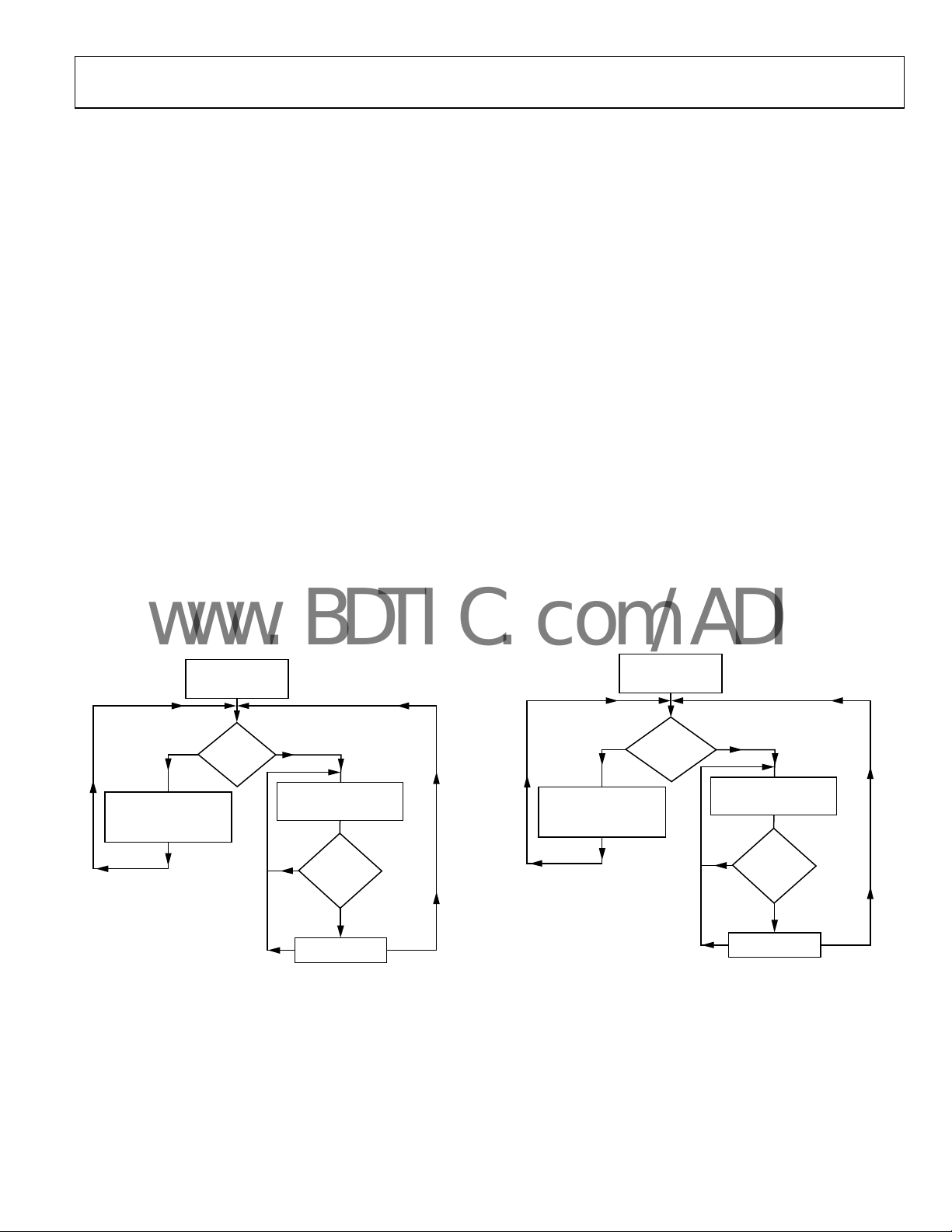
NONCONTACT PROXIMITY DETECTION
The AD7147 internal signal processing continuously monitors
all capacitance sensors for noncontact proximity detection. This
feature provides the ability to detect when a user is approaching
a sensor, at which time all internal calibration is immediately
disabled while the AD7147 is automatically configured to detect
a valid contact.
The proximity control register bits are described in Ta ble 1 2. The
FP_PROXIMITY_CNT and LP_PROXIMITY_CNT register
bits control the length of the calibration disable period after
the user stops touching the sensor and is not in close proximity
to the sensor during full or low power mode. The calibration is
disabled during this period and then enabled again. Figure 30
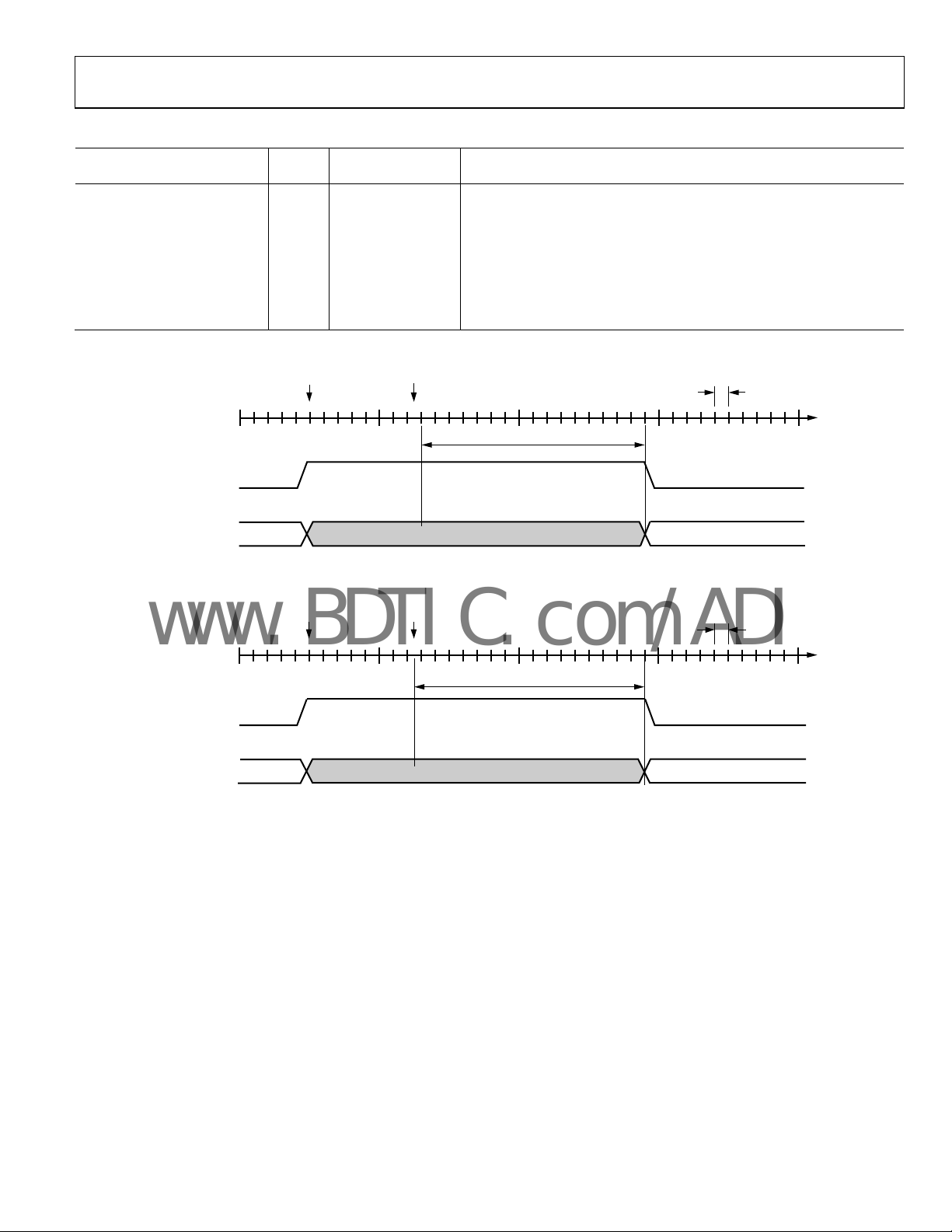
and Figure 31 show examples of how these registers are used to set
the calibration disable periods for the full and low power modes.
The calibration disable period in full power mode is the value
of the FP_PROXIMITY_CNT multiplied by 16 multiplied by
the time for one conversion sequence in full power mode. The
calibration disable period in low power mode is the value of the
LP_PROXIMITY_CNT multiplied by 4 multiplied by the time
for one conversion sequence in low power mode.
by the PROXIMITY_RECAL_LVL bits for a set period of time
known as the recalibration timeout. In full power mode, the recalibration timeout is controlled by FP_PROXIMITY_RECAL; in
low power mode, by LP_PROXMTY_RECAL.
The recalibration timeout in full power mode is the value of
the FP_PROXIMITY_RECAL multiplied by the time for one
conversion sequence in full power mode. The recalibration timeout in low power mode is the value of the LP_PROXIMITY_
RECAL multiplied by the time for one conversion sequence in
low power mode.
Figure 32 and Figure 33 show examples of how the
FP_PROXIMITY_RECAL and LP_PROXIMITY_RECAL
register bits control the timeout period before a recalibration
while operating in the full and low power modes. In these
examples, a user approaches a sensor and then leaves, but the
proximity detection remains active. The measured CDC value
exceeds the stored ambient value by the amount set in the
PROXIMITY_RECAL_LVL bits for the entire timeout period.
The sensor is automatically recalibrated at the end of the
timeout period.
RECALIBRATION
In certain situations (for example, when a user hovers over a
sensor for a long time), the proximity flag can be set for a long
period. The environmental calibration on the AD7147 is suspended while proximity is detected, but changes may occur
to the ambient capacitance level during the proximity event.
This means that the ambient value stored on the AD7147 no
longer represents the actual ambient value. In this case, even
when the user is not in close proximity to the sensor, the proximity flag may still be set. This situation can occur if the user
interaction creates some moisture on the sensor, causing the
new sensor ambient value to be different from the expected
value. In this situation, the AD7147 automatically forces a
recalibration internally. This ensures that the ambient values
are recalibrated, regardless of how long the user hovers over
the sensor. A recalibration ensures maximum AD7147 sensor
performance.
The AD7147 recalibrates automatically when the measured CDC
value exceeds the stored ambient value by an amount determined
PROXIMITY SENSITIVITY
The fast filter in Figure 34 is used to detect when someone is close
to the sensor (proximity). Two conditions, detected by Comparator 1 and Comparator 2, set the internal proximity detection
signal: Comparator 1 detects when a user is approaching or
leaving a sensor, and Comparator 2 detects when a user hovers
over a sensor or approaches a sensor very slowly.
The sensitivity of Comparator 1 is controlled by the
PROXIMITY_DETECTION_RATE bits. For example, if
PROXIMITY_DETECTION_RATE is set to 4, the Proximity 1
signal is set when the absolute difference between WORD1 and
WORD3 exceeds (4 × 16) LSB codes.
The PROXIMITY_RECAL_LVL bits (Address 0x003) control
the sensitivity of Comparator 2. For example, if PROXIMITY_
RECAL_LVL is set to 75, the Proximity 2 signal is set when the
absolute difference between the fast filter average value and the
ambient value exceeds (75 × 16) LSB codes.
Rev. A | Page 18 of 72
Page 19
AD7147
www.BDTIC.com/ADI
Table 12. Proximity Control Registers (See Figure 34)
Length
Bit Name
FP_PROXIMITY_CNT 4 0x002[7:4] Calibration disable time in full power mode.
LP_PROXIMITY_CNT 4 0x002[11:8] Calibration disable time in low power mode.
FP_PROXIMITY_RECAL 8 0x004[9:0] Full power mode proximity recalibration time.
LP_PROXIMITY_RECAL 6 0x004[15:10] Low power mode proximity recalibration time.
PROXIMITY_RECAL_LVL 8 0x003[7:0]
PROXIMITY_DETECTION_RATE 6 0x003[13:8]
CDC CONVERSION
SEQUENCE
(INTERNAL)
PROXIMITY
DETECTIO N
(INTERNAL)
(Bits) Register Address Description
Proximity recalibration level. This value multiplied by 16 controls the
sensitivity of Comparator 2 (see Figure 34).
Proximity detection rate. This value multiplied by 16 controls the
sensitivity of Comparator 1 (see Figure 34).
USER APPROACHES
SENSOR
12345678910111213141516
USER LEAVES
SENSOR AREA
t
CALDIS
17 18 19 20 21 22 23 24
t
CONV_FP
CALIBRATIO N
(INTERNAL)
CALIBRATION ENABLEDCALIBRATION DISABLED
06663-027
Figure 30. Example of Full Power Mode Proximity Detection (FP_PROXIMITY_CNT = 1)
USER LEAVES
SENSOR AREA
t
=
CONV_LP
t
CONV_FP
17 18 19 20 21 22 23 24
t
CALDIS
+ LP_CONV_DELAY.
t
CONV_LP
CALIBRATION ENABLEDCALIBRATION DISABL ED
06663-028
CDC CONVERSION
SEQUENCE
(INTERNAL)
PROXIMITY
DETECTIO N
(INTERNAL)
CALIBRATIO N
(INTERNAL)
USER APPROACHES
SENSOR
12345678910111213141516
NOTES
1. SEQUENCE CO NVERSION T IME
2. PROXIMITY IS SET WHEN USER APPROACHES THE SENS OR, AT WHI CH TIME T HE INTERNAL CAL IBRATION I S DISABLED.
3.
t
= (
t
CALDIS
× LP_PROXI MITY_CNT × 4).
CONV_LP
Figure 31. Example of Low Power Mode Proximity Detection (LP_PROXIMITY_CNT = 4)
Rev. A | Page 19 of 72
Page 20

AD7147
www.BDTIC.com/ADI
CDC CONVERSION
SEQUENCE
(INTERNAL)
PROXIMITY
DETECTIO N
(INTERNAL)
CALIBRATIO N
(INTERNAL)
RECALIBRATIO N
COUNTER
(INTERNAL)
Figure 32. Example of Full Power Mode Proximity Detection with Forced Recalibration (FP_PROXIMITY_CNT = 1 and FP_PROXIMITY_RECAL = 40)
CDC CONVERSION
SEQUENCE
(INTERNAL)
USER APPROACHES
SENSOR
USER LEAVES
SENSOR AREA
CALIBRATION DISABLED
NOTES
1. SEQUENCE CO NVERSION T IME
2.
t
=
t
CALDIS
3.
t
RECAL_TIM EOUT
4.
t
= 2 ×
RECAL
USER APPROACHES
SENSOR
× FP_PROXI MITY_CNT × 16.
CONV_FP
=
t
CONV_FP
t
.
CONV_FP
USER LEAVES
SENSOR AREA
× FP_PROXI MITY_RE CAL.
t
MEASURED CDC VALUE > ST ORED AMBIENT
BY PROXIMITY_RECAL _LVL
16 30 70
t
CALDIS
RECALIBRATIO N TIMEO UT
t
RECAL_TIM EOUT
t
(SEE TABLE 10).
CONV_FP
MEASURED CDC VALUE > ST ORED AMBIENT
BY PROXIMITY_RECAL _LVL
16 30 70
RECAL
t
RECAL
t
CONV_FP
CALIBRATIO N ENABLED
t
CONV_LP
06663-029
PROXIMITY
DETECTIO N
(INTERNAL)
CALIBRATIO N
(INTERNAL)
RECALIBRATIO N
(INTERNAL)
Figure 33. Example of Low Power Mode Proximity Detection with Forced Recalibration (LP_PROXIMITY_CNT = 4 and LP_PROXIMITY_RECAL = 40)
CALIBRATION DISABLED
NOTES
1. SEQUENCE CO NVERSION TIME
2.
t
=
t
CALDIS
3.
t
RECAL_TIM EOUT
4.
t
RECAL
= 2 ×
× LP_PROXI MITY_CNT × 4.
CONV_LP
=
t
CONV_LP
t
.
CONV_LP
× LP_PROXI MITY_RE CAL.
t
CONV_LP
t
CALDIS
=
t
+ LP_CONV_DELAY.
CONV_FP
RECALIBRATIO N TIMEO UT
t
RECAL_TIM EOUT
CALIBRATIO N ENABLED
06663-030
Rev. A | Page 20 of 72
Page 21
AD7147
www.BDTIC.com/ADI
FF_SKIP_CNT
The proximity detection fast FIFO is used by the on-chip logic
to determine if proximity is detected. The fast FIFO expects to
receive samples from the converter at a set rate. FF_SKIP_CNT
is used to normalize the frequency of the samples going into the
FIFO, regardless of how many conversion stages are in a sequence.
In Register 0x002, Bits[3:0] are the fast filter skip control,
FF_SKIP_CNT. This value determines which CDC samples
are not used (skipped) by the proximity detection fast FIFO.
Table 13. FF_SKIP_CNT Settings
FF_SKIP
_CNT
0 0.768 × (SEQUENCE_STAGE_NUM + 1) ms 1.536 × (SEQUENCE_STAGE_NUM + 1) ms 3.072 × (SEQUENCE_STAGE_NUM + 1) ms
1 1.536 × (SEQUENCE_STAGE_NUM + 1) ms 3.072 × (SEQUENCE_STAGE_NUM + 1) ms 6.144 × (SEQUENCE_STAGE_NUM + 1) ms
2 2.3 × (SEQUENCE_STAGE_NUM + 1) ms 4.608 × (SEQUENCE_STAGE_NUM + 1) ms 9.216 × (SEQUENCE_STAGE_NUM + 1) ms
3 3.072 × (SEQUENCE_STAGE_NUM + 1) ms 6.144 × (SEQUENCE_STAGE_NUM + 1) ms 12.288 × (SEQUENCE_STAGE_NUM + 1) ms
4 3.84 × (SEQUENCE_STAGE_NUM + 1) ms 7.68 × (SEQUENCE_STAGE_NUM + 1) ms 15.36 × (SEQUENCE_STAGE_NUM + 1) ms
5 4.6 × (SEQUENCE_STAGE_NUM + 1) ms 9.216 × (SEQUENCE_STAGE_NUM + 1) ms 18.432 × (SEQUENCE_STAGE_NUM + 1) ms
6 5.376 × (SEQUENCE_STAGE_NUM + 1) ms 10.752 × (SEQUENCE_STAGE_NUM + 1) ms 21.504 × (SEQUENCE_STAGE_NUM + 1) ms
7 6.144 × (SEQUENCE_STAGE_NUM + 1) ms 12.288 × (SEQUENCE_STAGE_NUM + 1) ms 24.576 × (SEQUENCE_STAGE_NUM + 1) ms
8 6.912 × (SEQUENCE_STAGE_NUM + 1) ms 13.824 × (SEQUENCE_STAGE_NUM + 1) ms 27.648 × (SEQUENCE_STAGE_NUM + 1) ms
9 7.68 × (SEQUENCE_STAGE_NUM + 1) ms 15.36 × (SEQUENCE_STAGE_NUM + 1) ms 30.72 × (SEQUENCE_STAGE_NUM + 1) ms
10 8.448 × (SEQUENCE_STAGE_NUM + 1) ms 16.896 × (SEQUENCE_STAGE_NUM + 1) ms 33.792 × (SEQUENCE_STAGE_NUM + 1) ms
11 9.216 × (SEQUENCE_STAGE_NUM + 1) ms 18.432 × (SEQUENCE_STAGE_NUM + 1) ms 36.864 × (SEQUENCE_STAGE_NUM + 1) ms
12 9.984 × (SEQUENCE_STAGE_NUM + 1) ms 19.968 × (SEQUENCE_STAGE_NUM + 1) ms 39.936 × (SEQUENCE_STAGE_NUM + 1) ms
13 10.752 × (SEQUENCE_STAGE_NUM + 1) ms 21.504 × (SEQUENCE_STAGE_NUM + 1) ms 43.008 × (SEQUENCE_STAGE_NUM + 1) ms
14 11.52 × (SEQUENCE_STAGE_NUM + 1) ms 23.04 × (SEQUENCE_STAGE_NUM + 1) ms 46.08 × (SEQUENCE_STAGE_NUM + 1) ms
15 12.288 × (SEQUENCE_STAGE_NUM + 1) ms 24.576 × (SEQUENCE_STAGE_NUM + 1) ms 49.152 × (SEQUENCE_STAGE_NUM + 1) ms
Decimation = 64 Decimation = 128 Decimation = 256
FAST FIFO Update Rate
Determining the FF_SKIP_CNT value is required only once
during the initial setup of the capacitance sensor interface.
Table 13 shows how FF_SKIP_CNT controls the update rate of
the fast FIFO. The recommended value for the setting when
using all 12 conversion stages on the AD7147 is 0000, or no
samples skipped.
Rev. A | Page 21 of 72
Page 22
AD7147
www.BDTIC.com/ADI
16
CDC
STAGEx_FF_WORD0
STAGEx_FF_WORD1
STAGEx_FF_WORD2
STAGEx_FF_WORD3
STAGEx_FF_WORD4
STAGEx_FF_WORD5
STAGEx_FF_WORD6
STAGEx_FF_WORD7
BANK 3 REGISTE RS
7
WORD(N)
N = 0
8
PROXIMITY
SLOW_FILTER_EN
COMPARATOR 3
WORD0 – CDC VALUE
SLOW_F ILTER_UP DATE_LVL
REGISTER 0x003
NOTES
1. SLOW _FILT ER_EN, WHI CH IS THE NAME O F THE O UTPUT OF COMPARATO R 3, IS SET AND SW1 IS CL OSED WHEN
EXCEEDS THE VALUE PROGRAMMED IN THE SLOW_FILTER_UPDATE_LVL REGISTER PRO VIDING PROXIMITY IS NOT SET.
2. PROXIMITY 1 IS SET WHEN
PROXIMI TY_DETECT ION_RATE REGISTER.
3. PROXIMITY 2 IS SET WHEN|AVERAGE – AMBIENT|EXCEEDS THE VALUE PRO GRAMMED IN THE PROXIMITY_RECAL_LVL REGISTER.
4. DESCRIPTI ON OF COMPARATOR F UNCTIONS:
COMPARATOR 1: USED TO DET ECT WHEN A USER IS APPROACHING OR LEAVI NG A SENSOR.
COMPARATOR 2: USED TO DETECT WHEN A USER I S HOVERING OVER A SENSO R OR APPROACHING A SENSOR VERY SLOWLY.
ALSO USED T O DETECT IF THE SENSOR AMBIENT L EVEL HAS CHANGED AS A RESULT OF THE USER INT ERACTION.
FOR EXAMPL E, HUMIDI TY OR DIRT LEFT BEHI ND ON SENSOR.
COMPARATOR 3: USED TO ENABLE THE SLOW FILTER UPDATE RATE. THE SLOW FILTER IS UPDATED WHEN SLOW_FILTER_EN IS SET AND
PROXIMITY IS NOT SET.
STAGEx_SF_WORD0
STAGEx_SF_WORD1
STAGEx_SF_WORD2
STAGEx_SF_WORD3
STAGEx_SF_WORD4
STAGEx_SF_WORD5
STAGEx_SF_WORD6
STAGEx_SF_WORD7
BANK 3 REGISTERS
|STAGEx_FF_
SW1
WORD0 – STAGEx_FF_WORD3| EXCEEDS THE VALUE PROGRAMMED IN THE
COMPARATOR 1
|WORD0 – WORD3|
PROXIMITY_DETECTION_RATE
REGISTER 0x003
STAGEx_FF_AVG
BANK 3 REGISTERS
PROXIMIT Y_RECAL_LVL
STAGEx_SF _AMBIENT
BANK 3 REGISTERS
PROXIMITY 1 PROXIMITY
PROXIMITY 2
COMPARATOR 2
|AVERAGE – AMBIE NT|
REGISTER 0x003
FP_PROXIMITY_CNT
REGISTER 0x002
PROXIMITY TI MING
FP_PROXI MITY_RECAL
REGISTER 0x004
STAGEx_FF_WORDx
STAGEx_SF_WORDx
CDC OUTPUT CODE
CONTROL L OGIC
|STAGE x_SF_
Figure 34. AD7147 Proximity-Detection Logic
LP_PROXI MITY_CNT
REGIST ER 0x002
LP_PROXIMITY_RECAL
REGISTER 0x004
SENSOR
CONTACT
WORD0 – CDC VALUE
AMBIENT
VALUE
t
|
06663-031
Rev. A | Page 22 of 72
Page 23

AD7147
www.BDTIC.com/ADI
ENVIRONMENTAL CALIBRATION
The AD7147 provides on-chip capacitance sensor calibration to
automatically adjust for environmental conditions that have an
effect on the ambient levels of the capacitance sensor. The output
levels of the capacitance sensor are sensitive to temperature,
humidity, and, in some cases, dirt.
The AD7147 achieves optimal and reliable sensor performance
by continuously monitoring the CDC ambient levels and compensating for any environmental changes by adjusting the values of
the STAGEx_HIGH_THRESHOLD register and the STAGEx_
LOW_THRESHOLD registers as described in the Threshold
Equations section. The CDC ambient level is defined as the
output level of the capacitance sensor during periods when the
user is not approaching or in contact with the sensor.
After the AD7147 is configured, the compensation logic runs
automatically with each conversion when the AD7147 is not
being touched. This allows the AD7147 to compensate for
rapidly changing environmental conditions.
The ambient compensation control registers provide the host
with access to general setup and controls for the compensation
algorithm. On-chip RAM stores the compensation data for each
conversion stage, as well as setup information specific for each stage.
Figure 35 shows an example of the ideal behavior of a capacitance sensor, where the CDC ambient level remains constant
regardless of the environmental conditions. The CDC output
shown is for a pair of differential button sensors, where one
sensor caused an increase and the other caused a decrease in
measured capacitance when activated. The positive and negative
sensor threshold levels are calculated as a percentage of the
STAGEx_OFFSET_HIGH and STAGEx_OFFSET_LOW values
and are based on the threshold sensitivity settings and the
ambient value. These values are sufficient to detect a sensor
contact and result in the AD7147 asserting the
INT
output
when the threshold levels are exceeded.
CDC OUTPUT CODES
CHANGING ENVIRONMENTAL CO NDITIONS
Figure 35. Ideal Sensor Behavior with a Constant Ambient Level
CAPACITANCE SENSOR BEHAVIOR WITHOUT CALIBRATION
Figure 36 shows the typical behavior of a capacitance sensor
when calibration is not applied. This figure shows ambient
levels drifting over time as environmental conditions change. As
a result of the initial threshold levels remaining constant while
the ambient levels drift upward, Sensor 2 fails to detect a user
contact in this example.
The Capacitance Sensor Behavior with Calibration section
describes how the AD7147 adaptive calibration algorithm
prevents such errors from occurring.
CDC OUTPUT CODE S
NOT ASSERTED
CHANGING ENVIRONM ENTAL CONDITIONS
Figure 36. Typical Sensor Behavior Without Calibration
SENSOR 1 INT
SENSOR 2 INT
ASSERTED
SENSOR 1 INT
SENSOR 2 INT
ASSERTED
ASSERTED
STAGEx_HIG H_THRESHOL D
CDC AMBIENT VALUE
STAGEx_LOW_THRESHO LD
t
STAGEx_HIGH_THRESHO LD
CDC AMBIENT
VALUE DRIFTING
STAGEx_LOW_THRESHOLD
t
06663-032
06663-033
Rev. A | Page 23 of 72
Page 24

AD7147
www.BDTIC.com/ADI
THRESHOLD EQUATIONS
On-Chip Logic Stage High Threshold
HIGHOFFSETSTAGEx
AMBIENTSFSTAGExTHRESHOLDHIGHSTAGEx
=
⎛
⎛
⎜
⎜
⎝
⎜
⎜
⎜
⎝
HIGHOFFSETSTAGEx
__
−
16
____
HIGHOFFSETSTAGEx
__
4
On-Chip Logic Stage Low Threshold
____
AMBIENTSFSTAGExTHRESHOLDLOWSTAGEx
LOWOFFSETSTAGEx
⎛
⎛
⎜
⎜
⎝
⎜
⎜
⎜
⎝
−
LOWOFFSETSTAGEx
__
16
__
4
CAPACITANCE SENSOR BEHAVIOR WITH CALIBRATION
The AD7147 on-chip adaptive calibration algorithm prevents
sensor detection errors such as the one shown in Figure 36.
This is achieved by monitoring the CDC ambient levels
and readjusting the initial STAGEx_OFFSET_HIGH and
STAGEx_OFFSET_LOW values according to the amount of
ambient drift measured on each sensor. Based on the new
stage offset values, the internal STAGEx_HIGH_THRESHOLD
and STAGEx_LOW_THRESHOLD values described in
Equation 1 and Equation 2 are automatically updated.
This closed-loop routine ensures the reliability and repeatable
operation of every sensor connected to the AD7147 when they
are subjected to dynamic environmental conditions. Figure 37
shows a simplified example of how the AD7147 applies the
adaptive calibration process, resulting in no interrupt errors
even with changing CDC ambient levels due to dynamic
environmental conditions.
SENSOR 1 INT
ASSERTED
1
CDC OUTPUT CODES
4
CHANGING ENVIRO NMENTAL CONDI TIONS
1
INITIAL STAGEx_OFFSET_HIGH REGISTER VALUE.
2
POSTCALIBRAT ED REGISTER S TAGEx_HIGH_THRES HOLD.
3
POSTCALIBRAT ED REGISTER S TAGEx_HIGH_THRES HOLD.
4
INITIAL STAGEx_LOW_THRESHOLD.
5
POSTCALIBRAT ED REGISTER S TAGEx_LOW _THRESHOLD.
6
POSTCALIBRAT ED REGISTER S TAGEx_LOW _THRESHOLD.
Figure 37. Typical Sensor Behavior with Calibration Applied on the Data Path
2
5
SENSOR 2 INT
ASSERTED
3
STAGEx_HIGH_THRESHO LD
(POSTCALIBRATED
REGISTER VALUE)
CDC AMBIENT
VALUE DRIFTING
6
STAGEx_LOW_THRESHOLD
(POSTCALIBRATED
REGISTER VALUE)
t
⎛
+
⎜
⎝
⎞
⎞
⎟
⎟
⎠
⎟
×
⎟
⎟
⎠
⎛
+=
⎜
⎝
⎞
⎞
⎟
⎟
⎠
⎟
×
⎟
⎟
⎠
__
4
4
SLOW FIFO
As shown in Figure 34, there are a number of FIFOs
implemented on the AD7147. These FIFOs are located in
Bank 3 of the on-chip memory. The slow FIFOs are used by the
on-chip logic to monitor the ambient capacitance level from
each sensor.
AVG_FP_SKIP and AVG_LP_SKIP
In Register 0x001, Bits[13:12] are the slow FIFO skip control for
full power mode, AVG_FP_SKIP. Bits[15:14] in the same
register are the slow FIFO skip control for low power mode,
AVG_LP_SKIP, and determine which CDC samples are not
used (skipped) in the slow FIFO. Changing the values of the
AVG_FP_SKIP and AVG_LP_SKIP bits slows down or speeds
up the rate at which the ambient capacitance value tracks the
measured capacitance value read by the converter:
• Slow FIFO update rate in full power mode = AVG_FP_SKIP ×
[(3 × Decimation Rate) × (SEQUENCE_STAGE_NUM + 1) ×
(FF_SKIP_CNT + 1) × 4 × 10
• Slow FIFO update rate in low power mode = (AVG_LP_SKIP
+ 1) × [(3 × Decimation Rate) × (SEQUENCE_STAGE_NUM
+ 1) × (FF_SKIP_CNT + 1) × 4 x 10
+ LP_CONV_DELAY].
The slow FIFO is used by the on-chip logic to track the ambient
capacitance value. The slow FIFO expects to receive samples from
the converter at a rate between 33 ms and 40 ms. AVG_FP_SKIP
and AVG_LP_SKIP are used to normalize the frequency of the
samples going into the FIFO, regardless of how many conversion
stages are in a sequence.
Determining the AVG_FP_SKIP and AVG_LP_SKIP values is
required only once during the initial setup of the capacitance
sensor interface. The recommended values for these settings
when using all 12 conversion stages on the AD7147 are as follows:
06663-034
• AVG_FP_SKIP = 00 = skip three samples
• AVG_LP_SKIP = 00 = skip zero samples
⎞
+
⎟
⎠
(1)
__
__
LOWOFFSETSTAGEx
YSENSITIVITTHRESHOLDPOS
⎞
+
⎟
⎠
(2)
__
YSENSITIVITTHRESHOLDNEG
−7
].
−7
]/[(FF_SKIP_CNT + 1)
Rev. A | Page 24 of 72
Page 25

AD7147
www.BDTIC.com/ADI
SLOW_FILTER_UPDATE_LVL
The SLOW_FILTER_UPDATE_LVL controls whether the most
recent CDC measurement goes into the slow FIFO (slow filter).
The slow filter is updated when the difference between the
current CDC value and the last value of the slow FIFO is greater
than the value of SLOW_FILTER_UPDATE_LVL. This variable
is in Ambient Control Register 1 (AMB_COMP_CTRL1)
(Address 0x003).
Rev. A | Page 25 of 72
Page 26

AD7147
A
www.BDTIC.com/ADI
ADAPTIVE THRESHOLD AND SENSITIVITY
The AD7147 provides an on-chip, self-adjusting adaptive
threshold and sensitivity algorithm. This algorithm continuously monitors the output levels of each sensor and automatically
rescales the threshold levels in proportion to the sensor area
covered by the user. As a result, the AD7147 maintains optimal
threshold and sensitivity levels for all users regardless of their
finger sizes.
The threshold level is always referenced from the ambient level
and is defined as the CDC converter output level that must be
exceeded before a valid sensor contact can occur. The sensitivity
level is defined as how sensitive the sensor must be before a
valid contact can be registered.
Figure 38 provides an example of how the adaptive threshold
and sensitivity algorithm works. The positive and negative
sensor threshold levels are calculated as a percentage of the
STAGEx_OFFSET_HIGH and STAGEx_OFFSET_LOW
values and are based on the threshold sensitivity settings and
the ambient value. After the AD7147 is configured, initial
estimates are supplied for both STAGEx_OFFSET_HIGH
and STAGEx_OFFSET_LOW, and then the calibration engine
automatically adjusts the STAGEx_HIGH_THRESHOLD and
STAGEx_LOW_THRESHOLD values for sensor response.
The AD7147 tracks the average maximum and minimum values
measured from each sensor. These values provide an indication
of how the user is interacting with the sensor. A large finger
results in a large average maximum or minimum value, whereas
a small finger results in smaller values. When the average
maximum or minimum value changes, the threshold levels are
rescaled to ensure that the threshold levels are appropriate for
the current user. Figure 39 shows how the minimum and
maximum sensor responses are tracked by the on-chip logic.
Reference A in Figure 38 shows a less sensitive threshold level
for a user with small fingers and demonstrates the disadvantages
of a fixed threshold level.
By enabling the adaptive threshold and sensitivity algorithm, the
positive and negative threshold levels are determined by the
POS_THRESHOLD_SENSITIVITY and NEG_THRESHOLD_
SENSITIVITY bit values and by the most recent average maximum sensor output value. These bits can be used to select 16
different positive and negative sensitivity levels ranging between
25% and 95.32% of the most recent average maximum output
level referenced from the ambient value. The smaller the sensitivity
percentage setting, the easier it is to trigger a sensor activation.
Reference B shows that the positive adaptive threshold level is
set at almost mid-sensitivity with a 62.51% threshold level by
setting POS_THRESHOLD_ SENSITIVITY = 1000. Figure 38
also provides a similar example for the negative threshold level,
with NEG_THRESHOLD_SENSITIVITY = 0011.
VERAGE MAXIMUM VALUE
95.32%
STAGEx_OFFSET_HIGH
CDC OUTPUT CODE S
STAGEx_OFFSET_LOW
62.51% =
THRESHOLD
POS_
_SENSITIVITY
AMBIENT LEVEL
NEG_THRESHOLD_SENSITIVITY = 39.08%
STAGEx_OFFSET_HIGH
IS UPDATED
AVERAGE MAXIMUM VALUE
A
95.32%
B
25%
SENSOR CONTACT ED
BY SMALL FINGER
Figure 38. Example of Threshold Sensitivity (POS_THRESHOLD_SENSITIVITY = 1000, NEG_THRESHOLD_SENSITIVITY = 0011)
STAGEx_OFFSET _HIGH
IS UPDATED
25%
95.32%
62.51% =
POS_
THRESHOLD
_SENSITIVITY
25%
STAGEx_OFFSET_LOW
IS UPDATED
NEG_THRESHOLD_SENSITIVITY = 39.08%
SENSOR CONTACT ED
25%
95.32%
BY LARGE FI NGER
STAGEx_OFFSET_LOW
IS UPDATED
6663-035
Rev. A | Page 26 of 72
Page 27

AD7147
www.BDTIC.com/ADI
STAGEx_MAX_WORD0
STAGEx_MAX_WORD1
STAGEx_MAX_WORD2
STAGEx_MAX_WORD3
-
16-BIT
CDC
16
Figure 39. Tracking the Minimum and Maximum Average Sensor Values
MAXIMUM
LEVEL
DETECTIO N
LOGIC
MINIMUM
LEVEL
DETECTIO N
LOGIC
STAGEx_MAX_AV G
BANK 3 REGISTERS
STAGEx_MAX_T EMP
BANK 3 REGISTE RS
STAGEx_HIG H_THRESHOLD
BANK 3 REGISTE RS
STAGEx_MIN_WORD0
STAGEx_MIN_WORD1
STAGEx_MIN_WORD2
STAGEx_MIN_WORD3
STAGEx_MI N_AVG
BANK 3 REGISTERS
STAGEx_MI N_TEMP
BANK 3 REGISTE RS
STAGEx_LOW_THRESHO LD
BANK 3 REGISTE RS
Table 14. Additional Information About Environmental Calibration and Adaptive Threshold Registers
Register
Location
NEG_THRESHOLD_SENSITIVITY Bank 2 Used in Equation 2. This value is programmed once at startup.
NEG_PEAK_DETECT Bank 2 Used by internal adaptive threshold logic only.
POS_THRESHOLD_SENSITIVITY Bank 2 Used in Equation 1. This value is programmed once at startup.
POS_PEAK_DETECT Bank 2 Used by internal adaptive threshold logic only.
STAGEx_OFFSET_LOW Bank 2 Used in Equation 2. An initial value (based on sensor characterization) is programmed into
STAGEx_OFFSET_HIGH Bank 2 Used in Equation 1. An initial value (based on sensor characterization) is programmed into
STAGEx_OFFSET_HIGH_CLAMP Bank 2 Used by internal environmental calibration and adaptive threshold algorithms only.
STAGEx_OFFSET_LOW_CLAMP Bank 2 Used by internal environmental calibration and adaptive threshold algorithms only.
STAGEx_SF_AMBIENT Bank 3 Used in Equation 1 and Equation 2. This is the ambient sensor output when the sensor is not
STAGEx_HIGH_THRESHOLD Bank 3 Equation 1 value.
STAGEx_LOW_THRESHOLD Bank 3 Equation 2 value.
Description Register/Bit
The NEG_PEAK_DETECT is set to a percentage of the difference between the ambient
CDC value and the minimum average CDC value. If the output of the CDC approaches the
NEG_PEAK_DETECT percentage of the minimum average, the minimum average value is updated.
The POS_PEAK_DETECT is set to a percentage of the difference between the ambient
CDC value and the maximum average CDC value. If the output of the CDC approaches the
POS_PEAK_DETECT percentage of the maximum average, the maximum average value is updated.
this register at startup. The AD7147 on-chip calibration algorithm automatically updates this
register based on the amount of sensor drift due to changing ambient conditions. Set this
register to 80% of the STAGEx_OFFSET_LOW_CLAMP value.
this register at startup. The AD7147 on-chip calibration algorithm automatically updates this
register based on the amount of sensor drift due to changing ambient conditions. Set this
register to 80% of the STAGEx_OFFSET_HIGH_CLAMP value.
An initial value (based on sensor characterization) is programmed into this register at startup.
The value in this register prevents a user from causing the output value of a sensor to exceed
the expected nominal value.
Set this register to the maximum expected sensor response or the maximum change in CDC
output code.
An initial value (based on sensor characterization) is programmed into this register at startup.
The value in this register prevents a user from causing the output value of a sensor to exceed
the expected nominal value.
Set this register to the minimum expected sensor response or the minimum change in CDC
output code.
touched, as calculated using the slow FIFO.
BANK 3 REGISTERS
BANK 3 REGISTERS
06663-036
Rev. A | Page 27 of 72
Page 28

AD7147
www.BDTIC.com/ADI
INTERRUPT OUTPUT
The AD7147 has an interrupt output that triggers an interrupt
service routine on the host processor. The
INT
signal is on
Pin 17 and is an open-drain output. There are three types of
interrupt events on the AD7147: a CDC conversion-complete
interrupt, a sensor touch interrupt, and a GPIO interrupt. Each
interrupt has enable and status registers. The conversioncomplete and sensor-touch (sensor-activation) interrupts can be
enabled on a per-conversion-stage basis. The status registers
indicate what type of interrupt triggered the
registers are cleared, and the
INT
signal is reset high during a
INT
pin. Status
read operation. The signal returns high as soon as the read
address has been set up.
CDC CONVERSION-COMPLETE INTERRUPT
The AD7147 interrupt signal asserts low to indicate the completion
of a conversion stage and that new conversion result data is
available in the registers.
The interrupt can be independently enabled for each conversion
stage. Each conversion-stage-complete interrupt can be enabled via
the STAGEx_COMPLETE_INT_ENABLE register (Address 0x007).
This register has a bit that corresponds to each conversion stage.
Setting this bit to 1 enables the interrupt for that stage. Clearing this
bit to 0 disables the conversion-complete interrupt for that stage.
The AD7147 interrupt should be enabled only for the last stage
in a conversion sequence. For example, if there are five conversion stages, only the conversion-complete interrupt for STAGE4
is enabled. Therefore,
stages are complete and the host can read new data from all five
result registers. The interrupt is cleared by reading the STAGEx_
COMPLETE_INT_STATUS register located at Address 0x00A.
Register 0x00A is the conversion-complete interrupt status
register. Each bit in this register corresponds to a conversion
stage. If a bit is set, it means that the conversion-complete
interrupt for the corresponding stage was triggered. This
register is cleared upon a read if the underlying condition
that triggered the interrupt is not present.
INT
only asserts when all five conversion
SENSOR-TOUCH INTERRUPT
The sensor-touch interrupt mode is implemented when the host
processor requires an interrupt only when a sensor is contacted.
Configuring the AD7147 into this mode results in the interrupt
being asserted when the user makes contact with the sensor and
again when the user stops touching the sensor. The second
interrupt is required to alert the host processor that the user is
no longer contacting the sensor.
The registers located at Address 0x005 and Address 0x006 are
used to enable the interrupt output for each stage. The registers
located at Address 0x008 and Address 0x009 are used to read
back the interrupt status for each stage.
Figure 40 shows the interrupt output timing during contact with
one of the sensors connected to STAGE0 while operating in the
sensor-touch interrupt mode. For a low limit configuration, the
interrupt output is asserted as soon as the sensor is contacted and
again after the user has stopped contacting the sensor. (Note that
the interrupt output remains low until the host processor reads
back the interrupt status registers located at Address 0x008 and
Address 0x009.)
The interrupt output is asserted when there is a change in the
interrupt status bits. This can indicate that a user is touching the
sensor(s) for the first time, the number of sensors being touched
has changed, or the user is no longer touching the sensor(s).
Reading the status bits in the interrupt status register shows the
current sensor activations.
FINGER ON SENSOR
FINGER OFF SENSOR
CONVERSION
STAGE
SERIAL
READBACK
31
STAGE1STAGE0
42
INT OUTPUT
1
USER TOUCHING SENSOR.
2
ADDRESS 0x008 IS READ BACK TO CLEAR INTERRUPT.
3
USER STOPS TOUCHING SENSOR.
4
ADDRESS 0x008 IS READ BACK TO CLEAR INTERRUPT.
Figure 40. Example of Sensor-Touch Interrupt
Rev. A | Page 28 of 72
06663-037
Page 29

AD7147
www.BDTIC.com/ADI
CONVERSIONS
INT
STAGE0 STAGE1 STAGE2 STAGE3 ST AGE4 STAGE5 STAGE6 STAGE7 ST AGE8 STAGE9 STAGE10 STAG E11
SERIAL
READS
CONVERS IONS
INT
SERIAL
READS
1
NOTES
THIS IS AN EXAMPLE OF A CDC CONVERSIO N-COMPLET E INTERRUPT.
THIS TIMING EXAMPLE SHO WS THAT T HE INTERRUPT OUT PUT HAS BEEN ENABLED TO BE ASSERTED AT THE END O F A CONVERSIO N CYCLE FOR
STAGE0, ST AGE5, AND STAGE9. T HE INTERRUPTS FOR ALL OT HER STAGES HAVE BEEN DI SABLED.
STAGEx CONFI GURATION PRO GRAMMING NOT ES FOR STAG E0, STAGE5, AND STAGE9 (x = 0, 5, 9):
STAGEx_LOW _INT_ENABLE (ADDRESS 0x005) = 0
STAGEx_HIGH_I NT_ENABL E (ADDRESS 0x006) = 0
STAGEx_COMPL ETE_INT_ENABL E (ADDRESS 0x007) = 1
STAGEx CONFI GURATION PRO GRAMMING NOT ES FOR STAG E1 THROUGH STAG E8, STAGE10, AND ST AGE11 (x = 1, 2, 3, 4, 5, 6, 7, 8, 10, 11):
STAGEx_LOW _INT_ENABLE (ADDRESS 0x005) = 0
STAGEx_HIGH_I NT_ENABL E (ADDRESS 0x006) = 0
STAGEx_COMPL ETE_INT_ENABL E (ADDRESS 0x007) = 0
SERIAL READBACK REQUIREM ENTS FOR ST AGE0, STAGE5, AND STAGE9 (THIS READBACK OPERATION IS REQUIRED TO CLEAR THE INTERRUPT OUTPUT. ):
1
READ THE STAGE0_COMP LETE_INT_STATUS (ADDRESS 0x00A) BIT
2
READ THE STAGE5_COMP LETE_INT_STATUS (ADDRESS 0x00A) BIT
3
READ THE STAGE9_COMP LETE_INT_STATUS (ADDRESS 0x00A) BIT
23
Figure 41. Example of Configuring the Registers for Conversion-Complete Interrupt Setup
STAGE0 STAGE1 STAGE2 STAGE3 STAGE4 STAGE5 STAGE6 STAGE7 STAGE8 STAGE9 STAGE10 STAGE11
421
06663-038
NOTES
THIS IS AN EXAMPLE OF A SENSOR-TOUCH INTERRUPT FOR A CASE WHERE THE LOW THRESHO LD LEVELS W ERE EXCEEDED.
FOR EXAMPLE, THE SENSOR CONNECT ED TO STAG E0 AND STAGE9 WERE CONT ACTED, AND THE LO W THRESHOLD L EVELS WERE EXCEEDED, RESULTI NG
IN THE INTERRUPT BEING ASSERTED. THE STAGE6 INT ERRUPT WAS NOT ASSERTED BECAUSE THE USER DI D NOT CONTACT T HE SENSOR CONNECTED TO
STAGE6.
STAGEx CONFI GURATION PRO GRAMMING NOT ES FOR STAG E0, STAGE6, AND STAGE9 (x = 0, 6, 9):
STAGEx_LOW _INT_ENABLE (ADDRESS 0x005) = 1
STAGEx_HIGH_I NT_ENABL E (ADDRESS 0x006) = 0
STAGEx_COMPL ETE_INT_ENABL E (ADDRESS 0x007) = 0
STAGEx CONFI GURATION PRO GRAMMING NOT ES FOR STAG E1 THROUGH STAG E7, STAGE8, STAGE10, AND STAGE11 (x = 1, 2, 3, 4, 5, 6, 7, 8, 10, 11):
STAGEx_LOW _INT_ENABLE (ADDRESS 0x005) = 0
STAGEx_HIGH_I NT_ENABL E (ADDRESS 0x006) = 0
STAGEx_COMPL ETE_INT_ENABL E (ADDRESS 0x007) = 0
SERIAL READBACK REQUIREM ENTS FOR ST AGE0 AND STAGE9 (THI S READBACK OPERATIO N IS REQUIRED TO CLEAR THE INTE RRUPT OUTPUT. ):
1
READ THE STAGE0_LO W_INT_STATUS (ADDRESS 0x008) BIT
2
READ THE STAGE5_LO W_INT_STATUS (ADDRESS 0x008) BIT
06663-039
Figure 42. Example of Configuring the Registers for Sensor-Touch Interrupt Setup
Rev. A | Page 29 of 72
Page 30

AD7147
G
G
www.BDTIC.com/ADI
GPIO INT OUTPUT CONTROL
INT
The
the GPIO is configured as an input. The GPIO is con-figured as
an input by setting the GPIO_SETUP bits in the interrupt configuration register to 01. See the General-Purpose Input/Output
(GPIO) section for more information on configuring the GPIO.
Enable the GPIO interrupt by setting the GPIO_INT_ENABLE
bit in Register 0x007 to 1, or disable the GPIO interrupt by
clearing this bit to 0. The GPIO status bit in the conversioncomplete interrupt status register reflects the status of the GPIO
output signal can be controlled by the GPIO pin when
interrupt. This bit is set to 1 when the GPIO has triggered
The bit is cleared upon reading the GPIO_INT_STATUS bit if the
condition that caused the interrupt is no longer present.
The GPIO interrupt can be set to trigger on a rising edge, falling
edge, high level, or low level at the GPIO input pin. Table 15 shows
how the settings of the GPIO_INPUT_CONFIG bits in the interrupt enable (STAGE_LOW_INT_ENABLE) register affect the
behavior of
INT
.
Figure 43 to Figure 46 show how the interrupt output is cleared
upon a read from the GPIO_INT_STATUS bit.
INT
.
SERIAL
READBACK
PIO INPUT HIGH WHEN REG ISTER IS READ BACK
GPIO
INPUT
INT
OUTPUT
GPIO I NP UT LOW W HE N RE GISTER I S RE AD BACK
GPIO
INPUT
INT
OUTPUT
1
READ GPIO_I NT_STATUS BIT TO RESET INT OUTPUT.
Figure 43. Example of
(GP IO_SETUP = 01, GPIO_INPUT_CONFIG = 00)
INT
Output Controlled by the GPIO Input
1
06663-040
SERIAL
READBACK
PIO INPUT HIGH WHEN REG ISTER IS READ BACK
GPIO
INPUT
INT
OUTPUT
GPIO I NP UT LOW W HE N RE GISTER I S RE AD BACK
GPIO
INPUT
INT
OUTPUT
1
READ GPIO_I NT_STATUS BIT TO RESET INT OUTPUT.
Figure 44. Example of
(GPIO_SETUP = 01, GPIO_INPUT_CONFIG = 01)
INT
Output Controlled by the GPIO Input
1
06663-041
Rev. A | Page 30 of 72
Page 31

AD7147
www.BDTIC.com/ADI
SERIAL
READBACK
1
SERIAL
READBACK
1
GPIO INPUT LOW W HEN REGIST ER IS READ BACK
GPIO
INPUT
INT
OUTPUT
GPIO INP UT HIGH WHEN REGISTER IS READ BACK
GPIO
INPUT
INT
OUTPUT
1
READ GPIO_I NT_STATUS BIT TO RESET INT OUTPUT.
INT
Figure 45. Example of
Output Controlled by the GPIO Input
(GPIO_SETUP = 01, GPIO_INPUT_CONFIG = 10)
06663-042
GPIO INP UT LOW WHEN REGISTER IS READ BACK
GPIO
INPUT
INT
OUTPUT
GPIO I NPUT HIGH W HEN REGISTE R IS READ BACK
GPIO
INPUT
INT
OUTPUT
NOTES
1
READ GPIO_I NT_STATUS BIT TO RESET INT OUTPUT.
Figure 46. Example of
INT
Output Controlled by the GPIO Input
(GPIO_SETUP = 01, GPIO_INPUT_CONFIG = 11)
Table 15. GPIO Interrupt Behavior
INT
GPIO_INPUT_CONFIG GPIO Pin GPIO_INT_STATUS
INT
Behavior
00 = Negative Level Triggered 1 0 1 Not triggered
00 = Negative Level Triggered 0 1 0 Asserted while signal on GPIO pin is low
01 = Positive Edge Triggered 1 1 0 Pulses low at low-to-high GPIO transition
01 = Positive Edge Triggered 0 0 1 Not triggered
10 = Negative Edge Triggered 1 0 1 Pulses low at high-to-low GPIO transition
10 = Negative Edge Triggered 0 1 0 Not triggered
11 = Positive Level Triggered 1 1 0 Asserted while signal on GPIO pin is high
11 = Positive Level Triggered 0 0 1 Not triggered
06663-043
Rev. A | Page 31 of 72
Page 32

AD7147
V
www.BDTIC.com/ADI
OUTPUTS
AC
SHIELD
OUTPUT
The AD7147 measures capacitance between CINx and ground.
Any capacitance to ground on the signal path between the CINx
pins and the sensor is included in the AD7147 conversion result.
To eliminate stray capacitance to ground, the AC
signal should
SHIELD
be used to shield the connection between the sensor and CINx,
as shown in Figure 47. The plane around the sensors should also
be connected to AC
SENSOR PCB
The AC
output is the same signal waveform as the
SHIELD
SHIELD
.
Figure 47. AC
SHIELD
AD7147
CIN0
CIN1
CIN2
CIN3
AC
SHIELD
GND
06663-044
excitation signal on CINx. Therefore, there is no ac current
between CINx and AC
, and any capacitance between these
SHIELD
pins does not affect the CINx charge transfer.
Using AC
eliminates capacitance-to-ground pickup, which
SHIELD
means that the AD7147 can be placed up to 10 cm away from
the sensors. This allows the AD7147 to be placed on a separate
PCB than that of the sensors if the connections between the
sensors and the CINx inputs are correctly shielded using
AC
SHIELD
.
GENERAL-PURPOSE INPUT/OUTPUT (GPIO)
The AD7147 has one GPIO pin. It can be configured as an input or
an output. The GPIO_SETUP Bits[13:12] in the interrupt enable
register determine how the GPIO pin is configured.
Table 16. GPIO_SETUP Bits
GPIO_SETUP GPIO Configuration
00 GPIO disabled
01 Input
10 Output low
11 Output high
When the GPIO is configured as an output, the voltage level on
the pin is set to either a low level or a high level, as defined by
the GPIO_SETUP bits (see Tabl e 16).
The GPIO_INPUT_CONFIG bits in the interrupt enable
register determine the response of the AD7147 to a signal on
the GPIO pin when the GPIO is configured as an input. The
GPIO can be configured as either active high or active low, as
well as either edge triggered or level triggered (see Ta b le 17 ).
Table 17. GPIO_INPUT_CONFIG Bits
GPIO_INPUT_CONFIG GPIO Configuration
00 Triggered on negative level (active low)
01 Triggered on positive edge (active high)
10 Triggered on negative edge (active low)
11 Triggered on positive level (active high)
When GPIO is configured as an input, it triggers the interrupt
output on the AD7147. Tabl e 1 5 lists the interrupt output
behavior for each of the GPIO configuration setups.
USING THE GPIO TO TURN ON/OFF AN LED
The GPIO on the AD7147 can be used to turn on and off an
LED by setting the GPIO as either output high or low. Setting
the GPIO output high turns on the LED; setting the GPIO
output low turns off the LED. The GPIO pin connects to a
transistor that provides the drive current for the LED. Suitable
transistors include the KTC3875 from Korea Electronics Co.,
Ltd. (KEC).
KTC3875
OR SIMILAR
AD7147
GPIO
Figure 48. Controlling an LED Using the GPIO
CC
06663-045
Rev. A | Page 32 of 72
Page 33

AD7147
www.BDTIC.com/ADI
SERIAL INTERFACE
The AD7147 is available with an SPI-compatible interface. The
AD7147-1 is available with an I
2
C-compatible interface. Both
parts are the same, with the exception of the serial interface.
SPI INTERFACE
The AD7147 has a 4-wire serial peripheral interface (SPI). The
SPI has a data input pin (SDI) for inputting data to the device, a
data output pin (SDO) for reading data back from the device,
and a data clock pin (SCLK) for clocking data into and out of
the device. A chip select pin (
interface.
CS
is required for correct operation of the SPI. Data is
clocked out of the AD7147 on the negative edge of SCLK and
data is clocked into the device on the positive edge of SCLK.
SPI Command Word
All data transactions on the SPI bus begin with the master
CS
taking
from high to low and sending out the command
word. This indicates to the AD7147 whether the transaction is a
read or a write and provides the address of the register from
which to begin the data transfer. The following bit map shows
the SPI command word.
MSB LSB
15 14 13 12 11 10 9:0
1 1 1 0 0
CS
) enables or disables the serial
Register address
R/W
Bits[15:11] of the command word must be set to 11100 to
successfully begin a bus transaction.
Bit 10 is the read/write bit; 1 indicates a read, and 0 indicates
a write.
Bits[9:0] contain the target register address. When reading or
writing to more than one register, this address indicates the
address of the first register to be written to or read from.
Writing Data
Data is written to the AD7147 in 16-bit words. The first word
written to the device is the command word, with the read/write
bit set to 0. The master then supplies the 16-bit input data-word
on the SDI line. The AD7147 clocks the data into the register
addressed in the command word. If there is more than one
word of data to be clocked in, the AD7147 automatically increments the address pointer and clocks the subsequent data-word
into the next register.
The AD7147 continues to clock in data on the SDI line until
either the master finishes the write transition by pulling
CS
high
or the address pointer reaches its maximum value. The AD7147
address pointer does not wrap around. When it reaches its
maximum value, any data provided by the master on the SDI
line is ignored by the AD7147.
SDI
SCLK
16-BIT COMMAND WO RD
ENABLE WORD R/W REGISTER ADDRESS
CW15CW
t
2
1234
CS
NOTES
1. SDI BITS ARE LATCHED O N SCLK RISING EDGES. SCLK CAN IDLE HIGH OR LOW BETWEEN W RITE OPERATIONS.
2. ALL 32 BITS MUST BE WRITTEN: 16 BITS FOR THE CONTROL WORD AND 16 BITS F OR THE DATA.
3. 16-BIT COMMAND WORD SET TINGS FOR SERIAL WRITE O PERATION:
CW [15:11] = 11100 ( ENABLE WO RD)
CW [10] = 0 (R/W)
CW [9:0] = [AD9, AD8, AD7, AD6, AD5, AD4, AD3, AD2, AD1, AD0] (10-BIT MSB-JUSTIFIED REG ISTER ADDRESS)
CW13CW
14
t
t
1
3
12
CW11CW
CW
9
10
t
4
5 326 7 8 9 10 11 12 13 14 15 16 30 31
CW7CW6CW5CW4CW3CW2CW1CW
CW
8
t
5
Figure 49. Single Register Write SPI Timing
D15 D14 D13
0
17 18 19
16-BIT DATA
D2 D1 D0
t
8
06663-046
Rev. A | Page 33 of 72
Page 34

AD7147
www.BDTIC.com/ADI
16-BIT COMMAND WORD
SDI
ENABLE WO RD
CW15CW14CW
0
D15 D14
DATA FOR STARTING
REGISTER ADDRESS
R/W
CW
13
CW11CW10CW
12
STARTING REGISTER ADDRESS
CW
CW
CW6CW5CW4CW
8
9
7
CW1CW
CW
2
3
DATA FOR NEXT
REGISTER ADDRESS
D1 D0D1 D0 D15
D15D14
SCLK
CS
132234
NOTES
1. MULTIPLE SEQUENTIAL REGIST ERS CAN BE LOADED CONTINUOUSLY.
2. THE FIRST (LOWEST ADDRESS) REGISTER ADDRESS IS WRITTEN, FOLLOWED BY MULTIPLE 16-BIT DATA-WORDS.
3. THE ADDRESS AUTOMATICALLY INCREMENTS WITH EACH 16-BIT DATA-WORD (ALL 16 BITS MUST BE WRITTEN).
4. CS IS HELD LOW UNTIL THE LAST DESIRED REGIST ER HAS BEEN LOADED.
5. 16-BIT COMMAND W ORD SET TINGS FOR S EQUENTI AL WRI TE OP ERATIO N:
CW [15:11] = 11100 (ENABLE WORD)
CW [10] = 0 (R/W)
CW [9:0] = [AD9, AD8, AD7, AD6, AD5, AD4, AD3, AD2, AD1, AD0] (STARTI NG MSB-J USTIFIED REGI STER ADDRES S)
5678910
11 12 13 14
15 16 17 18 31 3433 4847 49
Figure 50. Sequential Register Write SPI Timing
16-BIT CO MMAND WORD
ENABLE WORD R/ W REG ISTE R ADDRESS
SDI
SCLK
SDO
CW15CW
t
2
1234
CS
XXX XXX XXX XXX XXX XXX XXX XXX XXX XXX XXX D2 D1 D0XXX
NOTES
1. SDI BITS ARE LATCHED ON SCLK RISING EDGES. SCLK CAN IDLE HIGH OR LOW BETWEEN WRITE OPERATIONS.
2. THE 16-BI T CONTR OL WO RD MUST BE W RITTE N ON SDI: 5 BI TS FOR ENABLE WO RD, 1 BIT F OR R/W , AND 10 BITS FOR REGISTER ADDRE SS.
3. THE REG ISTER DATA IS READ BA CK ON THE SDO PIN.
4. X DENOT ES DON’ T CARE.
5. XXX DENOTES HIGH I MPEDANCE THREE-STATE OUTPUT.
6. CS IS HELD LOW UNTIL ALL REGI STER BI TS HAVE BEE N READ BACK.
7. 16-BIT COMMAND WO RD SETT INGS F OR SING LE READBACK O PERATI ON:
CW [15:11] = 11100 (ENABLE WORD)
CW [10] = 1 (R/W)
CW [9:0] = [AD9, AD8, AD7, AD6, AD5, AD4, AD3, AD2, AD1, AD0] (10-BI T MSB-JUS TIFI ED REGI STER ADDRESS)
CW13CW
14
t
t
1
3
CW11CW
12
5 326 7 8 9 10 11 12 13 14 15 16 30 31
XXX XXXXXX XXX
CW
9
10
t
4
CW7CW6CW5CW4CW3CW2CW1CW
CW
8
t
5
Figure 51. Single Register Readback SPI Timing
Reading Data
A read transaction begins when the master writes the command
word to the AD7147 with the read/write bit set to 1. The master
then supplies 16 clock pulses per data-word to be read, and the
AD7147 clocks out data from the addressed register on the SDO
line. The first data-word is clocked out on the first falling edge
The AD7147 continues to clock out data on the SDO line if the
master continues to supply the clock signal on SCLK. The read
transaction finishes when the master takes
address pointer reaches its maximum value, the AD7147 repeatedly
clocks out data from the addressed register. The address pointer
does not wrap around.
of SCLK following the command word, as shown in Figure 51.
XXX
0
17 18 19
t
D15 D14 D13
6
16-BIT READBACK DATA
XXX
t
8
t
7
CS
high. If the AD7147
XXX
06663-047
06663-048
Rev. A | Page 34 of 72
Page 35

AD7147
www.BDTIC.com/ADI
ENABLE W ORD R/W REGISTER ADDRESS
CW
CW15CW14CW
SDI
SCLK
CS
SDO
1 32234 15161718 31 3433 4847 49
XXX XXX XXX XXX D15 D14 D1 D0D1 D0 D15 D15D14XXX XXX XXX XXX XXX XXX XXX XXX XXX XXX XXX XXX
NOTES
1. MULTIPL E REGISTERS CAN BE READ BACK CONTI NUOUSLY.
2. THE 16-BIT CO NTROL WO RD MUST BE WRITT EN ON SDI: 5 BIT S FOR ENABLE WO RD, 1 BIT FO R R/W, AND 10 BITS FOR REGIST ER ADDRESS.
3. THE ADDRESS AUTOMAT ICALLY INCREMENT S WITH EACH 16-BIT DATA-WORD BEING READ BACK ON T HE SDO PIN.
4. CS IS HELD LO W UNTI L ALL REGIS TER BIT S HAVE BEE N READ BACK.
5. X DENO TES DO N’T CARE.
6. XXX DENOTES HIGH IMPEDANCE T HREE-STATE OUTPUT.
7. 16-BIT COMMAND WORD SE TTING S FOR SEQUENT IAL REA DBACK OPERAT ION:
CW [15:11] = 11100 (ENABL E WORD)
CW [10] = 1 (R/W)
CW [9:0] = [AD9, AD8, AD7, AD6, AD5, AD4, AD3, AD2, AD1, AD0] (ST ARTING MSB-JUST IFIED REGI STER ADDRESS)
13
CW11CW10CW
12
16-BIT CO MMAND WO RD
CW
CW
9
CW6CW5CW4CW
7
8
Figure 52. Sequential Register Readback SPI Timing
CW
CW1CW
2
3
11 12 13 145678910
XX
0
READBACK DATA FOR
STARTING REGI STER ADDRESS
I2C-COMPATIBLE INTERFACE
The AD7147-1 supports the industry standard 2-wire I2C serial
interface protocol. The two wires associated with the I
are the SCLK and SDA inputs. The SDA is an I/O pin that allows
both register write and register readback operations. The AD7147-1
is always a slave device on the I
2
C serial interface bus.
It has a 7-bit device address, Address 0101 1XX. The lower two
bits are set by tying the ADD0 and ADD1 pins high or low. The
AD7147-1 responds when the master device sends its device
address over the bus. The AD7147-1 cannot initiate data transfers on the bus.
Table 18. AD7147-1 I
2
C Device Address
ADD1 ADD0 I2C Address
0 0 0101 100
0 1 0101 101
1 0 0101 110
1 1 0101 111
Data Transfer
Data is transferred over the I2C serial interface in 8-bit bytes.
The master initiates a data transfer by establishing a start condition, defined as a high-to-low transition on the serial data
line, SDA, while the serial clock line, SCLK, remains high. This
2
C timing
All slave peripherals connected to the serial bus respond to the
start condition and shift in the next eight bits, consisting of a
7-bit address (MSB first) plus an R/
direction of the data transfer. The peripheral whose address
corresponds to the transmitted address responds by pulling the
data line low during the ninth clock pulse. This is known as the
acknowledge bit. All other devices on the bus then remain idle
while the selected device waits for data to be read from or written
to it. If the R/
the R/
W
bit is 0, the master writes to the slave device. If
W
bit is 1, the master reads from the slave device.
Data is sent over the serial bus in a sequence of nine clock
pulses—eight bits of data followed by an acknowledge bit from
the slave device. Transitions on the data line must occur during
the low period of the clock signal and remain stable during the
high period, because a low-to-high transition when the clock is
high can be interpreted as a stop signal. The number of data
bytes transmitted over the serial bus in a single read or write
operation is limited only by what the master and slave devices
can handle.
When all data bytes are read or written, a stop condition is
established. A stop condition is defined by a low-to-high
transition on SDA while SCLK remains high. If the AD7147
encounters a stop condition, it returns to its idle condition, and
the address pointer register resets to Address 0x00.
indicates that an address/data stream follows.
XXXXX
READBACK DATA FOR
NEXT REGISTER ADDRESS
W
bit that determines the
XX
06663-049
Rev. A | Page 35 of 72
Page 36

AD7147
www.BDTIC.com/ADI
START
SDA
SCLK
AD7147-1 DEVICE ADDRESS
DEVA6DEVA5DEV
t
1
126234
REGISTER ADDRESS [A15:A8] REGIST ER ADDRESS [A7:A0]
DEVA2DEVA1DEV
DEV
A4
A3
5678910
t
2
R/W
A0
t
3
ACK A15 A14
11
A9 A8
16
17 18 19 20 25
ACK
A7 A6
A1 A0
STOP
REGISTER DATA [D15:D8] REGISTER DATA [ D7:D0]
D15 D14
ACK ACK
NOTES
1. A START CONDITION AT THE BEGINNI NG IS DEF INED AS A HIGH-T O-LOW TRANSITI ON ON SDA WHI LE SCLK REMAINS HIGH.
2. A STOP CO NDITION AT THE END IS DE FINED AS A LO W-TO- HIGH TRANSITION ON SDA W HILE SCLK REMAINS HIGH.
3. 7-BIT DEVICE ADDRESS [DE V A6:DEV A0] = [0 1 0 1 1 X X], WHERE X IS A DON’ T CARE BIT.
4. 16-BIT REGISTER ADDRESS [A15:A0] = [ X, X, X, X, X, X, A9, A8, A7, A6, A5, A4, A3, A2, A1, A0], W HERE X IS A DON’T CARE BI T.
5. REGIST ER ADDRESS [A15:A8] AND REG ISTER ADDRESS [A7:A0] ARE ALWAYS SEPARATED BY A L OW ACK BIT .
6. REGIST ER DATA [D15:D8] AND REG ISTER DAT A [D7:D0] ARE ALWAYS SEPARATED BY A LOW ACK BIT .
D9 D8
t
4
3527 28 29 34 3736 4338 44
Figure 53. Example of I
t
5
2
C Timing for Single Register Write Operation
D1 D0D7 D6
ACK
45 46
t
6
Writing Data over the I2C Bus
The process for writing to the AD7147-1 over the I2C bus is
shown in Figure 53 and Figure 55. The device address is sent
over the bus, followed by the R/
W
bit being set to 0 and then
two bytes of data that contain the 10-bit address of the internal
data register to be written. The following bit map shows the
upper register address bytes. Note that Bit 7 to Bit 2 in the upper
address byte are don’t care bits. The address is contained in the
10 LSBs of the register address bytes.
MSB LSB
7 6 5 4 3 2 1 0
X X X X X X
Register
Address
Bit 9
Register
Address
Bit 8
The following bit map shows the lower register address bytes.
MSB LSB
7 6 5 4 3 2 1 0
Reg
Add
Reg
Add
Reg
Add
Reg
Add
Reg
Add
Reg
Add
Reg
Add
Reg
Add
Bit 7 Bit 6 Bit 5 Bit 4 Bit 3 Bit 2 Bit 1 Bit 0
The third data byte contains the eight MSBs of the data to be
written to the internal register. The fourth data byte contains
the eight LSBs of data to be written to the internal register.
The AD7147-1 address pointer register automatically increments
after each write. This allows the master to sequentially write to all
registers on the AD7147-1 in the same write transaction. However,
address. Therefore, any data written to the AD7147-1 after the
address pointer has reached its maximum value is discarded.
All registers on the AD7147-1 are 16 bits. Two consecutive 8-bit
data bytes are combined and written to the 16-bit registers. To
avoid errors, all writes to the device must contain an even
number of data bytes.
To finish the transaction, the master generates a stop condition
on SDO, or generates a repeat start condition if the master is to
maintain control of the bus.
Reading Data over the I2C Bus
To read from the AD7147-1, the address pointer register must
first be set to the address of the required internal register. The
master performs a write transaction, and then writes to the
AD7147-1 to set the address pointer. Next, the master outputs a
repeat start condition to keep control of the bus, or if this is not
possible, ends the write transaction with a stop condition. A read
transaction is initiated, with the R/
The AD7147-1 supplies the upper eight bits of data from the
addressed register in the first readback byte, followed by the
lower eight bits in the next byte. This is shown in Figure 54 and
Figure 55.
Because the address pointer automatically increments after each
read, the AD7147-1 continues to output readback data until the
master sends a no acknowledge and stop condition to the bus. If
the address pointer reaches its maximum value and the master
continues to read from the part, the AD7147-1 repeatedly sends
data from the last register that was addressed.
the address pointer register does not wrap around after the last
START
t
8
t
7
AD7147-1 DEVICE ADDRESS
DEVA6DEVA5DEV
123
W
bit set to 1.
A4
6663-050
Rev. A | Page 36 of 72
Page 37

AD7147
W
www.BDTIC.com/ADI
SEPARATE RE AD AND
START
SDA
SCLK
REPEATED S TART
RITE TRA NSACTIO NS
USING
NOTES
1. A START C ONDITI ON AT THE BEGINNIN G IS DEF INED AS A HI GH-TO- LOW T RANSITI ON ON SDA W HILE SCL K REMAINS H IGH.
2. A STOP CONDITI ON AT TH E END IS DEF INED AS A LO W-TO -HIGH T RANSITI ON ON SDA W HILE SCL K REMAINS HIGH.
3. THE MAST ER GENERAT ES THE ACK AT THE END O F THE RE ADBACK TO SI GNAL T HAT IT DO ES NOT W ANT ADDIT IONAL DAT A.
4. 7-BIT DEVICE ADDRESS [DEV A6:DEV A0] = [0 1 0 1 1 X X], WHERE THE TW O LSB Xs ARE DON'T CARE BITS.
5. 16-BIT RE GISTE R ADDRESS [A15:A0] = [X, X, X , X, X, X, A9, A8, A7, A6, A5, A4, A3, A2, A1, A0], WHERE THE UPPER LSB X s ARE DON’T CARE BITS .
6. REGIS TER ADDRESS [ A15:A8] AND REGI STER ADDRES S [A7:A0] ARE AL WAYS SEP ARATED BY L OW ACK BIT S.
7. REGIS TER DATA [D15: D8] AND REGI STER DATA [D 7:D0] ARE ALW AYS SEPARAT ED BY A LO W ACK BIT.
8. THE R/W BIT IS SET TO A1 TO INDI CATE A READBAC K OPERATI ON.
AD7147-1 DEVICE ADDRE SS
DEVA6DEVA5DEV
t
1
1 26234 17 18 19 20 25
DEV
A4
A3
t
SR
AD7147-1 DEVICE ADDRE SS
DEVA6DEV
28 30
29
S
P
28
DEVA2DEVA1DEV
t
3
2
A5
AD7147-1 DEVICE ADDRE SS
DEVA6DEV
A5
30
29
Figure 54. Example of I
R/W
A0
ACK A15 A14
DEVA1DEV
R/W
A0
t
4
35
34 3736 4438 45
DEVA1DEV
34 3736 4438 45
2
WRITE
6-BIT DEVICE
S
ADDRESS
READ (USING REPEATED START)
6-BIT DEVICE
S
ADDRESS
READ (WRITE TRANS ACTION SETS UP REGISTER ADDRESS)
6-BIT DEVICE
S
ADDRESS
OUTPUT FROM MASTER
OUTPUT FROM AD7147-1
REGISTER ADDR
W
ACK
REGISTER ADDR
W
ACK
REGISTER ADDR
W
ACK
[15:8]
HIGH BYTE
HIGH BYT E
S = START BIT
P = STOP BIT
SR = REPEATED START BIT
REGISTER ADDR
[7:0]
ACK
REGISTER ADDR
LOW BYTE
ACK
REGISTER ADDR
LOW BYTE
ACK
WRITE DATA
HIGH BYT E [15:8]
ACK
6-BIT DEVICE
SR
ADDRESS
ACK
6-BIT DEVICE
P
S
ACK
ADDRESS
ACK = ACKNOWLEDGE BI T
ACK = NO ACKNOWLEDG E BIT
Figure 55. Example of Sequential I
V
INPUT
DRIVE
The supply voltage for the pins (SDO, SDI, SCLK, SDA, CS,
INT
, and GPIO) associated with both the I2C and SPI serial
interfaces is supplied from the V
main V
supply.
CC
pin and is separate from the
DRIVE
REGIST ER ADDRESS [A15: A8] RE GISTE R ADDRESS [A7:A0]
A9 A8
11 165678910
REGISTER DATA [D7:D0]
ACK
t
5
39
REGIST ER DATA [D7:D0]
ACK
R/W
A0
t
4
35
t
5
39
A7 A6
ACK
P
D1 D0D7 D6
ACK
t
6
46
D1 D0D7 D6
ACK
46
C Timing for Single Register Readback Operation
WRITE DATA
LOW BYTE [7:0]
ACK
READ DATA
R
HIGH BYT E [15:8]
ACK
R
READ DATA
HIGH BYTE [15:8]
ACK
2
C Write and Readback Operations
WRITE DATA
HIGH BYTE [15:8]
READ DATA
LOW BYTE [7:0]
ACK
READ DATA
LOW BYTE [7:0]
ACK
WRITE DATA
LOW BYTE [7:0]
ACK
READ DATA
HIGH BYTE [15:8]
READ DATA
HIGH BYT E [15:8]
This allows the AD7147 to be connected directly to processors
whose supply voltage is less than the minimum operating
voltage of the AD7147 without the need for external levelshifters. The V
low as 1.65 V and as high as V
pin can be connected to voltage supplies as
DRIVE
.
CC
A1 A0
t
8
t
P
P
ACK
LOW BYTE [7:0]
ACK
ACK
27
AD7147-1 DEVICE ADDRE SS
DEVA6DEVA5DEV
7
123
READ DATA
ACK
ACK
READ DATA
LOW BYTE [7:0]
P
A4
ACK
06663-051
P
6663-052
Rev. A | Page 37 of 72
Page 38

AD7147
www.BDTIC.com/ADI
PCB DESIGN GUIDELINES
CAPACITIVE SENSOR BOARD MECHANICAL SPECIFICATIONS
Table 19.
Parameter Symbol Min Typ Max Unit
Distance from Edge of Any Sensor to Edge of Grounded Metal Object D1 0.1 mm
Distance Between Sensor Edges
Distance Between Bottom of Sensor Board and Controller Board or Grounded
Metal Casing
1
The distance is dependent on the application and the position of the switches relative to each other and with respect to the user’s finger position and handling.
Adjacent sensors with no space between them are implemented differentially.
2
The 1.0 mm specification is intended to prevent direct sensor board contact with any conductive material. This specification, however, does not guarantee an absence
of EMI coupling from the controller board to the sensors. To avoid potential EMI-coupling issues, place a grounded metal shield between the capacitive sensor board
and the main controller board, as shown in Figure 58.
2
1
D2 = D3 = D
4
0 mm
D5 1.0 mm
METAL OBJECT
CAPACITIVE SENSOR
PRINTED CIRCUIT
SLIDER
8-WAY
SWITCH
D
4
D
5
CONTROLL ER PRINTED CIRCUIT BOARD OR METAL CASING
Figure 58. Capacitive Sensor Board with Grounded Shield
CHIP SCALE PACKAGES
CAPACIT IVE SE NSOR BO ARD
GROUNDED METAL SHIELD
06663-055
The lands on the chip scale package (CP-24-3) are rectangular.
The PCB pad for these should be 0.1 mm longer than the package
land length and 0.05 mm wider than the package land width.
BUTTONS
D
3
Center the land on the pad to maximize the solder joint size.
The bottom of the chip scale package has a central thermal pad.
D
2
The thermal pad on the printed circuit board should be at least
as large as this exposed pad. To avoid shorting, provide a clear-
D
1
ance of at least 0.25 mm between the thermal pad and the inner
edges of the land pattern on the PCB.
Figure 56. Capacitive Sensor Board, Top View
06663-053
Thermal vias can be used on the PCB thermal pad to improve
the thermal performance of the package. If vias are used, they
should be incorporated in the thermal pad at a 1.2 mm pitch
grid. The via diameter should be between 0.3 mm and 0.33 mm,
D
5
CONTROLL ER PRINTED CIRCUI T BOARD OR METAL CASING
Figure 57. Capacitive Sensor Board, Side View
CAPACITIVE S ENSOR BOARD
06663-054
and the via barrel should be plated with 1 oz copper to plug the via.
Connect the PCB thermal pad to GND.
Rev. A | Page 38 of 72
Page 39

AD7147
www.BDTIC.com/ADI
POWER-UP SEQUENCE
To power up the AD7147, use the following sequence when
initially developing the AD7147 and microprocessor serial
interface:
1. Turn on the power supplies to the AD7147.
2. Write to the Bank 2 registers at Address 0x080 through
Address 0x0DF. These registers are contiguous; therefore, a
sequential register write sequence can be applied.
Note that the Bank 2 register values are unique for each
application. Register values come from characterization of
the sensor in the application.
3. Write to the Bank 1 registers at Address 0x000 through
Address 0x007, outlined as follows. These registers are
contiguous; therefore, a sequential register write sequence
can be applied (see Figure 50 and Figure 55).
Caution: At this time, Address 0x001 must remain set to a
default value of 0x0000 during this contiguous write
operation.
Register values:
Address 0x000 = 0x82B2
Address 0x001 = 0x000
Address 0x002 = 0x3230 (depends on number of
conversion stages used)
Address 0x003 = 0x419
Address 0x004 = 832
Address 0x005 = interrupt enable register (depends on
required interrupt behavior)
Address 0x006 = interrupt enable register (depends on
required interrupt behavior)
Address 0x007 = interrupt enable register (depends on
required interrupt behavior)
4. Write to the Bank 1 register, Address 0x001 = 0x0FFF
(depends on number of conversion stages used).
5. Read back the corresponding interrupt status register at
Address 0x008, Address 0x009, or Address 0x00A. This is
determined by the interrupt output configuration, as
explained in the Interrupt Output section.
Note that the specific registers required to be read back
depend on each application. For buttons, the interrupt
status registers are read back while other sensors read data
back from the AD7147 according to the slider or wheel
algorithm’s requirements. Analog Devices can provide this
information after the user develops the sensor board.
6. Repeat Step 5 every time
INT
is asserted.
POWER
HOST
SERIAL
INTERFACE
CONVERSIO N
STAGE
AD7147 INT
CONVERSION STAGES DISABLED
1234567891011012
0
FIRST CONVERSION SEQUENCE
Figure 59. Recommended Start-Up Sequence
91011012 910110 1
SECOND CONVERS ION
SEQUENCE
THIRD CONVERS ION
SEQUENCE
6663-056
Rev. A | Page 39 of 72
Page 40

AD7147
www.BDTIC.com/ADI
TYPICAL APPLICATION CIRCUITS
19
V
GPIO
INT
CS
SCLK
SDI
SDO
DRIVE
1F TO 10F
(OPTIONAL)
V
DRIVE
2.2k
DRIVE
2.2k
18
17
16
15
14
13
V
2.7V TO 3. 6V
CC
V
DRIVE
HOST WITH SPI
INTERFACE
INT
SS
SCK
MOSI
MISO
2.2k
V
HOST
1.8V
HOST WI TH I
INTERFACE
INT
SCK
SDO
06663-057
2
C
CIN524CIN423CIN322CIN221CIN120CIN0
CIN6
CIN7
CIN8
CIN9
CIN10
CIN11
CIN128AC
7
AD7147
SHIELD
BIAS10GND11V
9
100nF
0.1F
CC
V
12
BUTTON
SCROLL
WHEEL
BUTTON
SENSOR PCB
PLANE AROUND SENSO RS CONNECTED T O AC
BUTTON
BUTTON
SHIELD
1
2
3
4
5
6
Figure 60. Typical Application Circuit with SPI Interface
V
DRIVE
2.2k
18
17
16
15
14
13
CONNECT PLANE ARO UND
19
BUTTON
SHIELD
SLIDER
SENSORS TO AC
BUTTON
BUTTON
2-WAY
SWITCH
1
2
3
4
5
6
CIN524CIN423CIN322CIN221CIN120CIN0
CIN6
CIN7
CIN8
CIN9
CIN10
CIN11
CIN128AC
7
AD7147-1
SHIELD
9
BIAS10GND11V
GPIO
INT
ADD1
SCLK
ADD0
SDA
CC
DRIVE
V
12
100nF
0.1F
Figure 61. Typical Application Circuit with I
VCC 2.7V TO 3. 6V
1F TO 10F
(OPTIONAL)
2
C Interface
Rev. A | Page 40 of 72
6663-058
Page 41

AD7147
www.BDTIC.com/ADI
REGISTER MAP
The AD7147 address space is divided into three register banks,
referred to as Bank 1, Bank 2, and Bank 3. Figure 62 illustrates
the division of these banks.
Bank 1 registers contain control registers, CDC conversion
control registers, interrupt enable registers, interrupt status
registers, CDC 16-bit conversion data registers, device ID
registers, and proximity status registers.
Bank 2 registers contain the configuration registers used to
configure the individual CINx inputs for each conversion stage.
Initialize the Bank 2 configuration registers immediately after
power-up to obtain valid CDC conversion result data.
ADDR 0x000
ADDR 0x001
ADDR 0x005
ADDR 0x008
ADDR 0x00B
26 REGISTERS
ADDR 0x017
ADDR 0x018
ADDR 0x042
ADDR 0x043
ADDR 0x7F0
BANK 1 REGISTE RS
SETUP CONT ROL
(1 REGISTER)
CALIBRATIO N AND SETUP
(4 REGISTERS)
INTERRUPT ENABL E
(3 REGISTERS)
INTERRUPT ST ATUS
(3 REGISTERS)
CDC 16-BIT CONVERSION DATA
(12 REGISTERS)
DEVICE ID REGISTER
(1 REGISTER)
INVALID DO NOT ACCESS
PROXIMITY STATUS REGISTER
(1 REGISTER)
INVALID DO NOT ACCESS
ADDR 0x080
ADDR 0x088
ADDR 0x090
ADDR 0x098
ADDR 0x0A0
ADDR 0x0A8
ADDR 0x0B0
ADDR 0x0B8
96 REGISTERS
ADDR 0x0C0
ADDR 0x0C8
ADDR 0x0D0
ADDR 0x0D8
Figure 62. Layout of Bank 1, Bank 2, and Bank 3 Registers
STAGE0 CONF IGURATIO N
STAGE1 CONF IGURATIO N
STAGE2 CONF IGURATIO N
STAGE3 CONF IGURATIO N
STAGE4 CONF IGURATIO N
STAGE5 CONF IGURATIO N
STAGE6 CONF IGURATIO N
STAGE7 CONF IGURATIO N
STAGE8 CONF IGURATIO N
STAGE9 CONF IGURATIO N
STAGE10 CONFI GURATIO N
STAGE11 CONFI GURATIO N
Bank 3 registers contain the results of each conversion stage.
These registers automatically update at the end of each conversion
sequence. Although these registers are primarily used by the
AD7147 internal data processing, they are accessible by the host
processor for additional external data processing, if desired.
Default values are undefined for Bank 2 registers and Bank 3
registers until after power-up and configuration of the Bank 2
registers.
BANK 2 REGISTERS
(8 REGISTERS)
(8 REGISTERS)
(8 REGISTERS)
(8 REGISTERS)
(8 REGISTERS)
(8 REGISTERS)
(8 REGISTERS)
(8 REGISTERS)
(8 REGISTERS)
(8 REGISTERS)
(8 REGISTERS)
(8 REGISTERS)
ADDR 0x0E0
ADDR 0x088
ADDR 0x090
ADDR 0x098
ADDR 0x0A0
ADDR 0x0A8
ADDR 0x0B0
ADDR 0x0B8
432 REGISTERS
ADDR 0x0C0
ADDR 0x0C8
ADDR 0x0D0
ADDR 0x28F
BANK 3 REGISTE RS
STAGE0 RESULTS
(36 REGISTERS)
STAGE1 RESULTS
(36 REGISTERS)
STAGE2 RESULTS
(36 REGISTERS)
STAGE3 RESULTS
(36 REGISTERS)
STAGE4 RESULTS
(36 REGISTERS)
STAGE5 RESULTS
(36 REGISTERS)
STAGE6 RESULTS
(36 REGISTERS)
STAGE7 RESULTS
(36 REGISTERS)
STAGE8 RESULTS
(36 REGISTERS)
STAGE9 RESULTS
(36 REGISTERS)
STAGE10 RESULTS
(36 REGISTERS)
STAGE11 RESULTS
(36 REGISTERS)
06663-059
Rev. A | Page 41 of 72
Page 42

AD7147
www.BDTIC.com/ADI
DETAILED REGISTER DESCRIPTIONS
BANK 1 REGISTERS
All addresses and default values are expressed in hexadecimal.
Table 20. PWR_CONTROL Register
Default
Address Data Bit
0x000 [1:0] 0 R/W POWER_MODE Operating modes
01 = full shutdown mode (no CDC conversions)
10 = low power mode (automatic wake-up operation)
11 = full shutdown mode (no CDC conversions)
[3:2] 0 R/W LP_CONV_DELAY Low power mode conversion delay
00 = 200 ms
01 = 400 ms
10 = 600 ms
11 = 800 ms
[7:4] 0 R/W SEQUENCE_STAGE_NUM Number of stages in sequence (N + 1)
0000 = 1 conversion stage in sequence
0001 = 2 conversion stages in sequence
…
[9:8] 0 R/W DECIMATION ADC decimation factor
00 = decimate by 256
01 = decimate by 128
10 = decimate by 64
11 = decimate by 64
[10] 0 R/W SW_RESET Software reset control (self-clearing)
1 = resets all registers to default values
[11] 0 R/W INT_POL Interrupt polarity control
0 = active low
1 = active high
[12] 0 R/W EXT_SOURCE Excitation source control
0 = enable excitation source to CINx pins
1 = disable excitation source to CINx pins
[13] 0 Unused Set to 0
[15:14] 0 R/W CDC_BIAS CDC bias current control
00 = normal operation
01 = normal operation + 20%
10 = normal operation + 35%
11 = normal operation + 50%
Value Type Name Description
00 = full power mode (normal operation, CDC
conversions approximately every 36 ms)
Maximum value = 1011 = 12 conversion stages per
sequence
Rev. A | Page 42 of 72
Page 43

AD7147
www.BDTIC.com/ADI
Table 21. STAGE_CAL_EN Register
Default
Address Data Bit
0x001 [0] 0 R/W STAGE0_CAL_EN STAGE0 calibration enable
0 = disable
1 = enable
[1] 0 R/W STAGE1_CAL_EN STAGE1 calibration enable
0 = disable
1 = enable
[2] 0 R/W STAGE2_CAL_EN STAGE2 calibration enable
0 = disable
1 = enable
[3] 0 R/W STAGE3_CAL_EN STAGE3 calibration enable
0 = disable
1 = enable
[4] 0 R/W STAGE4_CAL_EN STAGE4 calibration enable
0 = disable
1 = enable
[5] 0 R/W STAGE5_CAL_EN STAGE5 calibration enable
0 = disable
1 = enable
[6] 0 R/W STAGE6_CAL_EN STAGE6 calibration enable
0 = disable
1 = enable
[7] 0 R/W STAGE7_CAL_EN STAGE7 calibration enable
0 = disable
1 = enable
[8] 0 R/W STAGE8_CAL_EN STAGE8 calibration enable
0 = disable
1 = enable
[9] 0 R/W STAGE9_CAL_EN STAGE9 calibration enable
0 = disable
1 = enable
[10] 0 R/W STAGE10_CAL_EN STAGE10 calibration enable
0 = disable
1 = enable
[11] 0 R/W STAGE11_CAL_EN STAGE11 calibration enable
0 = disable
1 = enable
[13:12] 0 R/W AVG_FP_SKIP Full power mode skip control
00 = skip 3 samples
01 = skip 7 samples
10 = skip 15 samples
11 = skip 31 samples
[15:14] 0 R/W AVG_LP_SKIP Low power mode skip control
00 = use all samples
01 = skip one sample
10 = skip two samples
11 = skip three samples
Value Type Name Description
Rev. A | Page 43 of 72
Page 44

AD7147
www.BDTIC.com/ADI
Table 22. AMB_COMP_CTRL0 Register
Default
Address Data Bit
0x002 [3:0] 0 R/W FF_SKIP_CNT Fast filter skip control (N + 1)
0000 = no sequence of results is skipped
[7:4] F R/W FP_PROXIMITY_CNT
[11:8] F R/W LP_PROXIMITY_CNT
[13:12] 0 R/W PWR_DOWN_TIMEOUT Full power to low power mode timeout control
00 = 1.25 × (FP_PROXIMITY_CNT)
01 = 1.50 × (FP_PROXIMITY_CNT)
10 = 1.75 × (FP_PROXIMITY_CNT)
11 = 2.00 × (FP_PROXIMITY_CNT)
[14] 0 R/W FORCED_CAL Forced calibration control
0 = normal operation
1 = forces all conversion stages to recalibrate
[15] 0 R/W CONV_RESET Conversion reset control (self-clearing)
0 = normal operation
1 = resets the conversion sequence to STAGE0
Value Type Name Description
0001 = one sequence of results is skipped for every one
allowed into fast FIFO
0010 = two sequences of results are skipped for every
one allowed into fast FIFO
1011 = maximum value = 12 sequences of results are
skipped for every one allowed into fast FIFO
Calibration disable period in full power mode =
FP_PROXIMITY_CNT × 16 × time for one conversion
sequence in full power mode
Calibration disable period in low power mode =
LP_PROXIMITY_CNT × 4 × time for one conversion
sequence in low power mode
Table 23. AMB_COMP_CTRL1 Register
Default
Address Data Bit
0x003 [7:0] 64 R/W PROXIMITY_RECAL_LVL
[13:8] 1 R/W PROXIMITY_DETECTION_RATE
[15:14] 0 R/W SLOW_FILTER_UPDATE_LVL Slow filter update level
Table 24. AMB_COMP_CTRL2 Register
Address Data Bit
0x004 [9:0] 3FF R/W FP_PROXIMITY_RECAL Full power mode proximity recalibration time control
[15:10] 3F R/W LP_PROXIMITY_RECAL Low power mode proximity recalibration time control
Value Type Name Description
Proximity recalibration level; the value is multiplied by
16 to determine actual recalibration level
Proximity detection rate; the value is multiplied by 16 to
determine actual detection rate
Default
Value Type Name Description
Rev. A | Page 44 of 72
Page 45

AD7147
www.BDTIC.com/ADI
Table 25. STAGE_LOW_INT_ENABLE Register
Default
Address Data Bit
0x005 [0] 0 R/W STAGE0_LOW_INT_ENABLE STAGE0 low interrupt enable
0 = interrupt source disabled
[1] 0 R/W STAGE1_LOW_INT_ENABLE STAGE1 low interrupt enable
0 = interrupt source disabled
[2] 0 R/W STAGE2_LOW_INT_ENABLE STAGE2 low interrupt enable
0 = interrupt source disabled
[3] 0 R/W STAGE3_LOW_INT_ENABLE STAGE3 low interrupt enable
0 = interrupt source disabled
[4] 0 R/W STAGE4_LOW_INT_ENABLE STAGE4 low interrupt enable
0 = interrupt source disabled
[5] 0 R/W STAGE5_LOW_INT_ENABLE STAGE5 low interrupt enable
0 = interrupt source disabled
[6] 0 R/W STAGE6_LOW_INT_ENABLE STAGE6 low interrupt enable
0 = interrupt source disabled
[7] 0 R/W STAGE7_LOW_INT_ENABLE STAGE7 low interrupt enable
0 = interrupt source disabled
[8] 0 R/W STAGE8_LOW_INT_ENABLE STAGE8 low interrupt enable
0 = interrupt source disabled
[9] 0 R/W STAGE9_LOW_INT_ENABLE STAGE9 low interrupt enable
0 = interrupt source disabled
[10] 0 R/W STAGE10_LOW_INT_ENABLE STAGE10 low interrupt enable
0 = interrupt source disabled
[11] 0 R/W STAGE11_LOW_INT_ENABLE STAGE11 low interrupt enable
0 = interrupt source disabled
[13:12] 0 R/W GPIO_SETUP GPIO setup
00 = disable GPIO pin
01 = configure GPIO as an input
10 = configure GPIO as an active low output
11 = configure GPIO as an active high output
[15:14] 0 R/W GPIO_INPUT_CONFIG GPIO input configuration
00 = triggered on negative level
01 = triggered on positive edge
10 = triggered on negative edge
11 = triggered on positive level
Value Type Name Description
asserted if STAGE0 low threshold is exceeded
1 = INT
asserted if STAGE1 low threshold is exceeded
1 = INT
asserted if STAGE2 low threshold is exceeded
1 = INT
asserted if STAGE3 low threshold is exceeded
1 = INT
asserted if STAGE4 low threshold is exceeded
1 = INT
asserted if STAGE5 low threshold is exceeded
1 = INT
asserted if STAGE6 low threshold is exceeded
1 = INT
asserted if STAGE7 low threshold is exceeded
1 = INT
asserted if STAGE8 low threshold is exceeded
1 = INT
asserted if STAGE9 low threshold is exceeded
1 = INT
asserted if STAGE10 low threshold is exceeded
1 = INT
asserted if STAGE11 low threshold is exceeded
1 = INT
Rev. A | Page 45 of 72
Page 46

AD7147
www.BDTIC.com/ADI
Table 26. STAGE_HIGH_INT_ENABLE Register
Default
Address Data Bit
0x006 [0] 0 R/W STAGE0_HIGH_INT_ENABLE STAGE0 high interrupt enable
0 = interrupt source disabled
[1] 0 R/W STAGE1_HIGH_INT_ENABLE STAGE1 high interrupt enable
0 = interrupt source disabled
[2] 0 R/W STAGE2_HIGH_INT_ENABLE STAGE2 high interrupt enable
0 = interrupt source disabled
[3] 0 R/W STAGE3_HIGH_INT_ENABLE STAGE3 high interrupt enable
0 = interrupt source disabled
[4] 0 R/W STAGE4_HIGH_INT_ENABLE STAGE4 high interrupt enable
0 = interrupt source disabled
[5] 0 R/W STAGE5_HIGH_INT_ENABLE STAGE5 high interrupt enable
0 = interrupt source disabled
[6] 0 R/W STAGE6_HIGH_INT_ENABLE STAGE6 high interrupt enable
0 = interrupt source disabled
[7] 0 R/W STAGE7_HIGH_INT_ENABLE STAGE7 high interrupt enable
0 = interrupt source disabled
[8] 0 R/W STAGE8_HIGH_INT_ENABLE STAGE8 high interrupt enable
0 = interrupt source disabled
[9] 0 R/W STAGE9_HIGH_INT_ENABLE STAGE9 sensor high interrupt enable
0 = interrupt source disabled
[10] 0 R/W STAGE10_HIGH_INT_ENABLE STAGE10 high interrupt enable
0 = interrupt source disabled
[11] 0 R/W STAGE11_HIGH_INT_ENABLE STAGE11 high interrupt enable
0 = interrupt source disabled
[15:12] Unused Set to 0
Value Type Name Description
asserted if STAGE0 high threshold is exceeded
1 = INT
asserted if STAGE1 high threshold is exceeded
1 = INT
asserted if STAGE2 high threshold is exceeded
1 = INT
asserted if STAGE3 high threshold is exceeded
1 = INT
asserted if STAGE4 high threshold is exceeded
1 = INT
asserted if STAGE5 high threshold is exceeded
1 = INT
asserted if STAGE6 high threshold is exceeded
1 = INT
asserted if STAGE7 high threshold is exceeded
1 = INT
asserted if STAGE8 high threshold is exceeded
1 = INT
asserted if STAGE9 high threshold is exceeded
1 = INT
asserted if STAGE10 high threshold is exceeded
1 = INT
asserted if STAGE11 high threshold is exceeded
1 = INT
Rev. A | Page 46 of 72
Page 47

AD7147
www.BDTIC.com/ADI
Table 27. STAGE_COMPLETE_INT_ENABLE Register
Default
Address Data Bit
0x007 [0] 0 R/W STAGE0_COMPLETE_INT_ENABLE STAGE0 conversion interrupt control
0 = interrupt source disabled
[1] 0 R/W STAGE1_COMPLETE_INT_ENABLE STAGE1 conversion interrupt control
0 = interrupt source disabled
[2] 0 R/W STAGE2_COMPLETE_INT_ENABLE STAGE2 conversion interrupt control
0 = interrupt source disabled
[3] 0 R/W STAGE3_COMPLETE_INT_ENABLE STAGE3 conversion interrupt control
0 = interrupt source disabled
[4] 0 R/W STAGE4_COMPLETE_INT_ENABLE STAGE4 conversion interrupt control
0 = interrupt source disabled
[5] 0 R/W STAGE5_COMPLETE_INT_ENABLE STAGE5 conversion interrupt control
0 = interrupt source disabled
[6] 0 R/W STAGE6_COMPLETE_INT_ENABLE STAGE6 conversion interrupt control
0 = interrupt source disabled
[7] 0 R/W STAGE7_COMPLETE_INT_ENABLE STAGE7 conversion interrupt control
0 = interrupt source disabled
[8] 0 R/W STAGE8_COMPLETE_INT_ENABLE STAGE8 conversion complete interrupt control
0 = interrupt source disabled
[9] 0 R/W STAGE9_COMPLETE_INT_ENABLE STAGE9 conversion interrupt control
0 = interrupt source disabled
[10] 0 R/W STAGE10_COMPLETE_INT_ENABLE STAGE10 conversion interrupt control
0 = interrupt source disabled
[11] 0 R/W STAGE11_COMPLETE_INT_ENABLE STAGE11 conversion interrupt control
0 = interrupt source disabled
[12] 0 R/W GPIO_INT_ENABLE Interrupt control when GPIO input pin changes level
0 = disabled
1 = enabled
[15:13] Unused Set to 0
Value Type Name Description
asserted at completion of STAGE0 conversion
1 = INT
asserted at completion of STAGE1 conversion
1 = INT
asserted at completion of STAGE2 conversion
1 = INT
asserted at completion of STAGE3 conversion
1 = INT
asserted at completion of STAGE4 conversion
1 = INT
asserted at completion of STAGE5 conversion
1 = INT
asserted at completion of STAGE6 conversion
1 = INT
asserted at completion of STAGE7 conversion
1 = INT
asserted at completion of STAGE8 conversion
1 = INT
asserted at completion of STAGE9 conversion
1 = INT
asserted at completion of STAGE10 conversion
1 = INT
asserted at completion of STAGE11 conversion
1 = INT
Rev. A | Page 47 of 72
Page 48

AD7147
www.BDTIC.com/ADI
Table 28. STAGE_LOW_INT_STATUS Register1
Default
Address Data Bit
0x008 [0] 0 R STAGE0_LOW_INT_STATUS STAGE0 CDC conversion low limit interrupt result
[1] 0 R STAGE1_LOW_INT_STATUS STAGE1 CDC conversion low limit interrupt result
[2] 0 R STAGE2_LOW_INT_STATUS STAGE2 CDC conversion low limit interrupt result
[3] 0 R STAGE3_LOW_INT_STATUS STAGE3 CDC conversion low limit interrupt result
[4] 0 R STAGE4_LOW_INT_STATUS STAGE4 CDC conversion low limit interrupt result
[5] 0 R STAGE5_LOW_INT_STATUS STAGE5 CDC conversion low limit interrupt result
[6] 0 R STAGE6_LOW_INT_STATUS STAGE6 CDC conversion low limit interrupt result
[7] 0 R STAGE7_LOW_INT_STATUS STAGE7 CDC conversion low limit interrupt result
[8] 0 R STAGE8_LOW_INT_STATUS STAGE8 CDC conversion low limit interrupt result
[9] 0 R STAGE9_LOW_INT_STATUS STAGE9 CDC conversion low limit interrupt result
[10] 0 R STAGE10_LOW_INT_STATUS STAGE10 CDC Conversion Low Limit Interrupt result
[11] 0 R STAGE11_LOW_INT_STATUS STAGE11 CDC conversion low limit interrupt result
[15:12] Unused Set to 0
1
Registers self-clear to 0 after readback if the limits are not exceeded.
Value Type Name Description
1 = indicates STAGE0_LOW_THRESHOLD value was
exceeded
1 = indicates STAGE1_LOW_THRESHOLD value was
exceeded
1 = indicates STAGE2_LOW_THRESHOLD value was
exceeded
1 = indicates STAGE3_LOW_THRESHOLD value was
exceeded
1 = indicates STAGE4_LOW_THRESHOLD value was
exceeded
1 = indicates STAGE5_LOW_THRESHOLD value was
exceeded
1 = indicates STAGE6_LOW_THRESHOLD value was
exceeded
1 = indicates STAGE7_LOW_THRESHOLD value was
exceeded
1 = indicates STAGE8_LOW_THRESHOLD value was
exceeded
1 = indicates STAGE9_LOW_THRESHOLD value was
exceeded
1 = indicates STAGE10_LOW_THRESHOLD value was
exceeded
1 = indicates STAGE11_LOW_THRESHOLD value was
exceeded
Rev. A | Page 48 of 72
Page 49

AD7147
www.BDTIC.com/ADI
Table 29. STAGE_HIGH_INT_STATUS Register1
Default
Address Data Bit
0x009 [0] 0 R STAGE0_HIGH_INT_STATUS STAGE0 CDC conversion high limit interrupt result
[1] 0 R STAGE1_HIGH_INT_STATUS STAGE1 CDC conversion high limit interrupt result
[2] 0 R STAGE2_HIGH_INT_STATUS Stage2 CDC conversion high limit interrupt result
[3] 0 R STAGE3_HIGH_INT_STATUS STAGE3 CDC conversion high limit interrupt result
[4] 0 R STAGE4_HIGH_INT_STATUS STAGE4 CDC conversion high limit interrupt result
[5] 0 R STAGE5_HIGH_INT_STATUS STAGE5 CDC conversion high limit interrupt result
[6] 0 R STAGE6_HIGH_INT_STATUS STAGE6 CDC conversion high limit interrupt result
[7] 0 R STAGE7_HIGH_INT_STATUS STAGE7 CDC conversion high limit interrupt result
[8] 0 R STAGE8_HIGH_INT_STATUS STAGE8 CDC conversion high limit interrupt result
[9] 0 R STAGE9_HIGH_INT_STATUS STAGE9 CDC conversion high limit interrupt result
[10] 0 R STAGE10_HIGH_INT_STATUS STAGE10 CDC conversion high limit interrupt result
[11] 0 R STAGE11_HIGH_INT_STATUS STAGE11 CDC conversion high limit interrupt result
[15:12] Unused Set to 0
1
Registers self-clear to 0 after readback if the limits are not exceeded.
Value Type Name Description
1 = indicates STAGE0_HIGH_THRESHOLD value was
exceeded
1 = indicates STAGE1_HIGH_THRESHOLD value was
exceeded
1 = indicates STAGE2_HIGH_THRESHOLD value was
exceeded
1 = indicates STAGE3_HIGH_THRESHOLD value was
exceeded
1 = indicates STAGE4_HIGH_THRESHOLD value was
exceeded
1 = indicates STAGE5_HIGH_THRESHOLD value was
exceeded
1 = indicates STAGE6_HIGH_THRESHOLD value was
exceeded
1 = indicates STAGE7_HIGH_THRESHOLD value was
exceeded
1 = indicates STAGE8_HIGH_THRESHOLD value was
exceeded
1 = indicates STAGE9_HIGH_THRESHOLD value was
exceeded
1 = indicates STAGE10_HIGH_THRESHOLD value was
exceeded
1 = indicates STAGE11_HIGH_THRESHOLD value was
exceeded
Rev. A | Page 49 of 72
Page 50

AD7147
www.BDTIC.com/ADI
Table 30. STAGE_COMPLETE_INT_STATUS Register1
Default
Address Data Bit
0x00A [0] 0 R STAGE0_COMPLETE_INT_STATUS STAGE0 conversion complete register interrupt status
1 = indicates STAGE0 conversion completed
[1] 0 R STAGE1_COMPLETE_INT_STATUS STAGE1 conversion complete register interrupt status
1 = indicates STAGE1 conversion completed
[2] 0 R STAGE2_COMPLETE_INT_STATUS STAGE2 conversion complete register interrupt status
1 = indicates STAGE2 conversion completed
[3] 0 R STAGE3_COMPLETE_INT_STATUS STAGE3 conversion complete register interrupt status
1 = indicates STAGE3 conversion completed
[4] 0 R STAGE4_COMPLETE_INT_STATUS STAGE4 conversion complete register interrupt status
1 = indicates STAGE4 conversion completed
[5] 0 R STAGE5_COMPLETE_INT_STATUS STAGE5 conversion complete register interrupt status
1 = indicates STAGE5 conversion completed
[6] 0 R STAGE6_COMPLETE_INT_STATUS STAGE6 conversion complete register interrupt status
1 = indicates STAGE6 conversion completed
[7] 0 R STAGE7_COMPLETE_INT_STATUS STAGE7 conversion complete register interrupt status
1 = indicates STAGE7 conversion completed
[8] 0 R STAGE8_COMPLETE_INT_STATUS STAGE8 conversion complete register interrupt status
1 = indicates STAGE8 conversion completed
[9] 0 R STAGE9_COMPLETE_INT_STATUS STAGE9 conversion complete register interrupt status
1 = indicates STAGE9 conversion completed
[10] 0 R STAGE10_COMPLETE_INT_STATUS STAGE10 conversion complete register interrupt status
1 = indicates STAGE10 conversion completed
[11] 0 R STAGE11_COMPLETE_INT_STATUS STAGE11 conversion complete register interrupt status
1 = indicates STAGE11 conversion completed
[12] 0 R GPIO_INT_STATUS GPIO input pin status
1 = indicates level on GPIO pin has changed
[15:13] Unused Set to 0
1
Registers self-clear to 0 after readback if the limits are not exceeded.
Value Type Name Description
Table 31. CDC 16-Bit Conversion Data Registers
Default
Address Data Bit
0x00B [15:0] 0 R CDC_RESULT_S0 STAGE0 CDC 16-bit conversion data
0x00C [15:0] 0 R CDC_RESULT_S1 STAGE1 CDC 16-bit conversion data
0x00D [15:0] 0 R CDC_RESULT_S2 STAGE2 CDC 16-bit conversion data
0x00E [15:0] 0 R CDC_RESULT_S3 STAGE3 CDC 16-bit conversion data
0x00F [15:0] 0 R CDC_RESULT_S4 STAGE4 CDC 16-bit conversion data
0x010 [15:0] 0 R CDC_RESULT_S5 STAGE5 CDC 16-bit conversion data
0x011 [15:0] 0 R CDC_RESULT_S6 STAGE6 CDC 16-bit conversion data
0x012 [15:0] 0 R CDC_RESULT_S7 STAGE7 CDC 16-bit conversion data
0x013 [15:0] 0 R CDC_RESULT_S8 STAGE8 CDC 16-bit conversion data
0x014 [15:0] 0 R CDC_RESULT_S9 STAGE9 CDC 16-bit conversion data
0x015 [15:0] 0 R CDC_RESULT_S10 STAGE10 CDC 16-bit conversion data
0x016 [15:0] 0 R CDC_RESULT_S11 STAGE11 CDC 16-bit conversion data
Value Type Name Description
Rev. A | Page 50 of 72
Page 51

AD7147
www.BDTIC.com/ADI
Table 32. Device ID Register
Default
Address Data Bit
0x017 [3:0] 0 R REVISION_CODE Revision code
[15:4] 147 R DEVID Device ID = 0001 0100 0111
Table 33. Proximity Status Register
Address Data Bit
0x042 [0] 0 R STAGE0_PROXIMITY_STATUS STAGE0 proximity status register
1 = indicates proximity has been detected on STAGE0
[1] 0 R STAGE1_PROXIMITY_STATUS STAGE1 proximity status register
1 = indicates proximity has been detected on STAGE1
[2] 0 R STAGE2_PROXIMITY_STATUS STAGE2 proximity status register
1 = indicates proximity has been detected on STAGE2
[3] 0 R STAGE3_PROXIMITY_STATUS STAGE3 proximity status register
1 = indicates proximity has been detected on STAGE3
[4] 0 R STAGE4_PROXIMITY_STATUS STAGE4 proximity status register
1 = indicates proximity has been detected on STAGE4
[5] 0 R STAGE5_PROXIMITY_STATUS STAGE5 proximity status register
1 = indicates proximity has been detected on STAGE5
[6] 0 R STAGE6_PROXIMITY_STATUS STAGE6 proximity status register
1 = indicates proximity has been detected on STAGE6
[7] 0 R STAGE7_PROXIMITY_STATUS STAGE7 proximity status register
1 = indicates proximity has been detected on STAGE7
[8] 0 R STAGE8_PROXIMITY_STATUS STAGE8 proximity status register
1 = indicates proximity has been detected on STAGE8
[9] 0 R STAGE9_PROXIMITY_STATUS STAGE9 proximity status register
1 = indicates proximity has been detected on STAGE9
[10] 0 R STAGE10_PROXIMITY_STATUS STAGE10 proximity status register
1 = indicates proximity has been detected on STAGE10
[11] 0 R STAGE11_PROXIMITY_STATUS STAGE11 proximity status register
1 = indicates proximity has been detected on STAGE11
[15:12] Unused Set to 0
Value Type Name Description
Default
Value
Type Name Description
Rev. A | Page 51 of 72
Page 52

AD7147
www.BDTIC.com/ADI
BANK 2 REGISTERS
All address values are expressed in hexadecimal.
Table 34. STAGEx_CONNECTION[6:0] Register Description (x = 0 to 11)
Default
Data Bit
[1:0] X R/W CIN0_CONNECTION_SETUP CIN0 connection setup
00 = CIN0 not connected to CDC inputs
01 = CIN0 connected to CDC negative input
10 = CIN0 connected to CDC positive input
11 = CIN0 connected to BIAS (connect unused CINx inputs)
[3:2] X R/W CIN1_CONNECTION_SETUP CIN1 connection setup
00 = CIN1 not connected to CDC inputs
01 = CIN1 connected to CDC negative input
10 = CIN1 connected to CDC positive input
11 = CIN1 connected to BIAS (connect unused CINx inputs)
[5:4] X R/W CIN2_CONNECTION_SETUP CIN2 connection setup
00 = CIN2 not connected to CDC inputs
01 = CIN2 connected to CDC negative input
10 = CIN2 connected to CDC positive input
11 = CIN2 connected to BIAS (connect unused CINx inputs)
[7:6] X R/W CIN3_CONNECTION_SETUP CIN3 connection setup
00 = CIN3 not connected to CDC inputs
01 = CIN3 connected to CDC negative input
10 = CIN3 connected to CDC positive input
11 = CIN3 connected to BIAS (connect unused CINx inputs)
[9:8] X R/W CIN4_CONNECTION_SETUP CIN4 connection setup
00 = CIN4 not connected to CDC inputs
01 = CIN4 connected to CDC negative input
10 = CIN4 connected to CDC positive input
11 = CIN4 connected to BIAS (connect unused CINx inputs)
[11:10] X R/W CIN5_CONNECTION_SETUP CIN5 connection setup
00 = CIN5 not connected to CDC inputs
01 = CIN5 connected to CDC negative input
10 = CIN5 connected to CDC positive input
11 = CIN5 connected to BIAS (connect unused CINx inputs)
[13:12] X R/W CIN6_CONNECTION_SETUP CIN6 connection setup
00 = CIN6 not connected to CDC inputs
01 = CIN6 connected to CDC negative input
10 = CIN6 connected to CDC positive input
11 = CIN6 connected to BIAS (connect unused CINx inputs)
[15:14] X Unused Set to 0
Value Type Name Description
Rev. A | Page 52 of 72
Page 53

AD7147
www.BDTIC.com/ADI
Table 35. STAGEx_CONNECTION[12:7] Register Description (x = 0 to 11)
Default
Data Bit
[1:0] X R/W CIN7_CONNECTION_SETUP CIN7 connection setup
00 = CIN7 not connected to CDC inputs
01 = CIN7 connected to CDC negative input
10 = CIN7 connected to CDC positive input
11 = CIN7 connected to BIAS (connect unused CINx inputs)
[3:2] X R/W CIN8_CONNECTION_SETUP CIN8 connection setup
00 = CIN8 not connected to CDC inputs
01 = CIN8 connected to CDC negative input
10 = CIN8 connected to CDC positive input
11 = CIN8 connected to BIAS (connect unused CINx inputs)
[5:4] X R/W CIN9_CONNECTION_SETUP CIN9 connection setup
00 = CIN9 not connected to CDC inputs
01 = CIN9 connected to CDC negative input
10 = CIN9 connected to CDC positive input
11 = CIN9 connected to BIAS (connect unused CINx inputs)
[7:6] X R/W CIN10_CONNECTION_SETUP CIN10 connection setup
00 = CIN10 not connected to CDC inputs
01 = CIN10 connected to CDC negative input
10 = CIN10 connected to CDC positive input
11 = CIN10 connected to BIAS (connect unused CINx inputs)
[9:8] X R/W CIN11_CONNECTION_SETUP CIN11 connection setup
00 = CIN11 not connected to CDC inputs
01 = CIN11 connected to CDC negative input
10 = CIN11 connected to CDC positive input
11 = CIN11 connected to BIAS (connect unused CINx inputs)
[11:10] X R/W CIN12_CONNECTION_SETUP CIN12 connection setup
00 = CIN12 not connected to CDC inputs
01 = CIN12 connected to CDC negative input
10 = CIN12 connected to CDC positive input
11 = CIN12 connected to BIAS (connect unused CINx inputs)
[13:12] X R/W SE_CONNECTION_SETUP Single-ended measurement connection setup
00 = do not use
11 = differential connection to CDC
[14] X R/W NEG_AFE_OFFSET_DISABLE Negative AFE offset enable control
0 = enable
1 = disable
[15] X R/W POS_AFE_OFFSET_DISABLE Positive AFE offset enable control
0 = enable
1 = disable
Value Type Name Description
01 = use when one CINx connected to CDC positive input,
single-ended measurements only
10 = use when one CINx connected to CDC negative input,
single-ended measurements only
Rev. A | Page 53 of 72
Page 54

AD7147
www.BDTIC.com/ADI
Table 36. STAGEx_AFE_OFFSET Register Description (x = 0 to 11)
Default
Data Bit
[5:0] X R/W NEG_AFE_OFFSET Negative AFE offset setting (20 pF range)
1 LSB value = 0.32 pF of offset
[6] X Unused Set to 0
[7] X R/W NEG_AFE_OFFSET_SWAP Negative AFE offset swap control
0 = NEG_AFE_OFFSET applied to CDC negative input
1 = NEG_AFE_OFFSET applied to CDC positive input
[13:8] X R/W POS_AFE_OFFSET Positive AFE offset setting (20 pF range)
1 LSB value = 0.32 pF of offset
[14] X Unused Set to 0
[15] X R/W POS_AFE_OFFSET_SWAP Positive AFE offset swap control
0 = POS_AFE_OFFSET applied to CDC positive input
1 = POS_AFE_OFFSET applied to CDC negative input
Table 37. STAGEx_SENSITIVITY Register Description (x = 0 to 11)
Data Bit
[3:0] X R/W NEG_THRESHOLD_SENSITIVITY Negative threshold sensitivity control
0000 = 25%, 0001 = 29.73%, 0010 = 34.40%, 0011 = 39.08%
0100 = 43.79%, 0101 = 48.47%, 0110 = 53.15%
0111 = 57.83%, 1000 = 62.51%, 1001 = 67.22%
1010 = 71.90%, 1011 = 76.58%, 1100 = 81.28%
1101 = 85.96%, 1110 = 90.64%, 1111 = 95.32%
[6:4] X R/W NEG_PEAK_DETECT Negative peak detect setting
000 = 40% level, 001 = 50% level, 010 = 60% level
011 = 70% level, 100 = 80% level, 101 = 90% level
[7] X R/W Unused Set to 0
[11:8] X R/W POS_THRESHOLD_SENSITIVITY Positive threshold sensitivity control
0000 = 25%, 0001 = 29.73%, 0010 = 34.40%, 0011 = 39.08%
0100 = 43.79%, 0101 = 48.47%, 0110 = 53.15%
0111 = 57.83%, 1000 = 62.51%, 1001 = 67.22%
1010 = 71.90%, 1011 = 76.58%, 1100 = 81.28%
1101 = 85.96%, 1110 = 90.64%, 1111 = 95.32%
[14:12] X R/W POS_PEAK_DETECT Positive peak detect setting
000 = 40% level, 001 = 50% level, 010 = 60% level
011 = 70% level, 100 = 80% level, 101 = 90% level
[15] X R/W Unused Set to 0
Value Type Name Description
Default
Value Type Name Description
Rev. A | Page 54 of 72
Page 55

AD7147
www.BDTIC.com/ADI
Table 38. STAGE0 to STAGE11 Configuration Registers
Address Data Bit Default Type Name Description
0x080 [15:0] X R/W STAGE0_CONNECTION[6:0] STAGE0 CIN[6:0] connection setup (see Table 3 4)
0x081 [15:0] X R/W STAGE0_CONNECTION[12:7] STAGE0 CIN[12:7] connection setup (see Table 35 )
0x082 [15:0] X R/W STAGE0_AFE_OFFSET STAGE0 AFE offset control (see Table 36)
0x083 [15:0] X R/W STAGE0_SENSITIVITY STAGE0 sensitivity control (see Table 37)
0x084 [15:0] X R/W STAGE0_OFFSET_LOW STAGE0 initial offset low value
0x085 [15:0] X R/W STAGE0_OFFSET_HIGH STAGE0 initial offset high value
0x086 [15:0] X R/W STAGE0_OFFSET_HIGH_CLAMP STAGE0 offset high clamp value
0x087 [15:0] X R/W STAGE0_OFFSET_LOW_CLAMP STAGE0 offset low clamp value
0x088 [15:0] X R/W STAGE1_CONNECTION[6:0] STAGE1 CIN[6:0] connection setup (see Table 3 4)
0x089 [15:0] X R/W STAGE1_CONNECTION[12:7] STAGE1 CIN[12:7] connection setup (see Tabl e 35)
0x08A [15:0] X R/W STAGE1_AFE_OFFSET STAGE1 AFE offset control (see Table 36)
0x08B [15:0] X R/W STAGE1_SENSITIVITY STAGE1 sensitivity control (see Table 3 7)
0x08C [15:0] X R/W STAGE1_OFFSET_LOW STAGE1 initial offset low value
0x08D [15:0] X R/W STAGE1_OFFSET_HIGH STAGE1 initial offset high value
0x08E [15:0] X R/W STAGE1_OFFSET_HIGH_CLAMP STAGE1 offset high clamp value
0x08F [15:0] X R/W STAGE1_OFFSET_LOW_CLAMP STAGE1 offset low clamp value
0x090 [15:0] X R/W STAGE2_CONNECTION[6:0] STAGE2 CIN[6:0] connection setup (see Table 3 4)
0x091 [15:0] X R/W STAGE2_CONNECTION[12:7] STAGE2 CIN[12:7] connection setup (see Tabl e 35)
0x092 [15:0] X R/W STAGE2_AFE_OFFSET STAGE2 AFE offset control (see Table 36)
0x093 [15:0] X R/W STAGE2_SENSITIVITY STAGE2 sensitivity control (see Tabl e 37)
0x094 [15:0] X R/W STAGE2_OFFSET_LOW STAGE2 initial offset low value
0x095 [15:0] X R/W STAGE2_OFFSET_HIGH STAGE2 initial offset high value
0x096 [15:0] X R/W STAGE2_OFFSET_HIGH_CLAMP STAGE2 offset high clamp value
0x097 [15:0] X R/W STAGE2_OFFSET_LOW_CLAMP STAGE2 offset low clamp value
0x098 [15:0] X R/W STAGE3_CONNECTION[6:0] STAGE3 CIN[6:0] connection setup (see Table 3 4)
0x099 [15:0] X R/W STAGE3_CONNECTION[12:7] STAGE3 CIN[12:7] connection setup (see Tabl e 35)
0x09A [15:0] X R/W STAGE3_AFE_OFFSET STAGE3 AFE offset control (see Table 36)
0x09B [15:0] X R/W STAGE3_SENSITIVITY STAGE3 sensitivity control (see Table 3 7)
0x09C [15:0] X R/W STAGE3_OFFSET_LOW STAGE3 initial offset low value
0x09D [15:0] X R/W STAGE3_OFFSET_HIGH STAGE3 initial offset high value
0x09E [15:0] X R/W STAGE3_OFFSET_HIGH_CLAMP STAGE3 offset high clamp value
0x09F [15:0] X R/W STAGE3_OFFSET_LOW_CLAMP STAGE3 offset low clamp value
0x0A0 [15:0] X R/W STAGE4_CONNECTION[6:0] STAGE4 CIN[6:0] connection setup (see Table 34 )
0x0A1 [15:0] X R/W STAGE4_CONNECTION[12:7] STAGE4 CIN[12:7] connection setup (see Table 35)
0x0A2 [15:0] X R/W STAGE4_AFE_OFFSET STAGE4 AFE offset control (see Table 36)
0x0A3 [15:0] X R/W STAGE4_SENSITIVITY STAGE4 sensitivity control (see Table 37)
0x0A4 [15:0] X R/W STAGE4_OFFSET_LOW STAGE4 initial offset low value
0x0A5 [15:0] X R/W STAGE4_OFFSET_HIGH STAGE4 initial offset high value
0x0A6 [15:0] X R/W STAGE4_OFFSET_HIGH_CLAMP STAGE4 offset high clamp value
0x0A7 [15:0] X R/W STAGE4_OFFSET_LOW_CLAMP STAGE4 offset low clamp value
0x0A8 [15:0] X R/W STAGE5_CONNECTION[6:0] STAGE5 CIN[6:0] connection setup (see Table 34 )
0x0A9 [15:0] X R/W STAGE5_CONNECTION[12:7] STAGE5 CIN[12:7] connection setup (see Table 35)
0x0AA [15:0] X R/W STAGE5_AFE_OFFSET STAGE5 AFE offset control (see Table 3 6)
0x0AB [15:0] X R/W STAGE5_SENSITIVITY STAGE5 sensitivity control (see Table 37)
0x0AC [15:0] X R/W STAGE5_OFFSET_LOW STAGE5 initial offset low value
0x0AD [15:0] X R/W STAGE5_OFFSET_HIGH STAGE5 initial offset high value
0x0AE [15:0] X R/W STAGE5_OFFSET_HIGH_CLAMP STAGE5 offset high clamp value
0x0AF [15:0] X R/W STAGE5_OFFSET_LOW_CLAMP STAGE5 offset low clamp value
Rev. A | Page 55 of 72
Page 56

AD7147
www.BDTIC.com/ADI
Address Data Bit Default Type Name Description
0x0B0 [15:0] X R/W STAGE6_CONNECTION[6:0] STAGE6 CIN[6:0] connection setup (see Table 3 4)
0x0B1 [15:0] X R/W STAGE6_CONNECTION[12:7] STAGE6 CIN[12:7]connection setup (see Ta ble 35 )
0x0B2 [15:0] X R/W STAGE6_AFE_OFFSET STAGE6 AFE offset control (see Table 36)
0x0B3 [15:0] X R/W STAGE6_SENSITIVITY STAGE6 sensitivity control (see Table 3 7)
0x0B4 [15:0] X R/W STAGE6_OFFSET_LOW STAGE6 initial offset low value
0x0B5 [15:0] X R/W STAGE6_OFFSET_HIGH STAGE6 initial offset high value
0x0B6 [15:0] X R/W STAGE6_OFFSET_HIGH_CLAMP STAGE6 offset high clamp value
0x0B7 [15:0] X R/W STAGE6_OFFSET_LOW_CLAMP STAGE6 offset low clamp value
0x0B8 [15:0] X R/W STAGE7_CONNECTION[6:0] STAGE7 CIN[6:0] connection setup (see Table 3 4)
0x0B9 [15:0] X R/W STAGE7_CONNECTION[12:7] STAGE7 CIN[12:7] connection setup (see Ta ble 35 )
0x0BA [15:0] X R/W STAGE7_AFE_OFFSET STAGE7 AFE offset control (see Table 36)
0x0BB [15:0] X R/W STAGE7_SENSITIVITY STAGE7 sensitivity control (see Table 37)
0x0BC [15:0] X R/W STAGE7_OFFSET_LOW STAGE7 initial offset low value
0x0BD [15:0] X R/W STAGE7_OFFSET_HIGH STAGE7 initial offset high value
0x0BE [15:0] X R/W STAGE7_OFFSET_HIGH_CLAMP STAGE7 offset high clamp value
0x0BF [15:0] X R/W STAGE7_OFFSET_LOW_CLAMP STAGE7 offset low clamp value
0x0C0 [15:0] X R/W STAGE8_CONNECTION[6:0] STAGE8 CIN[6:0] connection setup (see Table 3 4)
0x0C1 [15:0] X R/W STAGE8_CONNECTION[12:7] STAGE8 CIN[12:7]connection setup (see Tabl e 35)
0x0C2 [15:0] X R/W STAGE8_AFE_OFFSET STAGE8 AFE offset control (see Table 36)
0x0C3 [15:0] X R/W STAGE8_SENSITIVITY STAGE8 sensitivity control (see Table 37)
0x0C4 [15:0] X R/W STAGE8_OFFSET_LOW STAGE8 initial offset low value
0x0C5 [15:0] X R/W STAGE8_OFFSET_HIGH STAGE8 initial offset high value
0x0C6 [15:0] X R/W STAGE8_OFFSET_HIGH_CLAMP STAGE8 offset high clamp value
0x0C7 [15:0] X R/W STAGE8_OFFSET_LOW_CLAMP STAGE8 offset low clamp value
0x0C8 [15:0] X R/W STAGE9_CONNECTION[6:0] STAGE9 CIN[6:0] connection setup (see Table 3 4)
0x0C9 [15:0] X R/W STAGE9_CONNECTION[12:7] STAGE9 CIN[12:7]connection setup (see Tabl e 35)
0x0CA [15:0] X R/W STAGE9_AFE_OFFSET STAGE9 AFE offset control (see Table 36)
0x0CB [15:0] X R/W STAGE9_SENSITIVITY STAGE9 sensitivity control (see Table 37)
0x0CC [15:0] X R/W STAGE9_OFFSET_LOW STAGE9 initial offset low value
0x0CD [15:0] X R/W STAGE9_OFFSET_HIGH STAGE9 initial offset high value
0x0CE [15:0] X R/W STAGE9_OFFSET_HIGH_CLAMP STAGE9 offset high clamp value
0x0CF [15:0] X R/W STAGE9_OFFSET_LOW_CLAMP STAGE9 offset low clamp value
0x0D0 [15:0] X R/W STAGE10_CONNECTION[6:0] STAGE10 CIN[6:0] connection setup (see Table 34)
0x0D1 [15:0] X R/W STAGE10_CONNECTION[12:7] STAGE10 CIN[12:7]connection setup (see Table 3 5)
0x0D2 [15:0] X R/W STAGE10_AFE_OFFSET STAGE10 AFE offset control (see Tabl e 36)
0x0D3 [15:0] X R/W STAGE10_SENSITIVITY STAGE10 sensitivity control (see Table 37)
0x0D4 [15:0] X R/W STAGE10_OFFSET_LOW STAGE10 initial offset low value
0x0D5 [15:0] X R/W STAGE10_OFFSET_HIGH STAGE10 initial offset high value
0x0D6 [15:0] X R/W STAGE10_OFFSET_HIGH_CLAMP STAGE10 offset high clamp value
0x0D7 [15:0] X R/W STAGE10_OFFSET_LOW_CLAMP STAGE10 offset low clamp value
0x0D8 [15:0] X R/W STAGE11_CONNECTION[6:0] STAGE11 CIN[6:0] connection setup (see Table 34)
0x0D9 [15:0] X R/W STAGE11_CONNECTION[12:7] STAGE11 CIN[12:7] connection setup (see Table 3 5)
0x0DA [15:0] X R/W STAGE11_AFE_OFFSET STAGE11 AFE offset control (see Table 36)
0x0DB [15:0] X R/W STAGE11_SENSITIVITY STAGE11 sensitivity control (see Table 3 7)
0x0DC [15:0] X R/W STAGE11_OFFSET_LOW STAGE11 initial offset low value
0x0DD [15:0] X R/W STAGE11_OFFSET_HIGH STAGE11 initial offset high value
0x0DE [15:0] X R/W STAGE11_OFFSET_HIGH_CLAMP STAGE11 offset high clamp value
0x0DF [15:0] X R/W STAGE11_OFFSET_LOW_CLAMP STAGE11 offset low clamp value
Rev. A | Page 56 of 72
Page 57

AD7147
www.BDTIC.com/ADI
BANK 3 REGISTERS
All address values are expressed in hexadecimal.
Table 39. STAGE0 Results Registers
Default
Address Data Bit
0x0E0 [15:0] X R/W STAGE0_CONV_DATA STAGE0 CDC 16-bit conversion data
0x0E1 [15:0] X R/W STAGE0_FF_WORD0 STAGE0 fast FIFO WORD0
0x0E2 [15:0] X R/W STAGE0_FF_WORD1 STAGE0 fast FIFO WORD1
0x0E3 [15:0] X R/W STAGE0_FF_WORD2 STAGE0 fast FIFO WORD2
0x0E4 [15:0] X R/W STAGE0_FF_WORD3 STAGE0 fast FIFO WORD3
0x0E5 [15:0] X R/W STAGE0_FF_WORD4 STAGE0 fast FIFO WORD4
0x0E6 [15:0] X R/W STAGE0_FF_WORD5 STAGE0 fast FIFO WORD5
0x0E7 [15:0] X R/W STAGE0_FF_WORD6 STAGE0 fast FIFO WORD6
0x0E8 [15:0] X R/W STAGE0_FF_WORD7 STAGE0 fast FIFO WORD7
0x0E9 [15:0] X R/W STAGE0_SF_WORD0 STAGE0 slow FIFO WORD0
0x0EA [15:0] X R/W STAGE0_SF_WORD1 STAGE0 slow FIFO WORD1
0x0EB [15:0] X R/W STAGE0_SF_WORD2 STAGE0 slow FIFO WORD2
0x0EC [15:0] X R/W STAGE0_SF_WORD3 STAGE0 slow FIFO WORD3
0x0ED [15:0] X R/W STAGE0_SF_WORD4 STAGE0 slow FIFO WORD4
0x0EE [15:0] X R/W STAGE0_SF_WORD5 STAGE0 slow FIFO WORD5
0x0EF [15:0] X R/W STAGE0_SF_WORD6 STAGE0 slow FIFO WORD6
0x0F0 [15:0] X R/W STAGE0_SF_WORD7 STAGE0 slow FIFO WORD7
0x0F1 [15:0] X R/W STAGE0_SF_AMBIENT STAGE0 slow FIFO ambient value
0x0F2 [15:0] X R/W STAGE0_FF_AVG STAGE0 fast FIFO average value
0x0F3 [15:0] X R/W STAGE0_PEAK_DETECT_WORD0 STAGE0 peak FIFO WORD0 value
0x0F4 [15:0] X R/W STAGE0_PEAK_DETECT_WORD1 STAGE0 peak FIFO WORD1 value
0x0F5 [15:0] X R/W STAGE0_MAX_WORD0 STAGE0 maximum value FIFO WORD0
0x0F6 [15:0] X R/W STAGE0_MAX_WORD1 STAGE0 maximum value FIFO WORD1
0x0F7 [15:0] X R/W STAGE0_MAX_WORD2 STAGE0 maximum value FIFO WORD2
0x0F8 [15:0] X R/W STAGE0_MAX_WORD3 STAGE0 maximum value FIFO WORD3
0x0F9 [15:0] X R/W STAGE0_MAX_AVG STAGE0 average maximum FIFO value
0x0FA [15:0] X R/W STAGE0_HIGH_THRESHOLD STAGE0 high threshold value
0x0FB [15:0] X R/W STAGE0_MAX_TEMP STAGE0 temporary maximum value
0x0FC [15:0] X R/W STAGE0_MIN_WORD0 STAGE0 minimum value FIFO WORD0
0x0FD [15:0] X R/W STAGE0_MIN_WORD1 STAGE0 minimum value FIFO WORD1
0x0FE [15:0] X R/W STAGE0_MIN_WORD2 STAGE0 minimum value FIFO WORD2
0x0FF [15:0] X R/W STAGE0_MIN_WORD3 STAGE0 minimum value FIFO WORD3
0x100 [15:0] X R/W STAGE0_MIN_AVG STAGE0 average minimum FIFO value
0x101 [15:0] X R/W STAGE0_LOW_THRESHOLD STAGE0 low threshold value
0x102 [15:0] X R/W STAGE0_MIN_TEMP STAGE0 temporary minimum value
0x103 [15:0] X R/W Unused Set to 0
Value Type Name Description
(copy of CDC_RESULT_S0 register)
Rev. A | Page 57 of 72
Page 58

AD7147
www.BDTIC.com/ADI
Table 40. STAGE1 Results Registers
Default
Address Data Bit
0x104 [15:0] X R/W STAGE1_CONV_DATA
0x105 [15:0] X R/W STAGE1_FF_WORD0 STAGE1 fast FIFO WORD0
0x106 [15:0] X R/W STAGE1_FF_WORD1 STAGE1 fast FIFO WORD1
0x107 [15:0] X R/W STAGE1_FF_WORD2 STAGE1 fast FIFO WORD2
0x108 [15:0] X R/W STAGE1_FF_WORD3 STAGE1 fast FIFO WORD3
0x109 [15:0] X R/W STAGE1_FF_WORD4 STAGE1 fast FIFO WORD4
0x10A [15:0] X R/W STAGE1_FF_WORD5 STAGE1 fast FIFO WORD5
0x10B [15:0] X R/W STAGE1_FF_WORD6 STAGE1 fast FIFO WORD6
0x10C [15:0] X R/W STAGE1_FF_WORD7 STAGE1 fast FIFO WORD7
0x10D [15:0] X R/W STAGE1_SF_WORD0 STAGE1 slow FIFO WORD0
0x10E [15:0] X R/W STAGE1_SF_WORD1 STAGE1 slow FIFO WORD1
0x10F [15:0] X R/W STAGE1_SF_WORD2 STAGE1 slow FIFO WORD2
0x110 [15:0] X R/W STAGE1_SF_WORD3 STAGE1 slow FIFO WORD3
0x111 [15:0] X R/W STAGE1_SF_WORD4 STAGE1 slow FIFO WORD4
0x112 [15:0] X R/W STAGE1_SF_WORD5 STAGE1 slow FIFO WORD5
0x113 [15:0] X R/W STAGE1_SF_WORD6 STAGE1 slow FIFO WORD6
0x114 [15:0] X R/W STAGE1_SF_WORD7 STAGE1 slow FIFO WORD7
0x115 [15:0] X R/W STAGE1_SF_AMBIENT STAGE1 slow FIFO ambient value
0x116 [15:0] X R/W STAGE1_FF_AVG STAGE1 fast FIFO average value
0x117 [15:0] X R/W STAGE1_PEAK_DETECT_WORD0 STAGE1 peak FIFO WORD0 value
0x118 [15:0] X R/W STAGE1_PEAK_DETECT_WORD1 STAGE1 peak FIFO WORD1 value
0x119 [15:0] X R/W STAGE1_MAX_WORD0 STAGE1 maximum value FIFO WORD0
0x11A [15:0] X R/W STAGE1_MAX_WORD1 STAGE1 maximum value FIFO WORD1
0x11B [15:0] X R/W STAGE1_MAX_WORD2 STAGE1 maximum value FIFO WORD2
0x11C [15:0] X R/W STAGE1_MAX_WORD3 STAGE1 maximum value FIFO WORD3
0x11D [15:0] X R/W STAGE1_MAX_AVG STAGE1 average maximum FIFO value
0x11E [15:0] X R/W STAGE1_HIGH_THRESHOLD STAGE1 high threshold value
0x11F [15:0] X R/W STAGE1_MAX_TEMP STAGE1 temporary maximum value
0x120 [15:0] X R/W STAGE1_MIN_WORD0 STAGE1 minimum value FIFO WORD0
0x121 [15:0] X R/W STAGE1_MIN_WORD1 STAGE1 minimum value FIFO WORD1
0x122 [15:0] X R/W STAGE1_MIN_WORD2 STAGE1 minimum value FIFO WORD2
0x123 [15:0] X R/W STAGE1_MIN_WORD3 STAGE1 minimum value FIFO WORD3
0x124 [15:0] X R/W STAGE1_MIN_AVG STAGE1 average minimum FIFO value
0x125 [15:0] X R/W STAGE1_LOW_THRESHOLD STAGE1 low threshold value
0x126 [15:0] X R/W STAGE1_MIN_TEMP STAGE1 temporary minimum value
0x127 [15:0] X R/W Unused Set to 0
Value Type Name Description
STAGE1 CDC 16-bit conversion data
(copy of CDC_RESULT_S1 register
Rev. A | Page 58 of 72
Page 59

AD7147
www.BDTIC.com/ADI
Table 41. STAGE2 Results Registers
Default
Address Data Bit
0x128 [15:0] X R/W STAGE2_CONV_DATA
0x129 [15:0] X R/W STAGE2_FF_WORD0 STAGE2 fast FIFO WORD0
0x12A [15:0] X R/W STAGE2_FF_WORD1 STAGE2 fast FIFO WORD1
0x12B [15:0] X R/W STAGE2_FF_WORD2 STAGE2 fast FIFO WORD2
0x12C [15:0] X R/W STAGE2_FF_WORD3 STAGE2 fast FIFO WORD3
0x12D [15:0] X R/W STAGE2_FF_WORD4 STAGE2 fast FIFO WORD4
0x12E [15:0] X R/W STAGE2_FF_WORD5 STAGE2 fast FIFO WORD5
0x12F [15:0] X R/W STAGE2_FF_WORD6 STAGE2 fast FIFO WORD6
0x130 [15:0] X R/W STAGE2_FF_WORD7 STAGE2 fast FIFO WORD7
0x131 [15:0] X R/W STAGE2_SF_WORD0 STAGE2 slow FIFO WORD0
0x132 [15:0] X R/W STAGE2_SF_WORD1 STAGE2 slow FIFO WORD1
0x133 [15:0] X R/W STAGE2_SF_WORD2 STAGE2 slow FIFO WORD2
0x134 [15:0] X R/W STAGE2_SF_WORD3 STAGE2 slow FIFO WORD3
0x135 [15:0] X R/W STAGE2_SF_WORD4 STAGE2 slow FIFO WORD4
0x136 [15:0] X R/W STAGE2_SF_WORD5 STAGE2 slow FIFO WORD5
0x137 [15:0] X R/W STAGE2_SF_WORD6 STAGE2 slow FIFO WORD6
0x138 [15:0] X R/W STAGE2_SF_WORD7 STAGE2 slow FIFO WORD7
0x139 [15:0] X R/W STAGE2_SF_AMBIENT STAGE2 slow FIFO ambient value
0x13A [15:0] X R/W STAGE2_FF_AVG STAGE2 fast FIFO average value
0x13B [15:0] X R/W STAGE2_PEAK_DETECT_WORD0 STAGE2 peak FIFO WORD0 value
0x13C [15:0] X R/W STAGE2_PEAK_DETECT_WORD1 STAGE2 peak FIFO WORD1 value
0x13D [15:0] X R/W STAGE2_MAX_WORD0 STAGE2 maximum value FIFO WORD0
0x13E [15:0] X R/W STAGE2_MAX_WORD1 STAGE2 maximum value FIFO WORD1
0x13F [15:0] X R/W STAGE2_MAX_WORD2 STAGE2 maximum value FIFO WORD2
0x140 [15:0] X R/W STAGE2_MAX_WORD3 STAGE2 maximum value FIFO WORD3
0x141 [15:0] X R/W STAGE2_MAX_AVG STAGE2 average maximum FIFO value
0x142 [15:0] X R/W STAGE2_HIGH_THRESHOLD STAGE2 high threshold value
0x143 [15:0] X R/W STAGE2_MAX_TEMP STAGE2 temporary maximum value
0x144 [15:0] X R/W STAGE2_MIN_WORD0 STAGE2 minimum value FIFO WORD0
0x145 [15:0] X R/W STAGE2_MIN_WORD1 STAGE2 minimum value FIFO WORD1
0x146 [15:0] X R/W STAGE2_MIN_WORD2 STAGE2 minimum value FIFO WORD2
0x147 [15:0] X R/W STAGE2_MIN_WORD3 STAGE2 minimum value FIFO WORD3
0x148 [15:0] X R/W STAGE2_MIN_AVG STAGE2 average minimum FIFO value
0x149 [15:0] X R/W STAGE2_LOW_THRESHOLD STAGE2 low threshold value
0x14A [15:0] X R/W STAGE2_MIN_TEMP STAGE2 temporary minimum value
0x14B [15:0] X R/W Unused Set to 0
Value Type Name Description
STAGE2 CDC 16-bit conversion data
(copy of CDC_RESULT_S2 register)
Rev. A | Page 59 of 72
Page 60

AD7147
www.BDTIC.com/ADI
Table 42. STAGE3 Results Registers
Default
Address Data Bit
0x14C [15:0] X R/W STAGE3_CONV_DATA
0x14D [15:0] X R/W STAGE3_FF_WORD0 STAGE3 fast FIFO WORD0
0x14E [15:0] X R/W STAGE3_FF_WORD1 STAGE3 fast FIFO WORD1
0x14F [15:0] X R/W STAGE3_FF_WORD2 STAGE3 fast FIFO WORD2
0x150 [15:0] X R/W STAGE3_FF_WORD3 STAGE3 fast FIFO WORD3
0x151 [15:0] X R/W STAGE3_FF_WORD4 STAGE3 fast FIFO WORD4
0x152 [15:0] X R/W STAGE3_FF_WORD5 STAGE3 fast FIFO WORD5
0x153 [15:0] X R/W STAGE3_FF_WORD6 STAGE3 fast FIFO WORD6
0x154 [15:0] X R/W STAGE3_FF_WORD7 STAGE3 fast FIFO WORD7
0x155 [15:0] X R/W STAGE3_SF_WORD0 STAGE3 slow FIFO WORD0
0x156 [15:0] X R/W STAGE3_SF_WORD1 STAGE3 slow FIFO WORD1
0x157 [15:0] X R/W STAGE3_SF_WORD2 STAGE3 slow FIFO WORD2
0x158 [15:0] X R/W STAGE3_SF_WORD3 STAGE3 slow FIFO WORD3
0x159 [15:0] X R/W STAGE3_SF_WORD4 STAGE3 slow FIFO WORD4
0x15A [15:0] X R/W STAGE3_SF_WORD5 STAGE3 slow FIFO WORD5
0x15B [15:0] X R/W STAGE3_SF_WORD6 STAGE3 slow FIFO WORD6
0x15C [15:0] X R/W STAGE3_SF_WORD7 STAGE3 slow FIFO WORD7
0x15D [15:0] X R/W STAGE3_SF_AMBIENT STAGE3 slow FIFO ambient value
0x15E [15:0] X R/W STAGE3_FF_AVG STAGE3 fast FIFO average value
0x15F [15:0] X R/W STAGE3_PEAK_DETECT_WORD0 STAGE3 peak FIFO WORD0 value
0x160 [15:0] X R/W STAGE3_PEAK_DETECT_WORD1 STAGE3 peak FIFO WORD1 value
0x161 [15:0] X R/W STAGE3_MAX_WORD0 STAGE3 maximum value FIFO WORD0
0x162 [15:0] X R/W STAGE3_MAX_WORD1 STAGE3 maximum value FIFO WORD1
0x163 [15:0] X R/W STAGE3_MAX_WORD2 STAGE3 maximum value FIFO WORD2
0x164 [15:0] X R/W STAGE3_MAX_WORD3 STAGE3 maximum value FIFO WORD3
0x165 [15:0] X R/W STAGE3_MAX_AVG STAGE3 average maximum FIFO value
0x166 [15:0] X R/W STAGE3_HIGH_THRESHOLD STAGE3 high threshold value
0x167 [15:0] X R/W STAGE3_MAX_TEMP STAGE3 temporary maximum value
0x168 [15:0] X R/W STAGE3_MIN_WORD0 STAGE3 minimum value FIFO WORD0
0x169 [15:0] X R/W STAGE3_MIN_WORD1 STAGE3 minimum value FIFO WORD1
0x16A [15:0] X R/W STAGE3_MIN_WORD2 STAGE3 minimum value FIFO WORD2
0x16B [15:0] X R/W STAGE3_MIN_WORD3 STAGE3 minimum value FIFO WORD3
0x16C [15:0] X R/W STAGE3_MIN_AVG STAGE3 average minimum FIFO value
0x16D [15:0] X R/W STAGE3_LOW_THRESHOLD STAGE3 low threshold value
0x16E [15:0] X R/W STAGE3_MIN_TEMP STAGE3 temporary minimum value
0x16F [15:0] X R/W Unused Set to 0
Value Type Name Description
STAGE3 CDC 16-bit conversion data
(copy of CDC_RESULT_S3 register)
Rev. A | Page 60 of 72
Page 61

AD7147
www.BDTIC.com/ADI
Table 43. STAGE4 Results Registers
Default
Address Data Bit
0x170 [15:0] X R/W STAGE4_CONV_DATA
0x171 [15:0] X R/W STAGE4_FF_WORD0 STAGE4 fast FIFO WORD0
0x172 [15:0] X R/W STAGE4_FF_WORD1 STAGE4 fast FIFO WORD1
0x173 [15:0] X R/W STAGE4_FF_WORD2 STAGE4 fast FIFO WORD2
0x174 [15:0] X R/W STAGE4_FF_WORD3 STAGE4 fast FIFO WORD3
0x175 [15:0] X R/W STAGE4_FF_WORD4 STAGE4 fast FIFO WORD4
0x176 [15:0] X R/W STAGE4_FF_WORD5 STAGE4 fast FIFO WORD5
0x177 [15:0] X R/W STAGE4_FF_WORD6 STAGE4 fast FIFO WORD6
0x178 [15:0] X R/W STAGE4_FF_WORD7 STAGE4 fast FIFO WORD7
0x179 [15:0] X R/W STAGE4_SF_WORD0 STAGE4 slow FIFO WORD0
0x17A [15:0] X R/W STAGE4_SF_WORD1 STAGE4 slow FIFO WORD1
0x17B [15:0] X R/W STAGE4_SF_WORD2 STAGE4 slow FIFO WORD2
0x17C [15:0] X R/W STAGE4_SF_WORD3 STAGE4 slow FIFO WORD3
0x17D [15:0] X R/W STAGE4_SF_WORD4 STAGE4 slow FIFO WORD4
0x17E [15:0] X R/W STAGE4_SF_WORD5 STAGE4 slow FIFO WORD5
0x17F [15:0] X R/W STAGE4_SF_WORD6 STAGE4 slow FIFO WORD6
0x180 [15:0] X R/W STAGE4_SF_WORD7 STAGE4 slow FIFO WORD7
0x181 [15:0] X R/W STAGE4_SF_AMBIENT STAGE4 slow FIFO ambient value
0x182 [15:0] X R/W STAGE4_FF_AVG STAGE4 fast FIFO average value
0x183 [15:0] X R/W STAGE4_PEAK_DETECT_WORD0 STAGE4 peak FIFO WORD0 value
0x184 [15:0] X R/W STAGE4_PEAK_DETECT_WORD1 STAGE4 peak FIFO WORD1 value
0x185 [15:0] X R/W STAGE4_MAX_WORD0 STAGE4 maximum value FIFO WORD0
0x186 [15:0] X R/W STAGE4_MAX_WORD1 STAGE4 maximum value FIFO WORD1
0x187 [15:0] X R/W STAGE4_MAX_WORD2 STAGE4 maximum value FIFO WORD2
0x188 [15:0] X R/W STAGE4_MAX_WORD3 STAGE4 maximum value FIFO WORD3
0x189 [15:0] X R/W STAGE4_MAX_AVG STAGE4 average maximum FIFO value
0x18A [15:0] X R/W STAGE4_HIGH_THRESHOLD STAGE4 high threshold value
0x18B [15:0] X R/W STAGE4_MAX_TEMP STAGE4 temporary maximum value
0x18C [15:0] X R/W STAGE4_MIN_WORD0 STAGE4 minimum value FIFO WORD0
0x18D [15:0] X R/W STAGE4_MIN_WORD1 STAGE4 minimum value FIFO WORD1
0x18E [15:0] X R/W STAGE4_MIN_WORD2 STAGE4 minimum value FIFO WORD2
0x18F [15:0] X R/W STAGE4_MIN_WORD3 STAGE4 minimum value FIFO WORD3
0x190 [15:0] X R/W STAGE4_MIN_AVG STAGE4 average minimum FIFO value
0x191 [15:0] X R/W STAGE4_LOW_THRESHOLD STAGE4 low threshold value
0x192 [15:0] X R/W STAGE4_MIN_TEMP STAGE4 temporary minimum value
0x193 [15:0] X R/W Unused Set to 0
Value Type Name Description
STAGE4 CDC 16-bit conversion data
(copy of CDC_RESULT_S4 register)
Rev. A | Page 61 of 72
Page 62

AD7147
www.BDTIC.com/ADI
Table 44. STAGE5 Results Registers
Default
Address Data Bit
0x194 [15:0] X R/W STAGE5_CONV_DATA
0x195 [15:0] X R/W STAGE5_FF_WORD0 STAGE5 fast FIFO WORD0
0x196 [15:0] X R/W STAGE5_FF_WORD1 STAGE5 fast FIFO WORD1
0x197 [15:0] X R/W STAGE5_FF_WORD2 STAGE5 fast FIFO WORD2
0x198 [15:0] X R/W STAGE5_FF_WORD3 STAGE5 fast FIFO WORD3
0x199 [15:0] X R/W STAGE5_FF_WORD4 STAGE5 fast FIFO WORD4
0x19A [15:0] X R/W STAGE5_FF_WORD5 STAGE5 fast FIFO WORD5
0x19B [15:0] X R/W STAGE5_FF_WORD6 STAGE5 fast FIFO WORD6
0x19C [15:0] X R/W STAGE5_FF_WORD7 STAGE5 fast FIFO WORD7
0x19D [15:0] X R/W STAGE5_SF_WORD0 STAGE5 slow FIFO WORD0
0x19E [15:0] X R/W STAGE5_SF_WORD1 STAGE5 slow FIFO WORD1
0x19F [15:0] X R/W STAGE5_SF_WORD2 STAGE5 slow FIFO WORD2
0x1A0 [15:0] X R/W STAGE5_SF_WORD3 STAGE5 slow FIFO WORD3
0x1A1 [15:0] X R/W STAGE5_SF_WORD4 STAGE5 slow FIFO WORD4
0x1A2 [15:0] X R/W STAGE5_SF_WORD5 STAGE5 slow FIFO WORD5
0x1A3 [15:0] X R/W STAGE5_SF_WORD6 STAGE5 slow FIFO WORD6
0x1A4 [15:0] X R/W STAGE5_SF_WORD7 STAGE5 slow FIFO WORD7
0x1A5 [15:0] X R/W STAGE5_SF_AMBIENT STAGE5 slow FIFO ambient value
0x1A6 [15:0] X R/W STAGE5_FF_AVG STAGE5 fast FIFO average value
0x1A7 [15:0] X R/W STAGE5_PEAK_DETECT_WORD0 STAGE5 peak FIFO WORD0 value
0x1A8 [15:0] X R/W STAGE5_PEAK_DETECT_WORD1 STAGE5 peak FIFO WORD1 value
0x1A9 [15:0] X R/W STAGE5_MAX_WORD0 STAGE5 maximum value FIFO WORD0
0x1AA [15:0] X R/W STAGE5_MAX_WORD1 STAGE5 maximum value FIFO WORD1
0x1AB [15:0] X R/W STAGE5_MAX_WORD2 STAGE5 maximum value FIFO WORD2
0x1AC [15:0] X R/W STAGE5_MAX_WORD3 STAGE5 maximum value FIFO WORD3
0x1AD [15:0] X R/W STAGE5_MAX_AVG STAGE5 average maximum FIFO value
0x1AE [15:0] X R/W STAGE5_HIGH_THRESHOLD STAGE5 high threshold value
0x1AF [15:0] X R/W STAGE5_MAX_TEMP STAGE5 temporary maximum value
0x1B0 [15:0] X R/W STAGE5_MIN_WORD0 STAGE5 minimum value FIFO WORD0
0x1B1 [15:0] X R/W STAGE5_MIN_WORD1 STAGE5 minimum value FIFO WORD1
0x1B2 [15:0] X R/W STAGE5_MIN_WORD2 STAGE5 minimum value FIFO WORD2
0x1B3 [15:0] X R/W STAGE5_MIN_WORD3 STAGE5 minimum value FIFO WORD3
0x1B4 [15:0] X R/W STAGE5_MIN_AVG STAGE5 average minimum FIFO value
0x1B5 [15:0] X R/W STAGE5_LOW_THRESHOLD STAGE5 low threshold value
0x1B6 [15:0] X R/W STAGE5_MIN_TEMP STAGE5 temporary minimum value
0x1B7 [15:0] X R/W Unused Set to 0
Value Type Name Description
STAGE5 CDC 16-bit conversion data
(copy of CDC_RESULT_S5 register)
Rev. A | Page 62 of 72
Page 63

AD7147
www.BDTIC.com/ADI
Table 45. STAGE6 Results Registers
Default
Address Data Bit
0x1B8 [15:0] X R/W STAGE6_CONV_DATA
0x1B9 [15:0] X R/W STAGE6_FF_WORD0 STAGE6 fast FIFO WORD0
0x1BA [15:0] X R/W STAGE6_FF_WORD1 STAGE6 fast FIFO WORD1
0x1BB [15:0] X R/W STAGE6_FF_WORD2 STAGE6 fast FIFO WORD2
0x1BC [15:0] X R/W STAGE6_FF_WORD3 STAGE6 fast FIFO WORD3
0x1BD [15:0] X R/W STAGE6_FF_WORD4 STAGE6 fast FIFO WORD4
0x1BE [15:0] X R/W STAGE6_FF_WORD5 STAGE6 fast FIFO WORD5
0x1BF [15:0] X R/W STAGE6_FF_WORD6 STAGE6 fast FIFO WORD6
0x1C0 [15:0] X R/W STAGE6_FF_WORD7 STAGE6 fast FIFO WORD7
0x1C1 [15:0] X R/W STAGE6_SF_WORD0 STAGE6 slow FIFO WORD0
0x1C2 [15:0] X R/W STAGE6_SF_WORD1 STAGE6 slow FIFO WORD1
0x1C3 [15:0] X R/W STAGE6_SF_WORD2 STAGE6 slow FIFO WORD2
0x1C4 [15:0] X R/W STAGE6_SF_WORD3 STAGE6 slow FIFO WORD3
0x1C5 [15:0] X R/W STAGE6_SF_WORD4 STAGE6 slow FIFO WORD4
0x1C6 [15:0] X R/W STAGE6_SF_WORD5 STAGE6 slow FIFO WORD5
0x1C7 [15:0] X R/W STAGE6_SF_WORD6 STAGE6 slow FIFO WORD6
0x1C8 [15:0] X R/W STAGE6_SF_WORD7 STAGE6 slow FIFO WORD7
0x1C9 [15:0] X R/W STAGE6_SF_AMBIENT STAGE6 slow FIFO ambient value
0x1CA [15:0] X R/W STAGE6_FF_AVG STAGE6 fast FIFO average value
0x1CB [15:0] X R/W STAGE6_PEAK_DETECT_WORD0 STAGE6 peak FIFO WORD0 value
0x1CC [15:0] X R/W STAGE6_PEAK_DETECT_WORD1 STAGE6 peak FIFO WORD1 value
0x1CD [15:0] X R/W STAGE6_MAX_WORD0 STAGE6 maximum value FIFO WORD0
0x1CE [15:0] X R/W STAGE6_MAX_WORD1 STAGE6 maximum value FIFO WORD1
0x1CF [15:0] X R/W STAGE6_MAX_WORD2 STAGE6 maximum value FIFO WORD2
0x1D0 [15:0] X R/W STAGE6_MAX_WORD3 STAGE6 maximum value FIFO WORD3
0x1D1 [15:0] X R/W STAGE6_MAX_AVG STAGE6 average maximum FIFO value
0x1D2 [15:0] X R/W STAGE6_HIGH_THRESHOLD STAGE6 high threshold value
0x1D3 [15:0] X R/W STAGE6_MAX_TEMP STAGE6 temporary maximum value
0x1D4 [15:0] X R/W STAGE6_MIN_WORD0 STAGE6 minimum value FIFO WORD0
0x1D5 [15:0] X R/W STAGE6_MIN_WORD1 STAGE6 minimum value FIFO WORD1
0x1D6 [15:0] X R/W STAGE6_MIN_WORD2 STAGE6 minimum value FIFO WORD2
0x1D7 [15:0] X R/W STAGE6_MIN_WORD3 STAGE6 minimum value FIFO WORD3
0x1D8 [15:0] X R/W STAGE6_MIN_AVG STAGE6 average minimum FIFO value
0x1D9 [15:0] X R/W STAGE6_LOW_THRESHOLD STAGE6 low threshold value
0x1DA [15:0] X R/W STAGE6_MIN_TEMP STAGE6 temporary minimum value
0x1DB [15:0] X R/W Unused Set to 0
Value Type Name Description
STAGE6 CDC 16-bit conversion data
(copy of CDC_RESULT_S6 register)
Rev. A | Page 63 of 72
Page 64

AD7147
www.BDTIC.com/ADI
Table 46. STAGE7 Results Registers
Default
Address Data Bit
0x1DC [15:0] X R/W STAGE7_CONV_DATA
0x1DD [15:0] X R/W STAGE7_FF_WORD0 STAGE7 fast FIFO WORD0
0x1DE [15:0] X R/W STAGE7_FF_WORD1 STAGE7 fast FIFO WORD1
0x1DF [15:0] X R/W STAGE7_FF_WORD2 STAGE7 fast FIFO WORD2
0x1E0 [15:0] X R/W STAGE7_FF_WORD3 STAGE7 fast FIFO WORD3
0x1E1 [15:0] X R/W STAGE7_FF_WORD4 STAGE7 fast FIFO WORD4
0x1E2 [15:0] X R/W STAGE7_FF_WORD5 STAGE7 fast FIFO WORD5
0x1E3 [15:0] X R/W STAGE7_FF_WORD6 STAGE7 fast FIFO WORD6
0x1E4 [15:0] X R/W STAGE7_FF_WORD7 STAGE7 fast FIFO WORD7
0x1E5 [15:0] X R/W STAGE7_SF_WORD0 STAGE7 slow FIFO WORD0
0x1E6 [15:0] X R/W STAGE7_SF_WORD1 STAGE7 slow FIFO WORD1
0x1E7 [15:0] X R/W STAGE7_SF_WORD2 STAGE7 slow FIFO WORD2
0x1E8 [15:0] X R/W STAGE7_SF_WORD3 STAGE7 slow FIFO WORD3
0x1E9 [15:0] X R/W STAGE7_SF_WORD4 STAGE7 slow FIFO WORD4
0x1EA [15:0] X R/W STAGE7_SF_WORD5 STAGE7 slow FIFO WORD5
0x1EB [15:0] X R/W STAGE7_SF_WORD6 STAGE7 slow FIFO WORD6
0x1EC [15:0] X R/W STAGE7_SF_WORD7 STAGE7 slow FIFO WORD7
0x1ED [15:0] X R/W STAGE7_SF_AMBIENT STAGE7 slow FIFO ambient value
0x1EE [15:0] X R/W STAGE7_FF_AVG STAGE7 fast FIFO average value
0x1EF [15:0] X R/W STAGE7_PEAK_DETECT_WORD0 STAGE7 peak FIFO WORD0 value
0x1F0 [15:0] X R/W STAGE7_PEAK_DETECT_WORD1 STAGE7 peak FIFO WORD1 value
0x1F1 [15:0] X R/W STAGE7_MAX_WORD0 STAGE7 maximum value FIFO WORD0
0x1F2 [15:0] X R/W STAGE7_MAX_WORD1 STAGE7 maximum value FIFO WORD1
0x1F3 [15:0] X R/W STAGE7_MAX_WORD2 STAGE7 maximum value FIFO WORD2
0x1F4 [15:0] X R/W STAGE7_MAX_WORD3 STAGE7 maximum value FIFO WORD3
0x1F5 [15:0] X R/W STAGE7_MAX_AVG STAGE7 average maximum FIFO value
0x1F6 [15:0] X R/W STAGE7_HIGH_THRESHOLD STAGE7 high threshold value
0x1F7 [15:0] X R/W STAGE7_MAX_TEMP STAGE7 temporary maximum value
0x1F8 [15:0] X R/W STAGE7_MIN_WORD0 STAGE7 minimum value FIFO WORD0
0x1F9 [15:0] X R/W STAGE7_MIN_WORD1 STAGE7 minimum value FIFO WORD1
0x1FA [15:0] X R/W STAGE7_MIN_WORD2 STAGE7 minimum value FIFO WORD2
0x1FB [15:0] X R/W STAGE7_MIN_WORD3 STAGE7 minimum value FIFO WORD3
0x1FC [15:0] X R/W STAGE7_MIN_AVG STAGE7 average minimum FIFO value
0x1FD [15:0] X R/W STAGE7_LOW_THRESHOLD STAGE7 low threshold value
0x1FE [15:0] X R/W STAGE7_MIN_TEMP STAGE7 temporary minimum value
0x1FF [15:0] X R/W Unused Set to 0
Value Type Name Description
STAGE7 CDC 16-bit conversion data
(copy of CDC_RESULT_S7 register)
Rev. A | Page 64 of 72
Page 65

AD7147
www.BDTIC.com/ADI
Table 47. STAGE8 Results Registers
Default
Address Data Bit
0x200 [15:0] X R/W STAGE8_CONV_DATA
0x201 [15:0] X R/W STAGE8_FF_WORD0 STAGE8 fast FIFO WORD0
0x202 [15:0] X R/W STAGE8_FF_WORD1 STAGE8 fast FIFO WORD1
0x203 [15:0] X R/W STAGE8_FF_WORD2 STAGE8 fast FIFO WORD2
0x204 [15:0] X R/W STAGE8_FF_WORD3 STAGE8 fast FIFO WORD3
0x205 [15:0] X R/W STAGE8_FF_WORD4 STAGE8 fast FIFO WORD4
0x206 [15:0] X R/W STAGE8_FF_WORD5 STAGE8 fast FIFO WORD5
0x207 [15:0] X R/W STAGE8_FF_WORD6 STAGE8 fast FIFO WORD6
0x208 [15:0] X R/W STAGE8_FF_WORD7 STAGE8 fast FIFO WORD7
0x209 [15:0] X R/W STAGE8_SF_WORD0 STAGE8 slow FIFO WORD0
0x20A [15:0] X R/W STAGE8_SF_WORD1 STAGE8 slow FIFO WORD1
0x20B [15:0] X R/W STAGE8_SF_WORD2 STAGE8 slow FIFO WORD2
0x20C [15:0] X R/W STAGE8_SF_WORD3 STAGE8 slow FIFO WORD3
0x20D [15:0] X R/W STAGE8_SF_WORD4 STAGE8 slow FIFO WORD4
0x20E [15:0] X R/W STAGE8_SF_WORD5 STAGE8 slow FIFO WORD5
0x20F [15:0] X R/W STAGE8_SF_WORD6 STAGE8 slow FIFO WORD6
0x210 [15:0] X R/W STAGE8_SF_WORD7 STAGE8 slow FIFO WORD7
0x211 [15:0] X R/W STAGE8_SF_AMBIENT STAGE8 slow FIFO ambient value
0x212 [15:0] X R/W STAGE8_FF_AVG STAGE8 fast FIFO average value
0x213 [15:0] X R/W STAGE8_PEAK_DETECT_WORD0 STAGE8 peak FIFO WORD0 value
0x214 [15:0] X R/W STAGE8_PEAK_DETECT_WORD1 STAGE8 peak FIFO WORD1 value
0x215 [15:0] X R/W STAGE8_MAX_WORD0 STAGE8 maximum value FIFO WORD0
0x216 [15:0] X R/W STAGE8_MAX_WORD1 STAGE8 maximum value FIFO WORD1
0x217 [15:0] X R/W STAGE8_MAX_WORD2 STAGE8 maximum value FIFO WORD2
0x218 [15:0] X R/W STAGE8_MAX_WORD3 STAGE8 maximum value FIFO WORD3
0x219 [15:0] X R/W STAGE8_MAX_AVG STAGE8 average maximum FIFO value
0x21A [15:0] X R/W STAGE8_HIGH_THRESHOLD STAGE8 high threshold value
0x21B [15:0] X R/W STAGE8_MAX_TEMP STAGE8 temporary maximum value
0x21C [15:0] X R/W STAGE8_MIN_WORD0 STAGE8 minimum value FIFO WORD0
0x21D [15:0] X R/W STAGE8_MIN_WORD1 STAGE8 minimum value FIFO WORD1
0x21E [15:0] X R/W STAGE8_MIN_WORD2 STAGE8 minimum value FIFO WORD2
0x21F [15:0] X R/W STAGE8_MIN_WORD3 STAGE8 minimum value FIFO WORD3
0x220 [15:0] X R/W STAGE8_MIN_AVG STAGE8 average minimum FIFO value
0x221 [15:0] X R/W STAGE8_LOW_THRESHOLD STAGE8 low threshold value
0x222 [15:0] X R/W STAGE8_MIN_TEMP STAGE7 temporary minimum value
0x223 [15:0] X R/W Unused Set to 0
Value Type Name Description
STAGE8 CDC 16-bit conversion data
(copy of CDC_RESULT_S8 register)
Rev. A | Page 65 of 72
Page 66

AD7147
www.BDTIC.com/ADI
Table 48. STAGE9 Results Registers
Default
Address Data Bit
0x224 [15:0] X R/W STAGE9_CONV_DATA
0x225 [15:0] X R/W STAGE9_FF_WORD0 STAGE9 fast FIFO WORD0
0x226 [15:0] X R/W STAGE9_FF_WORD1 STAGE9 fast FIFO WORD1
0x227 [15:0] X R/W STAGE9_FF_WORD2 STAGE9 fast FIFO WORD2
0x228 [15:0] X R/W STAGE9_FF_WORD3 STAGE9 fast FIFO WORD3
0x229 [15:0] X R/W STAGE9_FF_WORD4 STAGE9 fast FIFO WORD4
0x22A [15:0] X R/W STAGE9_FF_WORD5 STAGE9 fast FIFO WORD5
0x22B [15:0] X R/W STAGE9_FF_WORD6 STAGE9 fast FIFO WORD6
0x22C [15:0] X R/W STAGE9_FF_WORD7 STAGE9 fast FIFO WORD7
0x22D [15:0] X R/W STAGE9_SF_WORD0 STAGE9 slow FIFO WORD0
0x22E [15:0] X R/W STAGE9_SF_WORD1 STAGE9 slow FIFO WORD1
0x22F [15:0] X R/W STAGE9_SF_WORD2 STAGE9 slow FIFO WORD2
0x230 [15:0] X R/W STAGE9_SF_WORD3 STAGE9 slow FIFO WORD3
0x231 [15:0] X R/W STAGE9_SF_WORD4 STAGE9 slow FIFO WORD4
0x232 [15:0] X R/W STAGE9_SF_WORD5 STAGE9 slow FIFO WORD5
0x233 [15:0] X R/W STAGE9_SF_WORD6 STAGE9 slow FIFO WORD6
0x234 [15:0] X R/W STAGE9_SF_WORD7 STAGE9 slow FIFO WORD7
0x235 [15:0] X R/W STAGE9_SF_AMBIENT STAGE9 slow FIFO ambient value
0x236 [15:0] X R/W STAGE9_FF_AVG STAGE9 fast FIFO average value
0x237 [15:0] X R/W STAGE9_PEAK_DETECT_WORD0 STAGE9 peak FIFO WORD0 value
0x238 [15:0] X R/W STAGE9_PEAK_DETECT_WORD1 STAGE9 peak FIFO WORD1 value
0x239 [15:0] X R/W STAGE9_MAX_WORD0 STAGE9 maximum value FIFO WORD0
0x23A [15:0] X R/W STAGE9_MAX_WORD1 STAGE9 maximum value FIFO WORD1
0x23B [15:0] X R/W STAGE9_MAX_WORD2 STAGE9 maximum value FIFO WORD2
0x23C [15:0] X R/W STAGE9_MAX_WORD3 STAGE9 maximum value FIFO WORD3
0x23D [15:0] X R/W STAGE9_MAX_AVG STAGE9 average maximum FIFO value
0x23E [15:0] X R/W STAGE9_HIGH_THRESHOLD STAGE9 high threshold value
0x23F [15:0] X R/W STAGE9_MAX_TEMP STAGE9 temporary maximum value
0x240 [15:0] X R/W STAGE9_MIN_WORD0 STAGE9 minimum value FIFO WORD0
0x241 [15:0] X R/W STAGE9_MIN_WORD1 STAGE9 minimum value FIFO WORD1
0x242 [15:0] X R/W STAGE9_MIN_WORD2 STAGE9 minimum value FIFO WORD2
0x243 [15:0] X R/W STAGE9_MIN_WORD3 STAGE9 minimum value FIFO WORD3
0x244 [15:0] X R/W STAGE9_MIN_AVG STAGE9 average minimum FIFO value
0x245 [15:0] X R/W STAGE9_LOW_THRESHOLD STAGE9 low threshold value
0x246 [15:0] X R/W STAGE9_MIN_TEMP STAGE9 temporary minimum value
0x247 [15:0] X R/W Unused Set to 0
Value Type Name Description
STAGE9 CDC 16-bit conversion data
(copy of CDC_RESULT_S9 register)
Rev. A | Page 66 of 72
Page 67

AD7147
www.BDTIC.com/ADI
Table 49. STAGE10 Results Registers
Default
Address Data Bit
0x248 [15:0] X R/W STAGE10_CONV_DATA
0x249 [15:0] X R/W STAGE10_FF_WORD0 STAGE10 fast FIFO WORD0
0x24A [15:0] X R/W STAGE10_FF_WORD1 STAGE10 fast FIFO WORD1
0x24B [15:0] X R/W STAGE10_FF_WORD2 STAGE10 fast FIFO WORD2
0x24C [15:0] X R/W STAGE10_FF_WORD3 STAGE10 fast FIFO WORD3
0x24D [15:0] X R/W STAGE10_FF_WORD4 STAGE10 fast FIFO WORD4
0x24E [15:0] X R/W STAGE10_FF_WORD5 STAGE10 fast FIFO WORD5
0x24F [15:0] X R/W STAGE10_FF_WORD6 STAGE10 fast FIFO WORD6
0x250 [15:0] X R/W STAGE10_FF_WORD7 STAGE10 fast FIFO WORD7
0x251 [15:0] X R/W STAGE10_SF_WORD0 STAGE10 slow FIFO WORD0
0x252 [15:0] X R/W STAGE10_SF_WORD1 STAGE10 slow FIFO WORD1
0x253 [15:0] X R/W STAGE10_SF_WORD2 STAGE10 slow FIFO WORD2
0x254 [15:0] X R/W STAGE10_SF_WORD3 STAGE10 slow FIFO WORD3
0x255 [15:0] X R/W STAGE10_SF_WORD4 STAGE10 slow FIFO WORD4
0x256 [15:0] X R/W STAGE10_SF_WORD5 STAGE10 slow FIFO WORD5
0x257 [15:0] X R/W STAGE10_SF_WORD6 STAGE10 slow FIFO WORD6
0x258 [15:0] X R/W STAGE10_SF_WORD7 STAGE10 slow FIFO WORD7
0x259 [15:0] X R/W STAGE10_SF_AMBIENT STAGE10 slow FIFO ambient value
0x25A [15:0] X R/W STAGE10_FF_AVG STAGE10 fast FIFO average value
0x25B [15:0] X R/W STAGE10_PEAK_DETECT_WORD0 STAGE10 peak FIFO WORD0 value
0x25C [15:0] X R/W STAGE10_PEAK_DETECT_WORD1 STAGE10 peak FIFO WORD1 value
0x25D [15:0] X R/W STAGE10_MAX_WORD0 STAGE10 maximum value FIFO WORD0
0x25E [15:0] X R/W STAGE10_MAX_WORD1 STAGE10 maximum value FIFO WORD1
0x25F [15:0] X R/W STAGE10_MAX_WORD2 STAGE10 maximum value FIFO WORD2
0x260 [15:0] X R/W STAGE10_MAX_WORD3 STAGE10 maximum value FIFO WORD3
0x261 [15:0] X R/W STAGE10_MAX_AVG STAGE10 average maximum FIFO value
0x262 [15:0] X R/W STAGE10_HIGH_THRESHOLD STAGE10 high threshold value
0x263 [15:0] X R/W STAGE10_MAX_TEMP STAGE10 temporary maximum value
0x264 [15:0] X R/W STAGE10_MIN_WORD0 STAGE10 minimum value FIFO WORD0
0x265 [15:0] X R/W STAGE10_MIN_WORD1 STAGE10 minimum value FIFO WORD1
0x266 [15:0] X R/W STAGE10_MIN_WORD2 STAGE10 minimum value FIFO WORD2
0x267 [15:0] X R/W STAGE10_MIN_WORD3 STAGE10 minimum value FIFO WORD3
0x268 [15:0] X R/W STAGE10_MIN_AVG STAGE10 average minimum FIFO value
0x269 [15:0] X R/W STAGE10_LOW_THRESHOLD STAGE10 low threshold value
0x26A [15:0] X R/W STAGE10_MIN_TEMP STAGE10 temporary minimum value
0x26B [15:0] X R/W Unused Set to 0
Value Type Name Description
STAGE10 CDC 16-bit conversion data
(copy of CDC_RESULT_S10 register)
Rev. A | Page 67 of 72
Page 68

AD7147
www.BDTIC.com/ADI
Table 50. STAGE11 Results Registers
Default
Address Data Bit
0x26C [15:0] X R/W STAGE11_CONV_DATA
0x26D [15:0] X R/W STAGE11_FF_WORD0 STAGE11 fast FIFO WORD0
0x26E [15:0] X R/W STAGE11_FF_WORD1 STAGE11 fast FIFO WORD1
0x26F [15:0] X R/W STAGE11_FF_WORD2 STAGE11 fast FIFO WORD2
0x270 [15:0] X R/W STAGE11_FF_WORD3 STAGE11 fast FIFO WORD3
0x271 [15:0] X R/W STAGE11_FF_WORD4 STAGE11 fast FIFO WORD4
0x272 [15:0] X R/W STAGE11_FF_WORD5 STAGE11 fast FIFO WORD5
0x273 [15:0] X R/W STAGE11_FF_WORD6 STAGE11 fast FIFO WORD6
0x274 [15:0] X R/W STAGE11_FF_WORD7 STAGE11 fast FIFO WORD7
0x275 [15:0] X R/W STAGE11_SF_WORD0 STAGE11 slow FIFO WORD0
0x276 [15:0] X R/W STAGE11_SF_WORD1 STAGE11 slow FIFO WORD1
0x277 [15:0] X R/W STAGE11_SF_WORD2 STAGE11 slow FIFO WORD2
0x278 [15:0] X R/W STAGE11_SF_WORD3 STAGE11 slow FIFO WORD3
0x279 [15:0] X R/W STAGE11_SF_WORD4 STAGE11 slow FIFO WORD4
0x27A [15:0] X R/W STAGE11_SF_WORD5 STAGE11 slow FIFO WORD5
0x27B [15:0] X R/W STAGE11_SF_WORD6 STAGE11 slow FIFO WORD6
0x27C [15:0] X R/W STAGE11_SF_WORD7 STAGE11 slow FIFO WORD7
0x27D [15:0] X R/W STAGE11_SF_AMBIENT STAGE11 slow FIFO ambient value
0x27E [15:0] X R/W STAGE11_FF_AVG STAGE11 fast FIFO average value
0x27F [15:0] X R/W STAGE11_PEAK_DETECT_WORD0 STAGE11 peak FIFO WORD0 value
0x280 [15:0] X R/W STAGE11_PEAK_DETECT_WORD1 STAGE11 peak FIFO WORD1 value
0x281 [15:0] X R/W STAGE11_MAX_WORD0 STAGE11 maximum value FIFO WORD0
0x282 [15:0] X R/W STAGE11_MAX_WORD1 STAGE11 maximum value FIFO WORD1
0x283 [15:0] X R/W STAGE11_MAX_WORD2 STAGE11 maximum value FIFO WORD2
0x284 [15:0] X R/W STAGE11_MAX_WORD3 STAGE11 maximum value FIFO WORD3
0x285 [15:0] X R/W STAGE11_MAX_AVG STAGE11 average maximum FIFO value
0x286 [15:0] X R/W STAGE11_HIGH_THRESHOLD STAGE11 high threshold value
0x287 [15:0] X R/W STAGE11_MAX_TEMP STAGE11 temporary maximum value
0x288 [15:0] X R/W STAGE11_MIN_WORD0 STAGE11 minimum value FIFO WORD0
0x289 [15:0] X R/W STAGE11_MIN_WORD1 STAGE11 minimum value FIFO WORD1
0x28A [15:0] X R/W STAGE11_MIN_WORD2 STAGE11 minimum value FIFO WORD2
0x28B [15:0] X R/W STAGE11_MIN_WORD3 STAGE11 minimum value FIFO WORD3
0x28C [15:0] X R/W STAGE11_MIN_AVG STAGE11 average minimum FIFO value
0x28D [15:0] X R/W STAGE11_LOW_THRESHOLD STAGE11 low threshold value
0x28E [15:0] X R/W STAGE11_MIN_TEMP STAGE11 temporary minimum value
0x28F [15:0] X R/W Unused Set to 0
Value
Type Name Description
STAGE11 CDC 16-bit conversion data
(copy of CDC_RESULT_S11 register)
Rev. A | Page 68 of 72
Page 69

AD7147
www.BDTIC.com/ADI
OUTLINE DIMENSIONS
0.60 MAX
PIN 1
INDICATOR
1
24
19
18
*EXPOSED
PAD
(BOTTOM VIEW)
13
12
7
Serial Interface
Description Package Description
2
C Interface 24-Lead LFCSP_VQ CP-24-3
2
C Interface 24-Lead LFCSP_VQ CP-24-3
2
C Interface 24-Lead LFCSP_VQ CP-24-3
2
C Interface 24-Lead LFCSP_VQ CP-24-3
2
C Interface Evaluation Board
6
2.50 REF
2.65
2.50 SQ
2.35
0.23 MIN
011708-A
Package
Option
ORDERING GUIDE
Model
AD7147ACPZ-REEL
AD7147ACPZ-500RL7
AD7147PACPZ-RL
AD7147PACPZ-500R7
AD7147ACPZ-1REEL
AD7147ACPZ-1500RL7
AD7147PACPZ-1RL
AD7147PACPZ-1500R7
EVAL-AD7147EBZ
EVAL-AD7147-1EBZ
1
Z = RoHS Compliant Part.
1
1
–40°C to +85°C Wake up on proximity SPI Interface 24-Lead LFCSP_VQ CP-24-3
1
1
–40°C to +85°C Wake up on touch I
1
–40°C to +85°C Wake up on proximity I
1
SPI Interface Evaluation Board
1
I
4.00
PIN 1
INDICATOR
1.00
0.85
0.80
SEATING
PLANE
BSC SQ
TOP
VIEW
12° MAX
*
NOTE:
THE EXPOSED PAD IS NOT CO NNECTED INTE RNALLY. F OR INCREASED
RELIABILITY OF THE SOLDER JOINTS AND MAXIMUM THERMAL CAPABILITY
IT IS RECO MMENDED THAT T HE PAD BE SOLDERED TO THE G ROUND PLANE.
0.80 MAX
0.65 TYP
COMPLIANT TO JEDEC ST ANDARDS MO-220-VG GD-8
0.30
0.23
0.18
3.75
BSC SQ
0.20 REF
0.05 MAX
0.02 NOM
COPLANARITY
0.60 MAX
0.50
BSC
0.50
0.40
0.30
0.08
Figure 63. 24-Lead Frame Chip Scale Package [LFCSP_VQ]
4 mm × 4 mm Very Thin Quad
(CP-24-3)
Dimensions shown in millimeters
Temperature
Range Description
–40°C to +85°C Wake up on touch SPI Interface 24-Lead LFCSP_VQ CP-24-3
1
–40°C to +85°C Wake up on touch SPI Interface 24-Lead LFCSP_VQ CP-24-3
–40°C to +85°C Wake up on proximity SPI Interface 24-Lead LFCSP_VQ CP-24-3
1
–40°C to +85°C Wake up on touch I
1
–40°C to +85°C Wake up on proximity I
Rev. A | Page 69 of 72
Page 70

AD7147
www.BDTIC.com/ADI
NOTES
Rev. A | Page 70 of 72
Page 71

AD7147
www.BDTIC.com/ADI
NOTES
Rev. A | Page 71 of 72
Page 72

AD7147
www.BDTIC.com/ADI
NOTES
©2007–2008 Analog Devices, Inc. All rights reserved. Trademarks and
registered trademarks are the property of their respective owners.
D06663-0-8/08(A)
Rev. A | Page 72 of 72
 Loading...