

Page 1
Dual Digital BTSC Encoder
FEATURES
2 complete independent BTSC encoders
Pilot tone generator
Includes subcarrier modulation
Typical 23 dB to 27 dB separation, 16 dB minimum
Signal bandwidth of 14 kHz
Phat-Stereo
Dialog enhancement function for playing wide dynamic
range video sources over built-in TV speakers
Includes L-R dual-band compressor
SPI® port for control of modes and effects
Differential output for optimum performance
DAC performance: 92 dB dynamic range, –92 dB THD+N
Output level control for setting aural carrier deviation
Flexible serial data port with right-justified, left-justified,
2
S compatible, and DSP serial port modes
I
48-lead LQFP plastic package
APPLICATIONS
Digital set-top box BTSC encoder
TM
algorithm for stereo image enhancement
with Integrated DAC
AD71028
PRODUCT OVERVIEW
The AD71028 dual digital BTSC encoder provides two complete
digital BTSC encoder channels, including the pilot-tone
generation and subcarrier mixing functions. Two built-in high
performance DACs are provided to output the BTSC baseband
composite signal. The output of the AD71028 can be connected
with minimal external circuitry to the input of a 4.5 MHz aural
FM modulator.
In addition to the BTSC encoders, the AD71028 also includes a
stereo image enhancement function, Phat Stereo, to increase the
sense of spaciousness available from closely spaced TV
loudspeakers. A dialog enhancement algorithm is also included
to solve the problem of playing wide dynamic range sources
over limited-performance TV speakers and amplifiers. An
extensive SPI port allows click-free parameter updates.
The AD71028 also includes ADI’s patented multibit Σ-∆ DAC
architecture. This architecture provides 92 dB SNR and THD+N
of –92 dB.
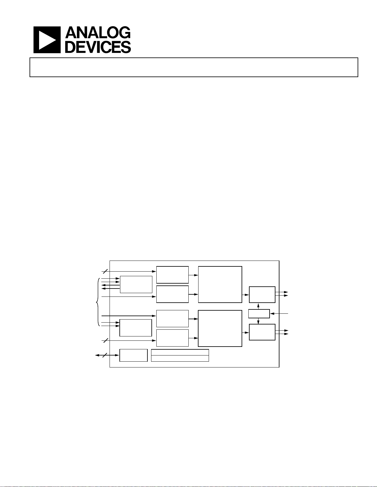
FUNCTIONAL BLOCK DIAGRAM
SERIAL
INPUTA
CLOCK
SIGNAL
GROUP
SERIAL
INPUT B
SPI I/O
GROUP
3
PLL DIVIDERS
PLL DIVIDERS
3
4
SPI PORT
SERIAL
INPUT
CLOCK
DOUBLER
CLOCK
DOUBLER
SERIAL
INPUT
CONTROL REGISTERS
PARAMETER RAM
Figure 1. Functional Block Diagram
BTSC
ENCODER
CORE A
BTSC
ENCODER
CORE B
DAC
BIAS
DAC
AD71028
ENCODED
OUTPUT A
ANALOG
ENCODED
OUTPUT B
04482-0-001
BTSC
BIAS
BTSC
Rev. 0
Information furnished by Analog Devices is believed to be accurate and reliable.
However, no responsibility is assumed by Analog Devices for its use, nor for any
infringements of patents or other rights of third parties that may result from its use.
Specifications subject to change without notice. No license is granted by implication
or otherwise under any patent or patent rights of Analog Devices. Trademarks and
registered trademarks are the property of their respective owners.
One Technology Way, P.O. Box 9106, Norwood, MA 02062-9106, U.S.A.
Tel: 781.329.4700 www.analog.com
Fax: 781.326.8703 © 2004 Analog Devices, Inc. All rights reserved.
Page 2

AD71028
TABLE OF CONTENTS
Specifications..................................................................................... 3
DAC Analog Performance........................................................... 3
BTSC Encoder Performance ....................................................... 3
Digital I/O ..................................................................................... 3
Power.............................................................................................. 4
Temperature Range ...................................................................... 4
Digital Timing............................................................................... 4
Absolute Maximum Ratings............................................................ 5
Pin Configuration and Functional Descriptions.......................... 6
Features .............................................................................................. 8
Pin Functions ................................................................................ 8
Signal Processing ............................................................................ 10
Background of BTSC ................................................................. 10
Performance Factors .................................................................. 10
Separation Alignment................................................................ 10
Input Levels ................................................................................. 11
Clock Relationships.................................................................... 11
SPI Port ............................................................................................ 12
Overview ..................................................................................... 12
SPI Address Decoding ............................................................... 12
Parameter RAM.......................................................................... 13
Control Register ......................................................................... 13
Output Level Register ................................................................ 13
Stereo Enhancement Register................................................... 13
Dialog Enhancement Register.................................................. 13
SPI Read/Write Data Formats .................................................. 14
Initialization ................................................................................ 14
Serial Data Input Port................................................................ 14
Analog Output Section .................................................................. 16
Outline Dimensions....................................................................... 17
Phase Linearity of the External Analog Filter......................... 11
REVISION HISTORY
Revision 0: Initial Version
Ordering Guide .......................................................................... 17
Rev. 0 | Page 2 of 20
Page 3

AD71028
SPECIFICATIONS
TEST CONDITIONS, UNLESS OTHERWISE NOTED
Supply Voltages (AV
, DVDD) 5.0 V
DD
Ambient Temperature 25°C
Input Clock 12.288 MHz
Input Signal 1 kHz, 0 dBFS
Input Sample Rate 48 kHz
Measurement Bandwidth 20 Hz to 14 kHz
Word Width 24 Bits
Load Capacitance 50 pF
Input Voltage HI 2.4 V
Input Voltage LO 0.4 V
DAC ANALOG PERFORMANCE
Table 1.
Parameter Min Typ Max Unit
Resolution 24 Bits
Dynamic Range (20 Hz to 14 kHz, –60 dB Input) (Encoded Output, Left = Right) 85 921 dB
Total Harmonic Distortion + Noise (Encoded Output, Left = Right, 20 Hz to 14 kHz)
VIN = 0 dB –85 –921 dB
Differential Output Range (± Full Scale, Left = Right) 1.7 V p-p
1
Measurement of encoded BTSC signal, not a measurement of end-to-end system.
BTSC ENCODER PERFORMANCE
Table 2.
Parameter Min Typ Max Unit
Channel Separation
1
30 Hz to 500 Hz 27 dB
500 Hz to 5 kHz 23 dB
5 kHz to 13.5 kHz 16 dB
Frequency Response1
30 Hz to 10 kHz +0.5 –1.0 dB
30 Hz to 13.5 kHz +0.5 –1.5 dB
1
These specifications are measured with a –25 dB, 1 kHz input signal.
DIGITAL I/O
Table 3.
Parameter Min Typ Max Unit
Input Voltage HI (VIH) 2.1 V
Input Voltage LO (VIL) 0.8 V
Input Leakage (IIH @ VIH = 2.4 V) 10 µA
Input Leakage (IIL @ VIL = 0.8 V) 10 µA
High Level Output Voltage (VOH) IOH = 2 mA DVDD – 0.5 V
Low Level Output Voltage (VOL) IOL = 2 mA 0.4 V
Rev. 0 | Page 3 of 20
Page 4

AD71028
POWER
Table 4.
Parameter Min Typ Max Unit
Supplies
Voltage, Analog and Digital 4.5 5 5.5 V
Analog Current 31 37 mA
Digital Current 97 110 mA
Dissipation
Operation—Both Supplies 640 mW
Operation—Analog Supplies 155 mW
Operation—Digital Supplies 485 mW
TEMPERATURE RANGE
Table 5.
Parameter Min Typ Max Unit
Specifications Guaranteed 25 °C
Functionality Guaranteed 0 70 °C
Storage –55 +125 °C
DIGITAL TIMING
Table 6.
Parameter Min Typ Max Unit
t
t
t
t
t
t
t
t
t
t
t
t
t
t
t
DMD
DBL
DBH
DLS
DLH
DDS
DDH
CCL
CCH
CLS
CLH
CLD
CDS
CDH
RLP
MCLK Recommended Duty Cycle @ 12.288 MHz (256 × fS and 512 × fS Modes) 40 60 %
BCLK Low Pulse Width 25 ns
BCLK High Pulse Width 10 ns
LRCLK Setup 0 ns
LRCLK Hold 10 ns
SDATA Setup 0 ns
SDATA Hold 10 ns
CCLK Low Pulse Width 10 ns
CCLK High Pulse Width 10 ns
CLATCH Setup 10 ns
CLATCH Hold 20 ns
CLATCH High Pulse Width 10 ns
CDATA Setup 0 ns
CDATA Hold 10 ns
Reset LO Pulse Width 10 ns
Rev. 0 | Page 4 of 20
Page 5
AD71028
ABSOLUTE MAXIMUM RATINGS
Table 7. AD71028 Stress Ratings
Parameter Min Max Unit
DVDD to DGND –0.3 +6 V
ODVDD to DGND –0.3 +6 V
AVDD to AGND –0.3 +6 V
Digital Inputs DGND – 0.3 DVDD + 0.3 V
Analog Inputs AGND – 0.3 AVDD + 0.3 V
AGND to DGND –0.3 +0.3 V
Reference Voltage (AVDD + 0.3)/2 V
Maximum Junction
Temperature
Storage Temperature
Range –65 +150 °C
Soldering 300 °C
10 sec
125 °C
Table 8. Package Characteristics (48-Lead LQFP)
Parameter Min Typ Max Unit
θJA Thermal Resistance
[Junction-to-Ambient]
θJC Thermal Resistance
[Junction-to-Case]
72 °C/W
19.5 °C/W
Stresses above those listed under Absolute Maximum Ratings
may cause permanent damage to the device. This is a stress
rating only; functional operation of the device at these or any
other conditions above those listed in the operational sections
of this specification is not implied. Exposure to absolute
maximum rating conditions for extended periods may affect
device reliability.
ESD CAUTION
ESD (electrostatic discharge) sensitive device. Electrostatic charges as high as 4000 V readily accumulate on
the human body and test equipment and can discharge without detection. Although this product features
proprietary ESD protection circuitry, permanent damage may occur on devices subjected to high energy
electrostatic discharges. Therefore, proper ESD precautions are recommended to avoid performance
degradation or loss of functionality.
Rev. 0 | Page 5 of 20
Page 6
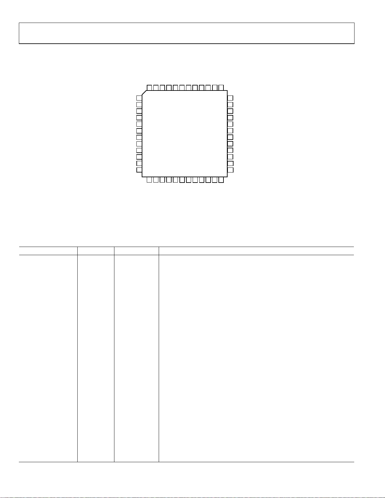
AD71028
A
PIN CONFIGURATION AND FUNCTIONAL DESCRIPTIONS
FILTCAP
REFCAP
NC
38 37
22
23
24
BCLK_PB
LRCLK_PB
SDATA_PB
DIV2_P
DIV1_PB
DIV2_PB
NC
NC
DGND
DVDD
ODVDD
NC
NC
COUT
CDATA
DIV1_PA
48 47 46 45 44
1
2
3
4
5
6
7
8
9
10
11
12
13
DVDD
14
MCLK_PB
15
CCLK
PLL_PB
DVDD
(Not to Scale)
16
DGND
CLATCH
DGND
MCLK_PA
PLL_PA
43 42 41 40 39
AD71028
TOP VIEW
17
18
19
DVDD
RESETB
SDATA_PA
CLK27_PB
CLK27_PA
20
21
BCLK_PA
LRCLK_PA
36
35
34
33
32
31
30
29
28
27
26
25
AGND
OUTB–
OUTB+
AVDD
AGND
AVDD
OUTA+
OUTA–
AGND
NC
NC
DOUBLE
04482-0-002
NC = NO CONNECT
Figure 2. 48-Lead Low Profile Quad Flat Pack (LQFP)
Table 9. Pin Function Descriptions
Pin No. Mnemonic Input/Output Description
1 DIV2_PA OUT CLK27_PA clock (Pin 40) Divided by 1125
2 DIV1_PB OUT PLL_PB Clock (Pin 46) Divided by 512 (DOUBLE = 1) or 1024 (DOUBLE = 0)
3 DIV2_PB OUT CLK27_PB Clock (Pin 41) Divided by 1125
4, 5, 9, 10, 26, 27, 39 NC No Connection
6, 16, 44 DGND Digital Ground
7, 13, 17, 45 DVDD Digital Supply for DSP Core
8 ODVDD Digital Supply for Output Buffers
11 COUT OUT SPI Readback
12 CDATA IN SPI Control Data Input
14 CCLK IN SPI Serial Bit Clock
15 CLATCH IN SPI Control Latch Signal
18 RESETB IN Reset Signal for Both Processors, Active Low
19 SDATA_PA IN Data Input to Processor A
20 BCLK_PA IN Bit Clock Signal for Serial Data Input to Processor A
21 LRCLK_PA IN Left/Right Framing Signal for Data Input to Processor A
22 SDATA_PB IN Data Input to Processor B
23 BCLK_PB IN Bit Clock Signal for Serial Data Input to Processor B
24 LRCLK_PB IN Left/Right Framing Signal for Data Input to Processor B
25 DOUBLE IN Enables Internal Clock Doubler for 12.288 MHz Input (Both Processors)
28, 32, 36 AGND Analog Ground
29 OUTA– OUT Negative Analog Output, Processor A
30 OUTA+ OUT Positive Analog Output, Processor A
31, 33 AVDD Analog Supply
34 OUTB+ OUT Positive Analog Output, Processor B
35 OUTB– OUT Negative Analog Output, Processor B
37 REFCAP IN Connection Point for 10 µF VREF Filter Capacitor
38 FILTCAP IN Connection for Noise Reduction Capacitor
Rev. 0 | Page 6 of 20
Page 7

AD71028
Pin No. Mnemonic Input/Output Description
40 CLK27_PA IN Input for 27 MHz Video Reference Clock, Processor A
41 CLK27_PB IN Input for 27 MHz Video Reference Clock, Processor B
42 PLL_PA IN Input from External PLL, Processor A
43 MCLK_PA IN Clock Input to Processor A
46 PLL_PB IN Input from External PLL, Processor B
47 MCLK_PB IN Clock Input to Processor B
48 DIV1_PA OUT PLL_PA Clock (Pin 42) Divided by 512 (DOUBLE = 1) or 1024 (DOUBLE = 0)
Rev. 0 | Page 7 of 20
Page 8

AD71028
FEATURES
The AD71028 is comprised of two independent digital-input
BTSC encoders. The two processors allow two completely
asynchronous BTSC channels to be encoded, each with its own
clock signals. Figure 1 shows the block diagram of the device.
Signal processing parameters are stored in a 256-location
parameter RAM, which is initialized on power-up by an internal
boot ROM. The values stored in the parameter RAM control all
the filter coefficients, mixing, and dynamics processing code
used in the BTSC algorithm.
The AD71028 has an SPI port that supports complete read/
write capability of the parameter RAM, as well as a control port
and several other registers that allow the various signal processing parameters to be controlled. The AD71028 can run as a
standalone processor without SPI control.
The AD71028 has a very flexible serial data input port that
allows for glueless interconnection to a variety of signal sources.
The AD71028 can be configured in left-justified, I
justified, or DSP serial port compatible modes. It can support
16, 20, and 24 bits in all modes. The AD71028 accepts serial
audio data in MSB first, twos complement format.
The AD71028 operates from a single 5 V power supply. It is fabricated on a single monolithic integrated circuit and is housed
in a 48-lead LQFP package for operation over the 0°C to 70°C
temperature range.
PIN FUNCTIONS
Pin names and functions are shown below. Note that pins with a
“_PA” designation are connected to Processor A, while those
with a “_PB” designation are connected to Processor B. All input
pins have a logic threshold compatible with TTL input levels,
and may therefore be used in systems with 3.3 V logic. All
digital output levels are controlled by the ODVDD pin, which
may range from 2.7 V to 5.5 V, for compatibility with a wide
range of external devices.
LRCLK_PA, LRCLK_PB
Left/right clocks for framing the input data. The interpretation
of the LRCLK changes according to the serial mode, set by
writing to the control registers.
BCLK_PA, BCLK_PB
Serial bit clocks for clocking in the serial data. The interpretation of BCLK changes according to the serial mode, which is set
by writing to the control registers.
SDATA_PA, SDATA_PB
Serial data inputs to each processor. The serial format is selected
by writing to Bits <3:0> of the control registers.
2
S, right-
MCLK_PA, MCLK_PB
Master clock inputs. The master clock frequency must be either
or 512 × fS, where fS is the input sampling frequency. If
256 × f
S
the DOUBLE pin is high, an internal clock doubler is used to
take a 256 × f
input clock and produce the 512 × fS internal
S
clock required by the DSP core. If the DOUBLE pin is low, the
frequency of the input clock must be set to 512 × f
. In case
S
these clock signals are not available, a simple external PLL may
be used to generate the master clock signals. On-chip dividers
are provided to simplify this task.
CDATA
Serial data in for the SPI control port. See the SPI Port section
for more information on SPI port timing.
COUT
Serial data output. This is used for reading back registers and
memory locations. It is three-stated when an SPI read is not
active. See the SPI Port section for more information on SPI
port timing.
CCLK
SPI bit-rate clock. This pin may either run continuously or be
gated in between SPI transactions. See the SPI Port section for
more information on SPI port timing.
CLATCH
SPI latch signal. This signal must go low at the beginning of an
SPI transaction and high at the end of a transaction. Each SPI
transaction may take a different number of CCLKs to complete,
depending on the address and read/write bit that are sent at the
beginning of the SPI transaction. Detailed SPI timing information can be found in the SPI Port section.
RESETB
Active-low reset signal. After RESETB transitions from low to
high, the AD71028 goes through an initialization sequence
where the parameter RAMs are initialized with the contents of
the on-board boot ROM. All SPI registers are set to 0, and the
data RAMs are also zeroed. The initialization is complete after
1024 MCLK cycles. New values should not be written to the SPI
port until the initialization is complete.
DOUBLE
When this pin is set high, the internal clock doubler is turned
on so a 256 × f
MCLK can be input to the AD71028.
S
PLL_PA, PLL_PB
PLL clock input pins for Processor A and Processor B. These
pins are connected to an internal divide-by-1024 circuit (or
divide-by-512 if DOUBLE is high). This makes it possible to use
an inexpensive external PLL to generate the system clock. If an
external PLL is used, this pin should also be connected to the
appropriate MCLK_PA or MCLK_PB pin.
Rev. 0 | Page 8 of 20
Page 9

AD71028
CLK27_PA, CLK27_PB
Input pins to the divide-by-1125 block. If an external PLL is
used to generate the audio master clock, the 27 MHz video
master clock may be applied to these pins where it is divided by
1125 to produce a 24 kHz feedback clock to the external PLL
phase detector.
DIV1_PA, DIV1_PB
Output of divide-by-1024 circuit. Divides the master clock
signal by 1024 (or 512 when DOUBLE is asserted). Used to
interface to external PLL.
DIV2_PA, DIV2_PB
Output of divide-by-1125 circuit. Divides the master-clock
signal by 1125. Used to interface to external PLL. The output
signal is a pulse with a duration of one master clock, and should
therefore be used with edge-triggered phase detectors.
REFCAP
Analog reference voltage input. The nominal REFCAP input
voltage is 2.5 V; the analog gain scales directly with the voltage
on this pin. Any ac signal on this pin will cause distortion, and
therefore a large decoupling capacitor should be used to ensure
that the voltage on REFCAP is clean. The input impedance of
REFCAP is greater than 1 MΩ.
FILTCAP
Filter cap point. This pin is used to reduce the noise on an
internal biasing point in order to provide the highest
performance. It may not be necessary to connect this pin,
depending on the quality of the layout and grounding used in
the application circuit.
DVDD
Digital VDD for core. 5 V nominal.
ODVDD
Digital VDD for all digital outputs. Variable from 2.7 V to 5.5 V.
DGND
Digital ground.
AVDD
Analog VDD. 5 V nominal. Bypass capacitors should be placed
close to the pins and connected directly to the analog ground
plane.
AGND
Analog ground.
OUTA+, OUTA–
Differential analog outputs for Processor A. The nominal output
voltage for a 1 kHz 0 dB mono input signal is 600 mV rms. This
level may be adjusted by writing to SPI location 258.
OUTB+, OUTB–
Differential analog outputs for Processor B. The nominal output
voltage for a 1 kHz 0 dB mono input signal is 600 mV rms. This
level may be adjusted by writing to SPI location 770.
Rev. 0 | Page 9 of 20
Page 10

AD71028
SIGNAL PROCESSING
L– R
COMPRESSOR
L
R
MATRIX
L + R
PRE-EMPHASIS
75µs
FILTER
Figure 3. Signal Processing Flow
BACKGROUND OF BTSC
BTSC is the name of the standard for adding stereo audio
capability to the US television system. It is in many ways similar
to the algorithm used for FM stereo broadcasts, with the
addition of a sophisticated compressor circuit to improve the
signal-to-noise ratio.
The processing of mono (L = R) signals is unchanged from the
original pre-BTSC system in order to maintain compatibility
with non-BTSC TV receivers. The L + R signal is applied to a
75 µs pre-emphasis filter, and is then applied to a 4.5 MHz FM
modulator, which is later added into the video signal to create a
composite video signal.
Stereo capability is added by taking the L–R signal, applying it
to a 2-band dynamic compressor, and then multiplying this
signal by a carrier signal at twice the horizontal scanning rate
), or about 2 × 15.734 kHz. This multiplication is known as
(F
h
double-sideband suppressed-carrier modulation, and it
effectively translates the compressed L – R spectrum up in
frequency so that it sits above the audio band (Figure 3).
In order for the receiver to recover this L – R signal, a pilot tone
at the horizontal rate is added to the signal. The receiver has a
PLL that locks to this pilot and generates a signal at the carrier
frequency. This signal is then used to multiply the composite
BTSC-encoded signal, which translates this component back
down to baseband. The L – R signal is then applied to a 2-band
expander, which is the complement to the earlier compressor
step. Once the L + R and L – R signals are recovered, a simple
addition/subtraction circuit (sometimes referred to as the
“matrix”) can be used to recover the L and R signal.
Since the pilot tone is added at 15.734 kHz, it is necessary to
reduce the signal’s bandwidth so that audio signals cannot
interfere with the pilot tone. In the AD71028, the bandwidth is
limited to 14 kHz; above this frequency, the response decays
very rapidly.
OSCILLATOR
2× Fh CARRIER
Fh PILOT
TO
DAC
04482-0-003
PERFORMANCE FACTORS
In order to maintain good separation between left and right, it is
necessary to closely match the filtering and companding standards set forth in the standard (FCC OET60). Even small errors
can result in poor performance. The AD71028 has been programmed to match these standards as accurately as possible.
Separation typically ranges from 30 dB at frequencies below
1 kHz to 15 dB at 14 kHz. Measuring these numbers can be
difficult as significant differences exist between many so-called
reference decoders, which are all implemented with analog
components.
SEPARATION ALIGNMENT
The BTSC encoder outputs are all specified in terms of the
deviation of the FM 4.5 MHz carrier. For the AD71028, a digital
input level of 0 dB (mono signal) should cause a carrier
deviation of ±25 kHz without the 75 µs pre-emphasis filter. In
practice, the pre-emphasis filter may be left in for this adjustment, as long as the frequency is low enough to not be affected
by the pre-emphasis filter. It is critical to maintain the proper
gain relationship between the BTSC encoder and the 4.5 MHz
FM modulator. A common mistake is to assume that changing
the gain between the BTSC encoder output and the FM
modulator input has the same effect as changing the audio
input level going in to the BTSC encoder. The presence of a
complicated 2-band nonlinear dynamics processor means that
the encoder output must be connected to the decoder input
(through the FM modulation/demodulation process) with a
known gain. If this gain is changed, the separation will
significantly suffer.
When measuring the AD71028 on the bench, it is possible to
use a BTSC reference decoder box, so that the FM modulation/
demodulation process may be skipped. These units have a
method of adjusting the input voltage sensitivity to achieve best
separation. The output level of the AD71028 can also be
adjusted over a wide range using either the SPI control port or
by adjusting the values of the components used in the external
analog low-pass filter that is between the BTSC encoder output
and the input to the FM modulator.
Rev. 0 | Page 10 of 20
Page 11

AD71028
PHASE LINEARITY OF THE EXTERNAL ANALOG FILTER
If the time alignment of the pilot to the carrier signal is not
close to 0 degrees, a loss of separation can occur. This means
that the external analog low-pass filter should be a linear-phase
design to provide constant group delay over the range from dc
to 50 kHz. Bessel filters are recommended for this application.
Figure 12 shows a recommended design for these filters.
INPUT LEVELS
The maximum input level to the AD71028 changes across
frequency. Table 10 shows the maximum allowable input level
for different frequencies. These values are part of the BTSC
specification and are not a function of this chip.
Table 10. Maximum Input Levels to the BTSC Encoder
across Frequency
Frequency (Hz) Maximum Input Level (dBFS)
20 to 1000 0 dB
1600 –1 dB
2500 –3 dB
3150 –5 dB
5000 –8 dB
8000 –11 dB
12500 –15 dB
CLOCK RELATIONSHIPS
In an MPEG receiver architecture, all clocks are typically
generated from a 27 MHz master clock. The following integer
relationships are found between the clocks, with F
15.734 kHz:
a) 27 MHz/F
/2 = F
b) F
h
= 1716 = 2 × 2 × 3 × 11 × 13
h
color_subcarrier
/(5 × 7 × 13)
=
h
The AD71028 contains a clock doubler circuit that may be used
to generate an internal 512 × f
. The clock mode is set by connecting the DOUBLE pin
256 × f
S
clock when the external clock is
S
either high or low. This pin should be tied either high or low
and should not be changed after power-up.
The AD71028 requires a master clock at either 256 × 48 kHz
(12.288 MHz) when DOUBLE = 1 or 512 × 48 kHz
(24.576 MHz) when DOUBLE = 0. In some cases, this signal is
provided by the MPEG decoder chip itself. In other cases, only
the 27 MHz video clock may be available. In this case, the
AD71028 provides on-chip dividers to interface to an external
PLL such as the 74HC4046. Figure 4 shows the circuit to
accomplish this. The 27 MHz clock is applied to the AD71028
and divided down by 1125, producing a signal at 24 kHz. The
PLL oscillator output is divided down by 512, producing a
24 kHz output (when locked). These two signals are applied to
the phase-comparator inputs of the external PLL. Note that the
divided-down 27 MHz signal looks like a pulse with a duration
of one master clock, and therefore only edge-triggered phase
detectors should be used.
AD71028
27MHz IN
74HC4046
Figure 4. PLL Connections for 27 MHz Master Clock
DIVIDE-BY-1125
DIVIDE-BY-512
DSP
04482-0-004
c) 27 MHz/F
color_subcarrier
d) 27 MHz/48 kHz = 1125/2
= (5 × 7)/(2 × 2 × 2 × 3 × 11)
Rev. 0 | Page 11 of 20
Page 12

AD71028
SPI PORT
CLATCH
CCLK
CDATA
CLATCH
CCLK
CDATA
COUT
HI-Z
BYTE 0
Figure 5. Sample of SPI Write Format (Single-Write Mode)
Figure 6. Sample of SPI Read Format (Single-Read Mode)
OVERVIEW
The AD71028 can be controlled using the SPI port. In general,
there are three parameters per processor that can be controlled:
the encoder output level, the Phat Stereo image enhancement
algorithm, and the dialog enhancement algorithm. It is also
possible to write new data into the parameter RAM to alter the
filter coefficients used in the BTSC encoding process. This is a
fairly complex topic unnecessary for normal operation of the
chip, and the details are not included in this data sheet. Please
contact ADI if modifications to the BTSC filters are required.
The SPI port uses a 4-wire interface consisting of CLATCH,
CCLK, CDATA, and COUT signals. The CLATCH signal goes
low at the beginning of a transaction and high at the end of a
transaction. The CCLK signal latches the serial input data on a
low-to-high transition. The CDATA signal carries the serial
input data, and the COUT signal is the serial output data. The
BYTE 1 BYTE 4
XXXBYTE 0 BYTE 1
HI-Z
DATA
DATA
DATA
04482-0-006
COUT signal remains three-stated until a READ operation is
requested. This allows other SPI compatible peripherals to share
the same readback line. All SPI transactions follow the same
basic format, shown in Figure 5. Figure 6 shows the read format.
The Wb/R bit is low for a write and high for a read operation.
The 10-bit address word is decoded into either a location in the
parameter RAM or one of the SPI registers. The number of data
bytes varies according to the register or memory being accessed.
The detailed data format diagram for continuous-mode
operation is given in the SPI Read/Write Data Formats section.
SPI ADDRESS DECODING
Table 11 shows the address decoding used in the SPI port. The
SPI address space encompasses a set of registers and the parameter RAM. The parameter RAM is loaded on power-up from an
on-board boot ROM.
Table 11. SPI Port Address Decoding
SPI Address Register Name Read/Write Word Length
0–255 Parameter RAM Processor A Write: 22 Bits, Read: 22 Bits
256 SPI Control Register Processor A Write: 11 Bits, Read: N/A
257 Reserved
258 Output Level Processor A Write: 22 Bits, Read: N/A
259 Stereo Spreading Control Processor A Write: 22 Bits, Read: N/A
260 Dialog Enhancement Control Processor A Write: 22 Bits, Read: N/A
512–767 Parameter RAM Processor B Write: 22 Bits, Read: 22 Bits
768 SPI Control Register Processor B Write: 22 Bits, Read: N/A
769 Reserved
770 Output Level Processor B Write: 22 Bits, Read: N/A
771 Stereo Spreading Control Processor B Write: 22 Bits, Read: N/A
772 Dialog Enhancement Control Processor B Write: 22 Bits, Read: N/A
04482-0-005
Rev. 0 | Page 12 of 20
Page 13

AD71028
PARAMETER RAM
The parameters for the two BTSC processors are stored in two
256-location RAM spaces. The user should not change most of
these parameters, although editing the dynamics processing
curve for dialog enhancement may be useful if the curve needs
to be changed for a specific application. This is explained in the
Dialog Enhancement Register section of this data sheet.
CONTROL REGISTER
Control Register 1 is an 11-bit register that controls serial
modes, de-emphasis, mute, power-down, and SPI-to-memory
transfers. Table 12 documents the contents of this register.
Bits 4:5 and 8:10 are reserved and should be set to 0 at all times.
The audio signal is muted with Bit 7 of the control register.
The soft power-down bit (Bit 6) stops the internal clocks to the
DSP core, but does not reset the part. The digital power consumption is reduced to a low level when this bit is asserted.
Reset can only be asserted using the external reset pin.
Bits 3:2 select the serial format from one of four modes. These
different formats are discussed in the Initialization section of
this data sheet.
The word length bits (1:0) are used in right-justified serial
modes to determine where the MSB is located relative to the
start of the audio frame.
Table 12. Control Register Contents
Register Bits Function
10 Reserved, Set to 0
9 Reserved, Set to 0
8 Reserved, Set to 0
7 Soft Mute (1 = Start Mute Sequence)
6 Soft Power-Down (1 = Power-Down)
5:4 Reserved, Set to 00
3:2 Serial In Mode
00 = I2S
01 = Right-Justified
10 = DSP
11 = Left-Justified
1:0 Word Length
00 = 24 Bits
01 = 20 Bits
10 = 16 Bits
11 = 16 Bits
OUTPUT LEVEL REGISTER
The output level register controls the overall BTSC output level.
Its default value is –6 dB, which outputs a 600 mV rms reference
level for a 1 kHz 0 dB mono digital input signal. This value is in
2.20 format, and –6 dB corresponds to binary
0010000000000000000000. This register is used in conjunction
with the output filter to match the output BTSC level of the
encoder with the decoder input to achieve maximum separation
values. This level control should not be used to control the
overall volume level of the audio signal.
STEREO ENHANCEMENT REGISTER
This register controls ADI’s patented Phat Stereo spatial
enhancement algorithm. The default is all 0s, which corresponds to no effect. The maximum setting is
0100000000000000000000, or a twos complement fractional
value of 1.0. Note that the bass energy in each channel is
increased using this algorithm, which may cause some digital
clipping on full-scale signal peaks, especially at low frequencies.
DIALOG ENHANCEMENT REGISTER
This controls the built-in dialog-enhancement algorithm, and
defaults to 0. The maximum setting is
0100000000000000000000, or a twos complement fractional
value of 1.0. This algorithm is intended to solve the problem of
playing back high dynamic range digital audio signals over a
television’s built-in speakers. It provides an amplitude boost to
signals that are in the range where dialog signals are usually
found, while at the same time preventing loud special effects
passages from overloading the speakers or amplifiers.
The dialog enhancement control is set up as a dynamics
processing curve with 33 locations on the curve, each spaced
3 dB apart. There is a default dialog enhancement curve that is
set at power-up, but this can be changed if a different curve is
desired. The curve ranges from an rms input level of –87 dB on
the low end to +9 dB on the high end. The value corresponding
to each point in the parameter RAM represents a gain at the
appropriate input level. This gain value should range from 0
(–∞ dB) to +2.0 – 1 LSB (approximately +6 dB). The gain at a
–87 dB input corresponds to parameter RAM location 4 on
Processor A and location 516 on Processor B. The table extends
to the +9 dB input gain at locations 36 and 548 for Processors A
and B, respectively.
Rev. 0 | Page 13 of 20
Page 14

AD71028
Table 13. SPI Control Register 1 Write format
Byte 0 Byte 1 Byte 2 Byte 3
00000, Wb/R, Adr [9:8] Adr [7:0] 00000, Bit [10:8] Bit [7:0]
Table 14. SPI Write Format for Parameter RAM, Output Level, Stereo Spreading and Dialog Enhancement Registers
Byte 0 Byte1 Byte 2 Byte 3 Byte 4
000000, Adr [9:8] Adr [7:0] 00, Level [21:16] Level [15:8] Level [7:0]
SPI READ/WRITE DATA FORMATS
The read/write formats of the SPI port are designed to be byteoriented. This allows for easy programming of common microcontroller chips. In order to fit into a byte-oriented format, 0s
are appended to the data fields in order to extend the data-word
to the next multiple of 8 bits. For example, 22-bit words written
to the SPI parameter RAM are appended with two leading zeros
in order to reach 24 bits (3 bytes). These zero-extended data
fields are appended to a 2-byte field consisting of a read/write
bit and a 10-bit address. The SPI port knows how many data
bytes to expect based on the address that is received in the first
2 bytes.
INITIALIZATION
Power-Up Sequence
The AD71028 has a built-in power-up sequence that initializes
the contents of all internal RAM. During this time, the SPI
parameter RAM is filled with values from its associated boot
ROM. The data memories are also cleared during this time.
Serial Data Input Modes
Figure 7 shows the left-justified mode. LRCLK is high for the
left channel and low for the right channel. Data is sampled on
the rising edge of BCLK. The MSB is left-justified to a LRCLK
transition with no MSB delay. The left-justified mode can accept
any word length up to 24 bits.
2
Figure 8 shows the I
S mode, which is the default setting.
LRCLK is low for the left channel, and the MSB is delayed from
the edge of the LRCLK by a single BCLK period. The I
can be used to accept any number of bits up to 24.
Figure 9 shows the AD71028’s right-justified mode. LRCLK is
high for the left channel and low for the right channel. Data is
sampled on the rising edge of BCLK. The start of data is delayed
from the LRCLK edge by 16, 12, or 8 BCLK intervals, depending
on the selected word length. The default word length is 24 bits;
other word lengths are set by writing to Bits <1:0> of the control
register. In right-justified mode, it is assumed that there are 64
BCLKs per frame.
2
S mode
The boot sequence lasts for 1024 MCLK cycles and starts on the
rising edge of the RESETB pin. The user should avoid writing to
or reading from the SPI registers during this period of time.
SERIAL DATA INPUT PORT
The AD71028’s flexible serial data input port accepts data in
twos complement, MSB-first format. The left channel data field
always precedes the right channel data field. The serial mode is
set by using mode select bits in the SPI control register. In all
modes except the right-justified mode, the serial port will
accept an arbitrary number of bits up to a limit of 24 (extra bits
will not cause an error, but they will be truncated internally). In
right-justified mode, SPI control register bits are used to set the
word length to 16, 20, or 24 bits. The default on power-up is
24-bit mode. Proper operation of the right-justified mode
requires that there be exactly 64 BCLKs per audio frame.
Figure 10 shows the DSP serial port mode. LRCLK must pulse
high for at least one bit clock period before the MSB of the left
channel is valid, and LRCLK must pulse high again for at least
one bit clock period before the MSB of the right channel is
valid. Data is sampled on the falling edge of BCLK. The DSP
serial port mode can be used with any word length up to 24 bits.
In this mode, it is the responsibility of the DSP to ensure that
the left data is transmitted with the first LRCLK pulse, and that
synchronism is maintained from that point forward.
Rev. 0 | Page 14 of 20
Page 15

AD71028
S
A
A
LRCLK
BCLK
SDATA
LRCLK
LRCLK
BCLK
SDATA
MSB LSB
BCLK
DAT
MSB
MSB LSB
LEFT CHANNEL
MSB
1 /F
S
Figure 7. Left-Justified Mode—16 Bits to 24 Bits per Channel
LEFT CHANNEL
LSB
1 /F
S
2
Figure 8. I
S Mode—16 Bits to 24 Bits per Channel
LEFT CHANNEL
1 /F
S
Figure 9. Right-Justified Mode—16 Bits to 24 Bits per Channel
MSB
RIGHT CHANNEL
RIGHT CHANNEL
RIGHT CHANNEL
MSB
LSB
LSB
LSB
04482-0-007
04482-0-008
04482-0-009
LRCLK
BCLK
SDAT
MSB
LSB
1 /F
S
MSB
Figure 10. DSP Mode—16 Bits to 24 Bits per Channel
NOTES
1. DSP mode does not identify the channel.
2. LRCLK normally operates at F
; in DSP mode, LRCLK operates at 2 × FS.
S
3. BCLK frequency is normally 64 × LRCLK but may be operated in burst mode.
LSB
04482-0-010
Rev. 0 | Page 15 of 20
Page 16

AD71028
O
ANALOG OUTPUT SECTION
Figure 11 shows the block diagram of the analog output section
(one of two channels). A series of current sources is controlled
by a digital Σ-∆ modulator. Depending on the digital code from
the modulator, each current source is connected to the summing junction of either a positive I-to-V converter or a negative
I-to-V converter. Two extra current sources that push instead of
pull are added to set the midscale common-mode voltage.
All current sources are derived from the VREF input pin. The
gain of the AD71028 is directly proportional to the magnitude
of the current sources, and therefore the gain of the AD71028 is
proportional to the voltage on the VREF pin. The nominal
VREF voltage should be set to 2.5 V, using a simple resistive
divider from the analog supply. The VREF and biasing circuits
are common to both DACs.
UT+
FROM DIGITAL
Σ–∆ MODULATOR
(DIG_IN)
I
REF
REF
+ DIG_IN
SWITCHED CURRENT
V
BIAS
SOURCES
Figure 11. Internal DAC Analog Architecture
REF
I
REF
OUT–
IN
I
– DIG_INI
REF
04482-0-011
Since the VREF input effectively multiplies the signal, care must
be taken to ensure that no ac signals appear on this pin. This
can be accomplished by using a large decoupling capacitor in
the VREF external resistive divider circuit. If the VREF signal is
derived by dividing the 5 V analog supply, the time constant of
the divider must effectively filter any noise on the supply. If the
VREF signal is derived from an unregulated power amplifier
supply, the time constant must be longer because the ripple on
the amplifier supply voltage will presumably be greater than in
the case of the 5 V supply.
The AD71028 should be used with an external third-order filter
on each output channel. The circuit shown in Figure 12
combines a third-order filter and a single-ended-to-differential
converter in the same circuit. The values shown are for a
100 kHz Bessel filter. The use of a Bessel filter is important to
maintain the time alignment of the pilot to the carrier. If these
signals are not in phase, a loss of separation will occur.
The outputs can also be used single-ended, with some loss of
performance; the DAC distortion may become significantly
poorer, although the SNR will remain quite high.
For best performance, a large (>10 µF) capacitor should be
connected between the FILTCAP pin and analog ground.
1nF
2.7nF
3.01kΩ
1.50kΩ
499kΩ
1.00kΩ
–INPUT
+INPUT
2.80kΩ
806Ω
Figure 12. Recommended External Analog Filter for Each Channel
270pF
820pF
549Ω
2.2nF
OUT
04482-0-012
Rev. 0 | Page 16 of 20
Page 17

AD71028
OUTLINE DIMENSIONS
1.45
1.40
1.35
0.15
0.05
ROTATED 90°CCW
10°
SEATING
PLANE
VIEW A
0.75
0.60
0.45
SEATING
PLANE
6°
0.20
2°
0.09
7°
°
3.5
0°
0.08 MAX
COPLANARITY
COMPLIANT TO JEDEC STANDARDS MS-026BBC
1.60
MAX
VIEW A
Figure 13. 48-Lead Low Profile Quad Flatpack [LQFP]
(ST-48)
Dimensions Shown in Millimeters
ORDERING GUIDE
Model Temperature Range Package Description Package Option
AD71028JST –0°C to +70°C 48-Lead LQFP ST-48
AD71028JSTRL –0°C to +70°C 48-Lead LQFP ST-48 on 13” Reel
1
12
0.50
BSC
48
13
9.00 BSC
SQ
PIN 1
TOP VIEW
(PINS DOWN)
37
24
0.27
0.22
0.17
36
25
7.00
BSC SQ
Rev. 0 | Page 17 of 20
Page 18

AD71028
NOTES
Rev. 0 | Page 18 of 20
Page 19

AD71028
NOTES
Rev. 0 | Page 19 of 20
Page 20

AD71028
NOTES
© 2004 Analog Devices, Inc. All rights reserved. Trademarks and
registered trademarks are the property of their respective owners.
D04482–0–1/04(0)
Rev. 0 | Page 20 of 20
 Loading...