

Page 1
CMOS
a
FEATURES
Single +5 V Supply
Receive Channel
Differential or Single-Ended Analog Inputs
Auxiliary Set of Analog I & Q Inputs
Two Sigma-Delta A/D Converters
Choice of Two Digital FIR Filters
Root-Raised-Cosine Rx Filters, α = 0.35
Brick Wall FIR Rx Filters
On-Chip or User Rx Offset Calibration
ADC Sampling Vernier
Three Auxiliary DACs
On-Chip Voltage Reference
Low Active Power Dissipation, Typical 45 mW
Low Sleep Mode Power Dissipation, <50 µW
28-Pin SSOP
APPLICATIONS
American TIA Digital Cellular Telephony
American Analog Cellular Telephony
Digital Baseband Receivers
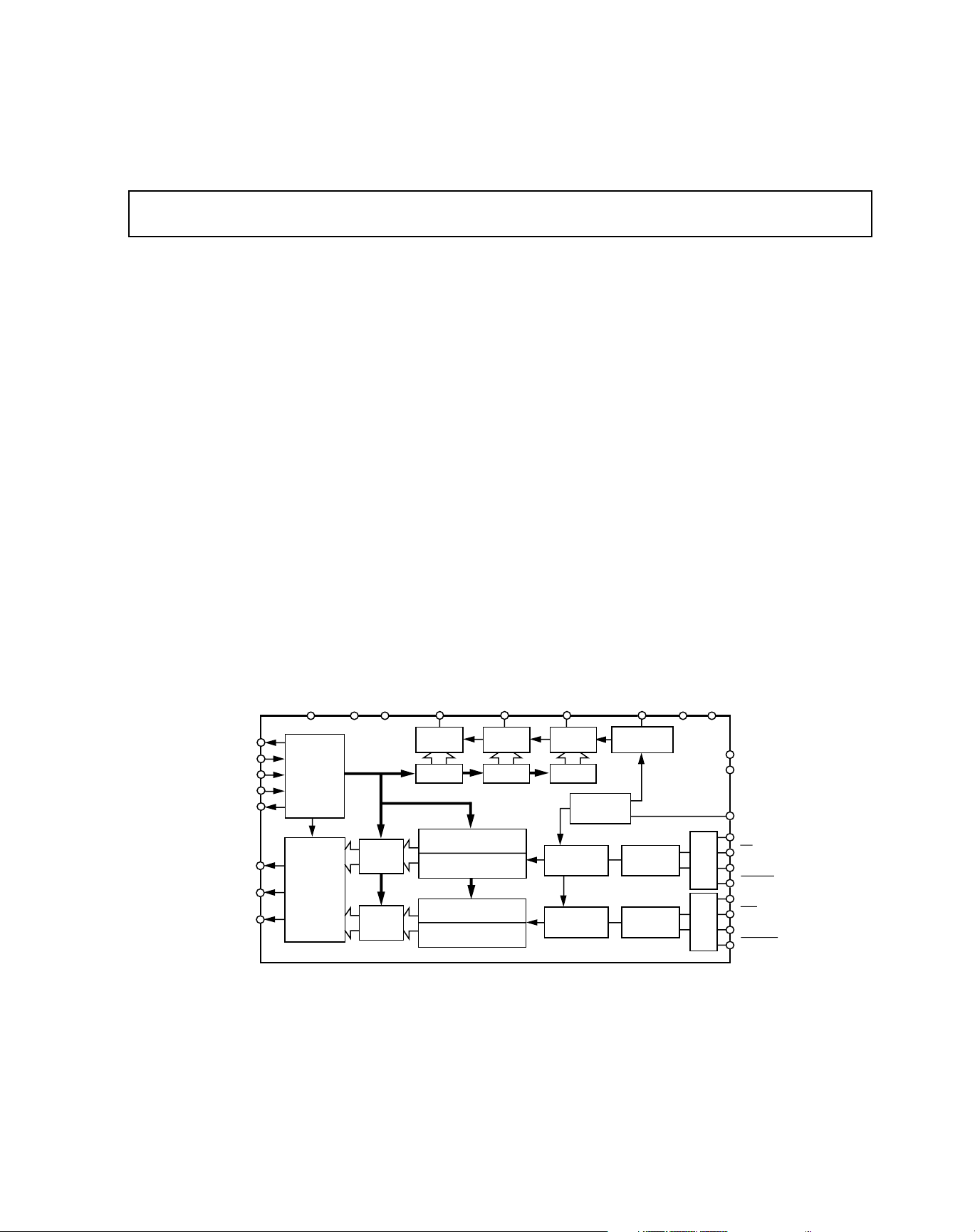
GENERAL DESCRIPTION
The AD7013 is a complete low power, CMOS, TIA IS-54 baseband receive port with single +5 V power supply. The part is
TIA IS-54 Baseband Receive Port
AD7013
designed to perform the baseband conversion of I and Q
waveforms in accordance with the American (TIA IS-54)
Digital Cellular Telephone system.
The receive path consists of two high performance sigma-delta
ADCs, each followed by a FIR digital filter. A primary and
auxiliary set of IQ differential analog inputs are provided,
where either can be selected as inputs to the sigma-delta
ADCs. Also, a choice of two frequency responses are available
for the receive FIR filters; a Root-Raised-Cosine filter for
digital mode or a brick wall response for analog mode.
Differential analog inputs are provided for both I and Q
channels. On-chip calibration logic is also provided to remove
either on-chip offsets or remove system offsets. A 16-bit serial
interface is provided, interfacing easily to most DSPs. The
receive path also provides a means to vary the sampling
instant, giving a resolution to 1/32 of a symbol interval.
The auxiliary section provides two 8-bit DACs and one 10-bit
DAC for functions such as automatic gain control (AGC),
automatic frequency control (AFC) and power amplifier
control.
As it is a necessity for all digital mobile systems to use the
lowest possible power, the device has receive and auxiliary
power down options. The AD7013 is housed in a space
efficient 28-pin SSOP (Shrink Small Outline Package).
FUNCTIONAL BLOCK DIAGRAM
DxCLK
DATA IN
FRAME IN
MODE1
FRAME OUT
Rx CLK
Rx DATA
Rx FRAME
MCLK
INTERFACE
RECEIVE
CHANNEL
INTERFACE
SERIAL
SERIAL
DGND V
OFFSET
ADJUST
OFFSET
ADJUST
AUX DAC1 AUX DAC2 AUX DAC3
DD
10-BIT
AUX DAC
LATCH
ANALOG MODE
FIR DIGITAL FILTER
ROOT RAISED COSINE
FIR DIGITAL FILTER
ANALOG MODE
FIR DIGITAL FILTER
ROOT RAISED COSINE
FIR DIGITAL FILTER
REV. A
Information furnished by Analog Devices is believed to be accurate and
reliable. However, no responsibility is assumed by Analog Devices for its
use, nor for any infringements of patents or other rights of third parties
which may result from its use. No license is granted by implication or
otherwise under any patent or patent rights of Analog Devices.
V
FS ADJUST
8-BIT
AUX DAC
LATCH
One Technology Way, P.O. Box 9106, Norwood. MA 02062-9106, U.S.A.
Tel: 617/329-4700 Fax: 617/326-8703
8-BIT
AUX DAC
LATCH
1.23V
REFERENCE
∆Σ–∆
MODULATOR
∆Σ–∆
MODULATOR
FULL-SCALE
ADJUST
SWITCHED
CAP FILTER
SWITCHED
CAP FILTER
AGND
AA
AD7013
MUX
MUX
AGND
AGND
BYPASS
IRx
IRx
AUX IRx
AUX IRx
QRx
QRx
AUX QRx
AUX QRx
Page 2
AD7013–SPECIFICATIONS
(VAA = VDD = +5 V ± 10%; AGND = DGND = 0 V; f
1
= T
to T
T
A
MIN
, unless otherwise noted)
MAX
= 6.2208 MHz;
MCLK
Parameter AD7013A Units Test Conditions/Comments
RECEIVE SECTION
ADC SPECIFICATION
Number of Input Channels 4 (IRx–IRx) and
QRx–QRx); CR12 = 0
(AUX IRx–AUX IRx) and
(AUX QRx–AUX QRx); CR12 = 1
Number of ADC Channels 2
Resolution 15 Bits
ADC Signal Range 2.6 Volts p-p Measured Using an Input Sine Wave of 3 kHz
Differential Signal Range V
± 0.65 Volts For Both Noninverting and
BIAS
Inverting Analog Inputs
Single-Ended Signal Range V
V
BIAS
± 1.3 Volts For Noninverting Analog Inputs;
BIAS
Inverting Analog Inputs = V
0.65 to (VAA–0.65) Volts min/max Differential
BIAS
1.3 to (VAA–1.3) Volts min/max Single-Ended
Input Range Accuracy ±7.5 %
Accuracy
Bias Offset Error ±7.5 mV Autocalibration; V
= min/max
BIAS
±55 mV User Calibration; I & Q Offset
Adjust Registers Equal to Zero
Dynamic Specifications
CMRR –40 dB typ Measured Using an Input Sine Wave of
3 kHz with Both Noninverting and
Inverting Inputs Tied Together
Dynamic Range 70 dB typ Digital Mode Filter; CR11 = 0
65 dB typ Analog Mode Filter; CR11 = 1
SNR
2
65 dB min Digital Mode Filter; CR11 = 0
68 dB typ
60 dB min Analog Mode Filter; CR11 = 1
63 dB typ
Input Sampling Rate 1.5552/1.28 MHz MCLK = 6.2208 MHz/5.12 MHz; MCLK/4
Output Word Rate 97.2/80 kHz MCLK = 6.2208 MHz/5.12 MHz;
4 × Sampling of the Symbol Rate, MCLK/64
48.6/40 kHz MCLK = 6.2208 MHz/5.12 MHz;
2 × Sampling of the Symbol Rate, MCLK/128
RECEIVE DIGITAL FILTERS
Digital Mode MCLK = 6.2208 MHz
Root-Raised-Cosine α = 0.35
Settling Time 329.2 µs
Absolute Group Delay 164.6 µs
Frequency Response
0–7.8975 kHz ±0.05 dB max
11.9 kHz –3.0 dB
16.4025 kHz –19 dB
> 30 kHz –66 dB max
Analog Mode MCLK = 5.12 MHz
Brick Wall Filter
Settling Time 400 µs
Absolute Group Delay 200 µs
Frequency Response
0–8 kHz 0 to –0.5 dB max
11.4 kHz –3.0 dB
15 kHz –24 dB
>17 kHz –68 dB max
TIA IS-54 RECEIVE SPECIFICATIONS
Error Vector Magnitude
Error Offset Magnitude
3
3
2 % rms typ Measured Using a Full-Scale Input
1 % rms typ
–2–
REV. A
Page 3

Parameter AD7013A Units Test Conditions/Comments
AUXILIARY SECTION
AUX DAC1 AUX DAC2 AUX DAC3
Resolution 10 8 8 Bits
DC Accuracy
Integral ±3 ± 1 ±1 LSBs max
Differential –1.5/+4 ±1 ± 1 LSBs max AUX DAC2 & AUX DAC3 Guaranteed
Monotonic
Zero Code Leakage ±500 ±500 ±500 nA max
Gain Error ±7.5 ±7.5 ±7.5 % max
Output Full-Scale Current 566 280 280 µAR
Output Impedance
4
2MΩ typ
= 18 kΩ
SET
Output Voltage Compliance 2.6 Volts max
Coding Binary
Power Down Option Yes
REFERENCE SPECIFICATIONS
V
REF
1.23 Volts typ
Reference Accuracy ±5 % max
Reference Impedance 20 kΩ typ
LOGIC INPUTS
, Input High Voltage VDD–0.9 V min
V
INH
V
, Input Low Voltage 0.9 V max
INL
, Input Current 10 µA max
I
INH
CIN, Input Capacitance 10 pF max
AD7013
LOGIC OUTPUTS
V
, Output High Voltage VDD–0.4 V min |I
OH
VOL, Output Low Voltage 0.4 V max |I
| ≤ 40 µA
OUT
| ≤ 1.6 mA
OUT
POWER SUPPLIES
V
DD
5
I
DD
4.5/5.5 V
MIN/VMAX
All Sections Active 10.5 mA max CR14 = CR15 = CR16 = CR17 = 1
9 mA typ MCLK = 6.2208 MHz; 80 pF
Load on DxCLK
ADCs Active Only 8.6 mA max CR14 = 1; CR15 = CR16 = CR17 = 0
MCLK = 6.2208 MHz; 80 pF
Load on DxCLK
AUX DACs Active Only 2.2 mA max CR14 = 0; CR15 = CR16 = CR17 = 1;
MCLK Inactive, MCLK = 0 V
10-Bit AUX DAC Active 1.6 mA max CR14 = CR15 = CR16 = 0; CR17 = 1;
MCLK Inactive, MCLK = 0 V
All Sections Powered Down
6
2 mA max CR14 = CR15 = CR16 = CR17 = 0
MCLK = 6.2208 MHz; 80 pF
Load on DxCLK
30 µA typ MCLK =100 kHz; 80 pF
Load on DxCLK
10 µA max MCLK Inactive, MCLK = 0 V
NOTES
1
Operating temperature ranges as follows: A version: –40°C to +85°C.
2
SNR calculation includes noise and distortion components.
3
See Terminology.
4
Sampled tested only.
5
Measured while the digital inputs are static and equal to 0 V or VDD.
6
With all sections powered down, IDD is proportional to the capacitive load on DxCLK. For example, IDD is typically 1.7 mA with 80 pF load and 600 µA with
10 pF load.
Specifications subject to change without notice.
REV. A
–3–
Page 4

AD7013
TERMINOLOGY
Sampling Rate
This is the rate at which the modulators on the receive channels
sample the analog input.
Output Rate
This is the rate at which data words are made available at the
RxDATA pin.
Integral Nonlinearity
This is the maximum deviation from a straight line passing through
the endpoints of the DAC or ADC transfer function.
Differential Nonlinearity
This is the difference between the measured and the ideal 1 LSB
change between any two adjacent codes in the DAC or ADC.
Dynamic Range
Dynamic Range is the ratio of the maximum rms input signal to the
rms noise of the converter, expressed logarithmically, in decibels
(dB = 20 log
[ratio]).
10
Signal to (Noise + Distortion) Ratio
This is the measured ratio of signal to (noise + distortion) at the
output of the receive channel. The signal is the rms amplitude of
the fundamental. Noise is the rms sum of all nonfundamental
signals up to half the sampling frequency (f
/2), excluding dc. The
S
ratio is dependent upon the number of quantization levels in the
digitization process; the more levels, the smaller the quantization
noise. The theoretical signal to (noise + distortion) ratio for a sine
wave is given by:
Signal to (Noise + Distortion) = (6.02N + 1.76) dB
Settling Time
This is the digital filter settling time in the AD7013 receive section.
Bias Offset Error
This is the amount of offset in the receive channel ADC when the
differential inputs are tied together.
Receive Error Vector Magnitude
This is a measure of the rms signal error vector introduced by the
receive Root-Raised Cosine digital filter. This is measured by
applying an ideal transmit signal (i.e., an ideal π/4 DQPSK
modulator and an ideal transmit Root-Raised Cosine filter) to the
receive channel and measuring the resulting rms error vector.
Offset Vector Magnitude
This is a measure of the offset vector introduced by the AD7013 as
illustrated in the figure below. The offset vector is calculated so as to
minimize the rms error vector for each of the constellation points.
ERROR
Q
VECTOR
ABSOLUTE MAXIMUM RATINGS
(TA = +25°C unless otherwise noted)
1
VAA, VDD to GND ......................... –0.3 V to +7 V
AGND to DGND ........................–0.3 V to +0.3 V
Digital I/O Voltage to DGND ........... –0.3 V to V
+0.3 V
DD
Analog I/O Voltage to AGND ........... –0.3 V to VDD +0.3 V
Operating Temperature Range
Industrial (A Version) ................... –40°C to +85°C
Storage Temperature Range ............... –65°C to +150°C
Maximum Junction Temperature ...................+150°C
SSOP θ
Thermal Impedance ....................+122°C/W
JA
Lead Temperature Soldering
Vapor Phase (60 sec) ...........................+215°C
Infrared (15 sec) ..............................+220°C
NOTES
1
Stresses above those listed under “Absolute Maximum Ratings” may cause perma-
nent damage to the device. This is a stress rating only and functional operation of
the device at these or any other conditions above those listed in the operational
sections of this specification is not implied. Exposure to absolute maximum rating
conditions extended periods may affect device reliability.
PIN CONFIGURATION
V
1
AA
IRx
2
IRx
QRx
QRx
AGND
3
4
5
6
AD7013
7
TOP VIEW
8
(Not to Scale)
9
10
11
12
13
14
AUX IRx
AUX IRx
AUX QRx
AUX QRx
MODE1 DATA IN
Rx FRAME
Rx DATA DGND
Rx CLK FRAME OUT
BYPASS
28
AGND
27
FS ADJUST
26
AGND
25
AUX DAC1
24
AUX DAC2
23
AUX DAC3
22
V
21
MCLK
20
DxCLK
19
18
FRAME IN
17
16
15
DD
ORDERING GUIDE
Model Temperature Range Package Option*
AD7013ARS –40°C to +85°C RS-28
*RS = SSOP.
SIGNAL
OFFSET
VECTOR
VECTOR
I
CAUTION
ESD (electrostatic discharge) sensitive device. Electrostatic charges as high as 4000 V readily
accumulate on the human body and test equipment and can discharge without detection. Although
this device features proprietary ESD protection circuitry, permanent damage may occur on devices
subjected to high energy electrostatic discharges. Therefore, proper ESD precautions are recommended to avoid performance degradation or loss of functionality.
–4–
WARNING!
ESD SENSITIVE DEVICE
REV. A
Page 5

AD7013
PIN FUNCTION DESCRIPTIONS
SSOP Pin
Number Mnemonic Function
POWER SUPPLY
1V
21 V
AA
DD
10, 25, 27 AGND Analog Ground.
16 DGND Digital Ground. Both AGND and DGND should be externally tied together.
ANALOG SIGNAL AND REFERENCE
28 BYPASS Reference Decoupling Output. A 10 nF decoupling capacitor should be connected
2, 4 IRx, IRx Differential Analog Inputs for the I receive channel. These are the primary receive
6, 8 QRx, QRx Differential Analog Inputs for the Q receive channel. These are the primary receive
3, 5 AUX IRx,
7, 9 AUX QRx,
AUX IRx Auxiliary Differential Analog Inputs for the I receive channel. The Auxiliary inputs
AUX QRx Auxiliary Differential Analog Inputs for the Q receive channel. The Auxiliary inputs
24 AUX DAC1 Analog output from the 10-bit auxiliary DAC.
3, 22 AUX DAC2, AUX DAC3 Analog outputs from the 8-bit auxiliary DACs.
26 FS ADJUST An external resistor is connected from this pin to ground to determine the full-
Positive Power Supply for Analog section. A 0.1 µF decoupling capacitor should be
connected between this pin and AGND.
Positive Power Supply for Digital section. A 0.1 µF decoupling capacitor should be
connected between this pin and DGND. Both V
and VDD should be externally
AA
tied together.
between this pin and AGND.
analog inputs and are selected by setting CR12 to a zero in the command register.
analog inputs and are selected by setting CR12 to a zero in the command register.
are selected by setting CR12 to a one in the command register.
are selected by setting CR12 to a one in the command register.
scale current for AUX DAC1, AUX DAC2, and AUX DAC3.
SERIAL INTERFACE AND CONTROL
20 MCLK Master Clock, Digital Input. When operating in IS-54 Digital mode this pin should
be driven by a 6.2208 MHz CMOS compatible clock source and 5.12 MHz clock
source for Analog Mode.
19 DxCLK Transmit Clock, Digital Output. This is a continuous clock equal to MCLK/2 which
can be used to clock the serial port of a DSP.
17 FRAME IN Digital Input. This is used to frame the clocking in of 16-bit words for the control
registers serial interface.
18 DATA IN Digital Input. Transmit Serial Data, digital input. This pin is used to clock in
data for the serial interface on the rising edge of DxCLK.
15 FRAME OUT Digital Output. This output represents a buffered version of FRAME IN and is
controlled by the MODE1 pin. This pin can be used to daisy chain the
FRAME IN signal.
11 MODE1 Digital Input. This pin determines the state of FRAME OUT. When MODE1 is high,
FRAME IN is buffered and made available on FRAME OUT.
When MODE1 is low, FRAME OUT is in 3-STATE.
RECEIVE INTERFACE AND CONTROL
14 RxCLK Output Clock for the receive section interface.
12 RxFRAME Synchronization output for framing I and Q data at the receive interface.
13 RxDATA Receive Data, digital output. I and Q data are available at this pin via a 16-bit serial
interface. Data is valid on the falling edge of RxCLK. I and Q data are clocked out
as two 16-bits words, with the I word being clocked first. The last bit in each 16-bit
word is a I/Q flag bit, indicating whether that word is an I word or a Q word.
REV. A
–5–
Page 6

AD7013
(VAA = +5 V ± 10%; VDD = +5 V ± 10%; AGND = DGND =0 V,
1
= 6.2208 MHz; TA = T
CONTROL SERIAL INTERFACE TIMING
Limit at
Parameter TA = –40°C to +85°C Units Description
f
MCLK
MIN
to T
, unless otherwise noted)
MAX
t
1
t
2
t
3
t
4
160 ns min MCLK Cycle Time
65 ns min MCLK High Time
65 ns min MCLK Low Time
20 ns min MCLK Rising Edge to DxCLK Rising Edge Propagation Delay
60 ns max
t
5
t
6
t
7
t
8
t
9
t
10
t
11
t
12
t
13
2t
1
ns DxCLK Cycle Time
t1–20 ns min DxCLK Minimum High Time
t1–20 ns min DxCLK Minimum Low Time
25 ns min DxCLK Rising Edge to FRAME IN Setup Time
10 ns min DxCLK Rising Edge to FRAME IN Hold Time
16t
5
ns min FRAME IN Cycle Time
25 ns min DxCLK Rising Edge to DATA IN Setup Time
10 ns min DxCLK Rising Edge to DATA IN Hold Time
0 ns min FRAME IN Rising Edge to FRAME OUT Rising Edge Propagation Delay
25 ns max
t
14
t
15
NOTE
1
t14 is derived from the measured time taken by the FRAME OUT pin to change 0.5 V when loaded with the circuit of Figure 1. The measured number is then
extrapolated back to remove the effects of charging or discharging the 80 pF capacitor. This means that the time quoted in the Timing Characteristics is the
25 ns max MODE1 Low to FRAME OUT 3-STATE
25 ns max MODE1 High to FRAME OUT Active
I
OL
+2.1V
I
OH
TO OUTPUT PIN
50pF
1.6mA
C
L
200µA
MxCLK (I)
DxCLK (O)
FRAME IN (I)
DATA IN (I)
FRAME OUT (O)
MODE1 (I)
Figure 1. Load Circuit for Digital Outputs
t
1
t
4
t
t
t
13
NOTE: (O) INDICATES AN OUTPUT, (I) INDICATES AN INPUT, MODE1 = LOGIC HIGH
9
8
t
2
t
12
t
11
DB9 DB8 DB1 DB0 A3 A0 S1 S0
DATA
t
3
t
5
t
10
t
6
t
7
ADDRESS IGNORED
t
14
3 – STATE
t
15
Figure 2. 16-Bit Serial Interface for Writing to the AD7013 Internal Registers
–6–
REV. A
Page 7

AD7013
(VAA = +5 V ± 10%; VDD = +5 V ± 10%; AGND = DGND = 0 V,f
= T
to T
RECEIVE SECTION TIMING
T
A
MIN
Limit at
Parameter TA = –40°C to +85°C Units Description
t
16
t
17
10240t
6144t
1
1
ns max CR13 = 0, Rx Offset Autocalibration On
ns max CR13 = 1, Rx Offset Autocalibration Off
30 ns min Propagation Delay from MCLK Rising Edge to RxCLK Rising Edge
85 ns max
t
18
t
19
t
20
t
21
2t
1
ns RxCLK Cycle Time; CR10 = 1; 4× Sampling of the Symbol Rate
t1–20 ns min RxCLK High Pulse Width; CR10 = 1
t1–20 ns min RxCLK Low Pulse Width; CR10 = 1
–10 ns min RxCLK Rising Edge to RxFRAME Rising Edge
10 ns max
t
22
t
23
t
24
32t
2t
1
1
ns RxFRAME Cycle Time; CR10 = 1
ns RxFRAME High Pulse Width; CR10 = 1
–10 ns min RxDATA Valid After RxCLK Rising Edge
10 ns max
t
25
MCLK (I)
10t
64t
1
1
ns min DxCLK Rising Edge to Last Falling Edge RxCLK
ns max
, unless otherwise noted)
MAX
Power-Up Receive to RxCLK
= 6.2208 MHz;
MCLK
DxCLK (O)
CR14
RxCLK (O)
RxFRAME (O)
RxDATA (O)
t
The last DxCLK edge which is
used to write to Command Reg
One, setting CR14 to One
t
I LSB
17
1
I/Q
FLAG BIT
t
16
t
21
t
24
I MSB
15-BIT
NOTE: (O) INDICATES AN OUTPUT, (I) INDICATES AN INPUT
I WORD
The last DxCLK edge which is
used to write to Command Reg
One, setting CR14 to Zero
t
18
t
22
t
23
0
I/Q
FLAG BIT
I MSB
15-BIT
Q WORD
Q LSB Q MSB
t
19
t
20
I LSB
FINAL IQ PAIR PRIOR
25
Q MSB
1
TO POWER DOWN
Q LSB
Figure 3. Receive Serial Interface Timing with 4× Sampling of the Symbol Rate (CR10 = 1)
0
REV. A
–7–
Page 8

AD7013
RECEIVE SECTION TIMING
(VAA = +5 V ± 10%; VDD = +5 V ± 10%; AGND = DGND =0 V, f
= T
to T
T
A
MIN
, unless otherwise noted)
MAX
= 6.2208 MHz;
MCLK
Limit at TA =
Parameter –40°C to +85°C Units Description
t
26
t
27
10240t
6144t
1
1
ns max CR13 = 0; Rx Offset Autocalibration On
ns max CR13 = 1; Rx Offset autocalibration Off
30 ns min Propagation Delay from MCLK Rising Edge to RxCLK Rising Edge
Power up Receive to RxCLK
85 ns max
t
28
t
29
t
30
t
31
4t
1
ns RxCLK Cycle Time; CR10 = 0; 2x Sampling of the Symbol Rate
2t1–20 ns min RxCLK High Pulse Width; CR10 = 0
2t1–20 ns min RxCLK Low Pulse Width; CR10 = 0
–10 ns min RxCLK Rising Edge to RxFRAME Rising Edge
+10 ns max RxCLK to RxFRAME Propagation Delay
t
32
t
33
t
34
64t
4t
1
1
ns RxFRAME Cycle Time; CR10 = 0
ns RxFRAME High Pulse Width; CR10 = 0
–10 ns min Propagation Delay from RxCLK Rising Edge to RxDATA Valid
+10 ns max
t
35
t
36
t
37
1
t37 is derived from the measured time taken by the receive channel outputs to change 0.5 V when loaded with the circuit of Figure 1. The measured
number is then extrapolated back to remove the effects of charging or discharging the 80 pF capacitor. This means that the time quoted in the
Timing Characteristics is the true relinquish time of the part and as such is independent of external loading capacitance.
12t
128t
1
1
ns min DxCLK Rising Edge to Last Falling Edge of RxCLK
ns max
2t1 + 20 ns max 3-State to Receive Channel Valid
2t1 + 20 ns max Receive Channel to 3-State Relinquish Time
MCLK (I)
DxCLK (O)
CR14
RxCLK (O)
RxFRAME (O)
RxDATA (O)
The last DxCLK edge which is
used to write to Command Reg
One, setting CR14 to One
t
26
t
31
t
34
NOTE: (O) INDICATES AN OUTPUT, (I) INDICATES AN INPUT
1MSB
t
27
t
32
15-BIT I WORD
The last DxCLK edge which is
used to write to Command Reg
One, setting CR14 to Zero
t
28
I/Q FLAG BIT
t
t
33
1
29
t
30
15-BIT I WORD I/Q FLAG BIT
t
35
Q LSB1LSB Q MSB
Figure 4. Receive Serial Interface Timing with 2× Sampling of the Symbol Rate (CR10 = 0)
DxCLK (O)
CR18
RxCLK (O)
RxFRAME (O)
RxDATA (O)
The last DxCLK edge which is
used to write to Command Reg
One, setting CR14 to Zero
t
36
NOTE: (O) INDICATES AN OUTPUT, (I) INDICATES AN INPUT
The last DxCLK edge which is
used to write to Command Reg
One, setting CR14 to One
t
37
3- STATE ACTIVE 3- STATE
0
Figure 5. Receive Serial Interface 3-State Timing
–8–
REV. A
Page 9

AD7013
Rx SAMPLING VERNIER
IRx OFFSET ADJUST
QRx OFFSET ADJUST
COMMAND REGISTER
DB9 – DB0
MSB LSB 16-BIT SERIAL WORD
AUX DAC1
AUX DAC2
AUX DAC3
6-BIT LOAD DATA BUFFER
A3 – A0 S1, S0
DATA IN
Figure 6. AD7013 Registers
Table I. Description and Address Map for AD7013 Internal Registers
Register Address Register Reset
Name A3 A2 A1 A0 Size State Description
COMMAND 0 0 1 0 9 Bits All Zeros The COMMAND register is used to select various operating modes
of the AD7013. A detailed description of the COMMAND register
is given in Table II.
VERNIER 0 1 0 0 4 Bits All Zeros The VERNIER register allows additional group delay to be
introduced into the I and Q ADCs. This provides a means to vary
the ADC sampling instant.
IRx OFFSET 0 1 0 1 10 Bits All Zeros The contents of the IRx OFFSET register are substracted from the
I channel ADC word. When autocalibration is selected, this register
is automatically loaded by the AD7013 at the beginning of
a normal operation. When user calibration is selected, this register
can be externally loaded with a twos complement offset 10-bit
word to be subtracted from subsequent ADC samples.
QRx OFFSET 0 1 1 0 10 Bits All Zeros The contents of the QRx OFFSET register are substracted from
the Q channel ADC word. When auto calibration is selected, this
register is automatically loaded by the AD7013 at the beginning of
a normal operation. When user calibration is selected this register
can be externally loaded with a twos complement offset 10-bit
word to be subtracted from subsequent ADC samples.
AUX DAC1 0 1 1 1 10 Bits All Zeros The 10-bit auxiliary DAC current output is determined by this register.
The output current is equal to {AUX DAC1
FULL SCALE
* N/210} where
N is the 10-bit word contained in the AUX DAC1 register and
AUX DAC1
FULL SCALE
is determined by the value of R
SET
connected
between FSADJUST and AGND.
AUX DAC2 1 0 0 0 8 Bits All Zeros The 8-bit auxiliary DAC current output is determined by this register.
The output current is equal to {AUX DAC1
FULL SCALE
* N/28}
where N is the 8-bit word contained in the AUX DAC2 register
and AUX DAC2
FULL SCALE
is determined by the value of RSET
connected between FS ADJUST and AGND.
AUX DAC3 1 0 0 1 8 Bits All Zeros The 8-bit auxiliary DAC current output is determined by this register.
The output current is equal to {AUX DAC3
FULL SCALE
* N/28}
where N is the 8-bit word contained in the AUX DAC3 register
and AUX DAC3
FULL SCALE
is determined by the value of R
SET
connected between FS ADJUST and AGND.
RESET 0 0 0 1 N/A N/A When this address in selected, all of the internal registers are initialized
to their reset state.
6-Bit LOAD 0 0 1 1 N/A N/A When this address is used, a special loading sequence, as shown in
Table IV, is used to write to any of the internal registers.
N/A 0 0 0 0 N/A N/A No Action.
N/A 1 1 1 1 N/A N/A No Action.
REV. A
–9–
Page 10

AD7013
COMMAND REGISTER ONE
MSB LSB
CR13 CR12 CR11 CR10CR14CR15CR16CR17CR18CR19
Rx SAMPLING VERNIER REGISTER
RESERVED
MSB LSB
V3 V2 V1 V0
AUX DAC1
MSB LSB
D3 D2 D1 D0D4D5D6D7D8D9
AUX DAC2
AUX DAC3
MSB LSB
D3 D2 D1 D0D4D5D6D7
Figure 7. Internal AD7013 Registers
Table II. Command Register One
CR10 = 0 Low ADC sample rate. The sample rate of the receive ADCs are equal to 2× the symbol rate or equal to MCLK/128.
= 1 High ADC sample rate. The sample rate of the ADCs are equal to 4× the symbol rate or equal to MCLK/64.
CR11 = 0 RRC Receive FIR filter. This selects the root-raised consine filter response for the receive sigma-delta ADCs.
This is used to match the transmit RRC filter as required by the IS-54 standard. The frequency response is shown
in Figure 16.
= 1 Analog Mode FIR filter. This selects a filter response which has a sharper roll-off than the RRC FIR filter
and the frequency response has also been scaled to operate at a master clock frequency of 5.12 MHz. This allows
the sampling rate of the receive ADCs to be a multiple of 10 kHz as required for analog cellular. The frequency
response is shown in Figure 17.
CR12 = 0 Primary ADC inputs. This selects IRx and
IRx as the I channel inputs and QRx and QRx as the
Q channel inputs.
= 1 Auxiliary ADC inputs. This selects AUX IRx and
AUX IRx as the I channel inputs and AUX QRx and
AUX QRx as the Q channel inputs.
CR13 = 0 Auto ADC offset calibration. If auto calibration is selected, then an offset word for both ADCs is calculated
each time the receive ADCs are brought out of sleep mode. This allows ADC offsets within the AD7013 to be
automatically calibrated out.
= 1 User ADC offset calibration. When user calibration is selected, then contents of the offset registers are not updated
by the AD7013 when brought out of sleep mode. This allows the user to load the offset register externally thereby
allowing the AD7013 to also calibrate out external offsets.
CR14 = 0 Receive ADC sleep mode. This enters the I and Q ADCs into a low power sleep mode after outputting the current
IQ sample.
= 1 Receive ADC active mode. This activates the receive ADCs for normal operation.
CR15 = 0 8-Bit AUX DAC3 sleep mode. This enters the 8-bit auxiliary DAC into a low power sleep mode.
= 1 8-Bit AUX DAC3 active mode. This activates the 8-bit auxiliary DAC for normal operation.
CR16 = 0 8-Bit AUX DAC2 sleep mode. This enters the 8-bit auxiliary DAC into a low power sleep mode
= 1 8-Bit AUX DAC2 active mode. This activates the 8-bit auxiliary DAC for normal operation.
CR17 = 0 10-Bit AUX DAC1 sleep mode. This enters the 10-bit auxiliary DAC into a low power sleep mode.
= 1 10-Bit AUX DAC1 active mode. This activates the 10-bit auxiliary DAC for normal operation.
CR18 = 0 3-State Enable. This enables the 3-state buffers on the receive serial interface.
= 1 3-State Disable. This disables the 3-state buffers on the receive serial interface, entering the serial interface into
3-state.
CR19 = X No Action.
–10–
REV. A
Page 11

AD7013
RECEIVE SECTION
The receive section consists of I and Q receive channels, each
comprising of a simple switched-capacitor filter followed by a 15-bit
sigma-delta ADC. The data is available on a 16-bit serial interface,
interfacing easily to most DSPs. On-board digital filters, which
form part of the sigma-delta ADCs, also perform system level
filtering. A choice of two digital filter responses are available,
optimized for either π/4 DQPSK digital mode or the existing analog
cellular system. For digital mode, Root-Raised Cosine digital filters
can be selected; whereas for analog mode, digital filters with a
–3 dB point of 11.4 kHz can be selected. Their amplitude and
phase response characteristics provide excellent adjacent channel
rejection. A means is also provided to calibrate either on-chip or
receive path offsets in both the I and Q channels. The receive
section is also provided with a low power sleep mode, drawing only
minimal current between receive bursts.
Switched Capacitor Input
The receive section analog front-end is sampled at MCLK/4 by a
switched-capacitor filter. The filter has a zero at MCLK/8 as
shown in Figure 8a. The receive channel also contains a digital
low-pass filter (further details are contained in the following
section) which operates at a clock frequency of MCLK/8. Due to
the sampling nature of the digital filter, the pass band is repeated
about the operating clock frequency (MCLK/8) and at multiples of
the clock frequency (Figure 8b). Because the first null of the
switched-capacitor filter coincides with the first image of the digital
filter, this image is attenuated by an additional 30 dBs (Figure 8c)
further simplifying the external antialiasing requirements. A simple
R-C Network can be used to attenuate the digital filter image at
MCLK/8 as shown in Figure 9.
Receive Channel Differential Inputs
The receive channel uses differential inputs to interface more easily
to IQ demodulators and also to provide common-mode noise
rejection. However, if required the receive channel inputs can also
be configured for single ended operation. The primary and
auxiliary channels have similar performance and either can be used
for differential operation or single-ended operation. The CR12
control bit determines whether the primary or auxiliary inputs are
connected to the differential inputs of the sigma-delta modulator.
Figure 9 illustrates an antialiasing filter comprised of a single pole
RC network with a –3 dB frequency of 159 kHz. The low-pass
filter provides sufficient rejection at images of the FIR digital filter
illustrated in Figure 10c.
For single ended operation, the inverting input should be connected to a bias voltage and the noninverting input should swing
±1.3 V around this bias voltage in order to exercise the entire ADC
range. In applications where the full ±1.3 V range is not required,
the on-chip 1.23 V reference can be used to provide the bias
voltage. For instance as in Figure 10, an OP295 rail-to-rail low
power op amp is used to buffer the BYPASS pin in order to
generate a 1.23 V
. The V
BIAS
is connected to the inverting input
BIAS
thereby setting the single-ended input range equal to 0 V to 2.46 V.
Also with the addition of an attenuator circuit the input range can
be expanded to 0 V to 4.92 V as shown on the second ADC
channel. If the inverting input is tied to AGND, then only half the
ADC range is available.
AD7013
IR
IR x
x
0.01nF
Ω5kΩ
Ω5kΩ
I
IQ
DEMODULATOR
T
0dBs
FRONT-END
ANALOG
FILTER
TRANSFER
MCLK/8 MCLK/4 MCLK/2
MHz
a.
0dBs
DIGITAL
FILTER
TRANSFER
FUNCTION
MCLK/8 MCLK/4 MCLK/2
MHz
b.
0dBs
SYSTEM
FILTER
TRANSFER
FUNCTION
–30
dBs
MAX
MCLK/8 MCLK/4 MCLK/2
MHz
c.
Figure 8. Switched Capacitor and Digital Filter Transfer
Functions
Ω5kΩ
Ω5kΩ
Q
Q
BYPASS
10nF
QR
QRx
x
0.01nF
Figure 9. External RC Network for Differential Signals
5V
295
0.1nF
0.1nF
Ω10kΩ
1.23 VOLTS
Ω10kΩ
Ω10kΩ
0 TO 2.46 VOLTS
0 TO 4.92 VOLTS
AUX IRx
AUX IRx
AD7013
AUX QRx
AUX QRx
BYPASS
10nF
REV. A
Figure 10. External RC Network for Single-Ended Signals
–11–
Page 12

AD7013
f
s/2
388.8kHz
QUANTIZATION NOISE
f
s/2
388.8kHzMHz
BAND OF
INTEREST
NOISE SHAPING
BAND OF
INTEREST
f
s/2
388.8kHz
BAND OF
INTEREST
ROOT RAISED COSINE FIR FILTER
a
b
c
V
BIAS
VOLTAGE
V
BIAS
+ 0.65
V
BIAS
– 0.65
IRx
a.
IRx
10 … 00 00 … 00 01 … 11
ADC CODE
Figure 11. ADC Transfer Function for Differential
Operation
V
+ 1.3
BIAS
IRx
V
BIAS
VOLTAGE
– 1.3
V
BIAS
10 … 00 00 … 00 01 … 11
IRx
ADC CODE
Figure 12. ADC Transfer Function for Single-Ended
Operation
SIGMA-DELTA ADC
The AD7013 receive channels employ a sigma-delta conversion
technique, which provides a high resolution 15-bit output for both I
and Q channels with system filtering being implemented on-chip.
The output of the switched-capacitor filter is continuously sampled
at MCLK/8, by a charge-balanced modulator, and is converted
into a digital pulse train whose duty cycle contains the digital
information. Due to the high oversampling rate which spreads the
quantization noise from 0 to f
contained in the band of interest is reduced (Figure 13a). To
reduce the quantization noise still further, a high order modulator is
employed to shape the noise spectrum, so that most of the noise
/2, the noise energy which is
S
energy is shifted out of the band of interest (Figure 13b).
The digital filter that follows the modulator removes the large out
of band quantization noise (Figure 13c), while converting the
digital pulse train into parallel 15-bit wide binary data. The 15-bit
I and Q data plus an I/Q flag bit is made available, via a serial
interface, as a 16-bit word, MSB first.
b.
c.
Figure 13. a. Effect of High Oversampling Ratio.
b. Use of Noise Shaping to Further Improve SNR.
c. Use of Digital Filtering to Remove the Out of Band
Quantization Noise
Digital Filter
The digital filters used in the AD7013 receive section carry out two
important functions. First, they remove the out of band quantization noise which is shaped by the analog modulator. Second, they
are also designed to perform system level filtering, providing the
Root-Raised Cosine filter as required for TIA IS-54.
Since digital filtering occurs after the A/D conversion process, it can
remove noise injected during the conversion process. Analog
filtering cannot do this. Also, the digital filter combines low
passband ripple with a steep roll off, while also maintaining a linear
phase response. This is very difficult to achieve with analog filters.
Filter Characteristics
The digital filter is a 256-tap FIR filter, clocked at 1/8 the master
clock frequency. A choice of two frequency responses are available:
a Root-Raised Cosine response (CR11 = 0) and a brick wall
response at 11.4 kHz (CR11 = 1) for analog mode. Figure 16 and
Figure 17 illustrate the respective frequency responses for both
digital mode and analog mode while Figure 18 compares the low
frequency response of the digital filters.
Due to the low-pass nature of the receive filters there is a settling
time associated with step input functions. Output data will not be
meaningful until all the digital filter taps have been loaded with
data samples taken after the step change. Hence, the AD7013
digital filters have a settling time of 256 × 8t
(i.e., 329.2 µs when
1
MCLK = 6.2208 MHz and 400 µs when MCLK = 5.12 MHz).
–12–
REV. A
Page 13

CR14
ANALOG
SETTLING AFTER
POWER–UP
DIGITAL
FILTER
SETTLING
RECEIVE CHANNEL
IN LOW POWER
SLEEP MODE
NORMAL
OPERATION
CALIBRATION
SEQUENCE
CR14
RxFRAME
RxCLK
6144 x t
1
10240 x
AD7013
t
1
POWER–UP
SEQUENCE
RxCLK
RxFRAME
RECEIVE CHANNEL
IN LOW POWER
SLEEP MODE
ANALOG
SETTLING AFTER
POWER–UP
DIGITAL
FILTER
SETTLING
OFFSET
CALIBRATION
ANALOG
SETTLING
DIGITAL
FILTER
SETTLING
Figure 14. Autocalibration Routine After Exiting Low Power Sleep Mode
Figure 15. User-Calibration Routine After Exiting Low Power Sleep Mode
NORMAL
OPERATION
REV. A
–13–
Page 14

AD7013
D0D8
D2D13D14 D1 D0
10-BIT
I OR Q
OFFSET
REGISTER
15-BIT
I OR Q
OFFSET
WORD
0 0
MSB
LSB
D9
D11D12 D10
0
–10
–20
–30
–40
–50
–60
MAGNITUDE – dBs
–70
–80
–90
–100
FREQUENCY – kHz
Figure 16. Receive Root Raised Cosine FIR Filter;
CR11 = 0, MCLK = 6.2208 MHz
0
–10
–20
–30
–40
–50
–60
MAGNITUDE – dBs
–70
–80
–90
–100
FREQUENCY – kHz
Figure 17. Receive Analog Mode FIR Filter; CR11 = 1,
MCLK = 5.12 MHz
0
–10
–20
–30
–40
–50
–60
MAGNITUDE – dBs
–70
–80
–90
–100
0.0 45.030.015.0
FREQUENCY – kHz
ANALOG MODE
FILTER RESPONSE
DIGITAL MODE
FILTER RESPONSE
52.5 60.0 7.5 0.0 45.0 37.5 30.0 22.5 15.0
52.5 60.07.50.0 45.037.530.022.515.0
Receive Offset Calibration
Included in the digital filter is a means by which receive signal
offsets may be calibrated out. Each channel of the digital low-pass
filter section has an offset register. The offset register can be made
to contain a value representing the dc offset of the preceding analog
circuitry. In normal operation, the value stored in the offset register
is subtracted from the filter output data before the data appears on
the serial output pin. By so doing, dc offsets in the I and Q
channels get calibrated out. Autocalibration or user calibration can
be selected. Autocalibration will remove internal offsets only while
user calibration allows the user to write to the offset register in
order to also remove external offsets.
The offset registers have enough resolution to hold the value of any
dc offset between ±153 mV (1/8th of the input range). The 10-bit
offset register represents a twos-complement value which is mapped
to a 15-bit twos-complement word as shown in Figure 19. The
contents of the offset registers are subtracted from their respective
ADC samples.
Figure 19. Position of the 10-Bit Offset Word Within the
15-Bit ADC Word
Receive Offset Adjust: Auto-Calibration (CR13 = 0)
If receive autocalibration has been selected (CR13 = 0), then the
AD7013 will initiate an autocalibration routine each time the
receive path is brought out of the low power sleep mode (CR14 =
0). The AD7013 internally disconnects the differential inputs from
the input pins and shorts the differential inputs to measure the
resulting ADC offset. This is then averaged 16 times to reduce
ADC noise, and the averaged result is then placed in the offset
register. The input to the ADC is then switched back for normal
operation, and after allowing for both analog settling and digital
filter settling, the first IQ sample pair is output (Figure 14).
Autocalibration will only remove on-chip offsets.
Receive Offset Adjust: User Calibration (CR13 = 1)
When user calibration has been selected, the receive offset register
can be written to, allowing offsets in the IF/RF demodulation
circuitry to be also calibrated out. However, the user is now
responsible for calibrating out receive offsets belonging to the
AD7013. When the receive path enters the low power mode
(CR14 = 0), the offset registers remain valid. After powering up,
the first IQ sample pair is output once time has elapsed for both the
analog circuitry to settle and also for the output of the digital filter
to settle as shown in Figure 15.
Figure 18. Comparision of the Two Frequency Responses
Where Digital Mode was Clocked at 6.2208 MHz and
Analog Mode was Clocked at 5.12 MHz
–14–
REV. A
Page 15

AD7013
ADC Sampling Vernier
Also included in the digital filter is the means to vary the sampling
instant, as Figure 20 illustrates. The absolute group delay can be
varied from a minimum of four symbols to a maximum of four and
a half symbols allowing the user to define the sampling instant to a
resolution 1/32 of the symbol rate. The vernier can be used to
seek the optimum sampling instant for minimum Inter-SymbolInterference (ISI).
LOW SAMPLING RATE; CR10 = 0
VERNIER = N
0 ≤ N ≤ 15
VERNIER = 0
VERNIER = N
0 ≤ N ≤ 7
VERNIER = 0
SAMPLING PERIOD = 128 x
8 x t1 x N
HIGH SAMPLING RATE; CR10 = 1
SAMPLING PERIOD = 64 x
8 x
t
1
t
x N
1
t
1
TIME
TIME
Figure 20. I and Q ADC Sampling Vernier for 2× the
×
Symbol Rate and 4
the Symbol Rate
A 4-bit vernier register is used to set the sampling instant for both
the I and Q receive ADCs. When the vernier register is programmed with zero the ADCs will have a minimum group delay of
approximately 165 µs. Nonzero values in the vernier register will
add additional group delay thereby moving the sampling instant for
both ADCs. After programming the sampling vernier it takes eight
symbols (≈330 µs) for the digital filter to settle. When the ADC is
operating at the high rate, vernier values from 8 to 15 yield similar
sampling instants as vernier values from 0 to 7, but delayed by an
additional 1/4 of a symbol period.
Table III. Loading Sequence for the 16-Bit Interface
DB9–DB0 A3–A0 S1, S0 Action
D9–D0 Destination Address Ignored Destination Reg←D9–D0
Table IV. Loading Sequence for the 6-Bit Interface
DB9–DB0 A3–A0 S1, S0 Action
Ignored 0011 D9, D8 D9←S1 and D8←S0
Ignored Destination Address D7, D6 D7←S1 and D6←S0
Ignored Destination Address D5, D4 D5←S1 and D4←S0
Ignored Destination Address D3, D2 D3←S1 and D2←S0
Ignored Destination Address D1, D0 D1←S1 and D0←S0
Destination Reg←D9–D0
Receive Section Digital Interface
The receive interface can be connected to DSP processors requiring
the use of only one serial port. The 15-bit I and Q samples are
made available as 16-bit words, where the last bit in each word is an
I/Q flag bit.
The serial data is made available on the RxDATA pin, with the I/Q
flag indicating whether the 16-bit word being clocked out is an I
sample or a Q sample. Although the I data is clocked out before
the Q data, internally both samples are processed together. The
receive interface (RxCLK, RxFRAME & RxDATA) can be 3Stated by setting CR18 to zero, CR18 should be set high for
normal operation.
When the receive section is put into sleep mode, by setting CR14 to
zero, the receive interface will complete the current IQ cycle before
entering into a low power sleep mode.
High Sampling Rate (CR10 =1)
The timing diagram for the receive interface is shown in Figure 3.
The output word rate per channel is equal to 97.2 kHz (MCLK/64)
which corresponds to 4 times the symbol rate.
When the receive section is brought out of sleep mode (CR14 = 1),
the receive section will initiate an offset autocalibration routine if
CR13 = 0. Once the receive offset calibration routine is complete
then RxCLK will continuously shift out I and Q data, always
beginning with I data. RxFRAME provides a framing signal that is
used to indicate the beginning of an I or Q, 16-bit data word that is
valid on the next falling edge of RxCLK. On coming out of sleep,
RxFRAME goes high one clock cycle before the beginning of I
data, and subsequently goes high in the same clock cycle as the last
bit of each 16-bit word (both I and Q). RxDATA is valid on the
falling edge of RxCLK and is clocked out MSB first, with the I/Q
flag bit indicating whether the 16-bit word is an I sample or a Q
sample.
REV. A
DxCLK (O)
FRAME IN (I)
DATA IN (I)
A3
DB9 DB0
IGNORED
NOTE: (O) INDICATES AN OUTPUT, (I) INDICATES AN INPUT
A2 A1 A0
ADDRESS
S1 S0
DATA
Figure 21. 6-Bit Serial Interface for Internal AD7013 Registers
–15–
Page 16

AD7013
10-BIT
AUX DAC1
AGND
AGNDAGNDAGND
8-BIT
AUX DAC2
8-BIT
AUX DAC3
R
SET
FULL–SCALE
ADJUST
CONTROL
V
REF
(1.23V)
AD7013
Ω18kΩ Ω4.5kΩ Ω9kΩ Ω9kΩ
Low Sampling Rate (CR10 = 0)
The timing diagram for the receive interface is shown in Figure 4.
The output word rate per channel is equal to 48.6 kHz (MCLK/
128) which corresponds to two times the symbol rate. The low
sampling rate operates in a similar manner to that described for the
high sampling rate.
AUXILIARY DACs
One 10-bit auxiliary DAC and two 8-bit auxiliary DACs are
provided for extra control functions such as automatic gain control,
automatic frequency control and power control. Figure 22
illustrates a simplified block diagram of the auxiliary DACs. The
AUX DACs consist of high impedance current sources, designed to
operate at very low currents while maintaining their DC accuracy.
The DACs are designed using a current segmented architecture.
The bit currents corresponding to each digital input are either
routed to the analog output (bit = 1) or to AGND (bit = 0).
Each of the auxiliary DACs has independent low power sleep
modes. The command register has three control bits CR17, CR16
and CR15 which control AUX DAC1, AUX DAC2 and AUX
DAC3 respectively. A logic 0 represents low power sleep mode and
a logic 1 represents normal operation.
The full-scale currents of the auxiliary DACs are controlled by a
single external resistor, R
, connected between the FS ADJUST
SET
pin and AGND. The relationship between full-scale current and
R
is given as follows:
SET
10-Bit AUX DAC
AUX DAC
FULL SCALE
(mA) = 7992 × V
(V)/ R
REF
SET
(Ω)
8-Bit AUX DACs
AUX DAC
FULL SCALE
By using smaller values of R
(mA) = 3984 × V
, thereby increasing AUX DAC full-
SET
REF
(V)/ R
SET
(Ω)
scale current, improved INL and DNL performance is possible as
shown in Table V.
PCB Layout Considerations
The use of an analog ground plane is recommended, where the
ground plane extends around the analog circuitry. Both AGND and
DGND should be externally tied together and connected to the
analog ground plane.
Good power supply decoupling is very important for best ADC
performance. A 0.1 µF ceramic decoupling capacitor should be
connected between V
and the ground plane. The physical place-
AA
ment of the capacitor (surface mount if possible) is important and
should be placed as close to the pin of the device as is physically
possible. This is also applied to the V
pin. Poor power supply
DD
decoupling can lead to a degradation in ADC offsets and SNR.
The Bypass pin should be decoupled to the ground plane using a
10 nF capacitor. Large capacitor values are not recommended as
this can cause the reference not to reach its final value, on power
up, before ADC autocalibration has commenced.
Capacitive loading of digital outputs should be minimized as much
as possible if power dissipation is a critical factor. The charging
and discharging of external load capacitances can be a significant
contribution to power dissipation, especially when the AD7013 is in
a low power sleep mode as the DxCLK remains active.
Table V. AUX DAC1 INL and DNL as a Function of R
SET
Worst Case Worst Case
R
SET
INL (LSBs) DNL (LSBs)
18 kΩ –1.45 +1.83
9 kΩ +1.22 +1.59
4.5 kΩ +1.18 +1.38
Digital Interface
Communication with the Command register, auxiliary DACs, ADC
offset registers and ADC vernier is accomplished via the 3-pin serial
interface. Either one of two loading formats may be used to write
to any of the AD7013’s internal registers. The first format consists
of a single 16-bit serial word to write to any internal register (Table
III). The second format consists of five 16-bit serial words, where
only the last 6 bits in each 16-bit word are used to load five 2-bit
data nibbles. The load sequence for this format is given is Table IV.
The second format is only enable when the Register Address 3 is
used as the destination register as shown in Table I.
–16–
Figure 22. AUX DACs
R
FB
AUX DAC1,
AUX DAC2
OR AUX DAC3
AD7013
FS ADJUST
BYPASS
10nF
R
LOAD
R
SET
18kΩ
+5V
≈
1 TO 4 VOLTS
OP-295
AUX DAC R
10-BIT Ω2.4kΩ Ω5.4kΩ
8-BIT Ω11kΩ Ω4.9kΩ
LOAD
R
FB
Figure 23. External Op Amp Circuitry to Extend Output
Voltage Range
REV. A
Page 17

0.5
0
–0.5
0 256 192 12864
0.25
–0.25
DAC CODE
DNL ERROR – LSBs
0.5
0
–0.5
0 256 192 12864
0.25
–0.25
DAC CODE
DNL ERROR – LSBs
1.5
1
S
0.5
0
–0.5
INL ERROR – LSB
–1
Typical Performance Characteristics–AD7013
APPENDIX 1
1.5
1
0.5
0
–0.5
DNL ERROR – LSBs
–1
–1.5
0
256
DAC CODE
10-Bit AUX DAC1 Integral Nonlinearities (INL)
0.5
0.25
S
0
INL ERROR – LSB
–0.25
–0.5
64 0
DAC CODE
8-Bit AUX DAC2 Integral Nonlinearities (INL)
–1.5
1024 768 512
0 1024 768 512 256
DAC CODE
10-Bit AUX DAC1 Differential Nonlinearities (DNL)
192 128
256
8-Bit AUX DAC2 Differential Nonlinearities (DNL)
0.5
0.25
S
0
INL ERROR – LSB
–0.25
–0.5
8-Bit AUX DAC3 Integral Nonlinearities (INL)
REV. A
DAC CODE
256 64 0 192 128
8-Bit AUX DAC3 Differential Nonlinearities (DNL)
–17–
Page 18

AD7013
48.60 12.15 24.3 36.45
FREQUENCY – kHz
MAGNITUDE – dB
–120
–110
–100
–90
–80
–70
–60
–50
–40
–30
–20
0
–10
1
–1
0
0 –1 1
I SAMPLES
Q SAMPLES
0
–10
–20
–30
–40
–50
–60
–70
–80
MAGNITUDE – dB
–90
–100
–110
–120
0
–10
–20
–30
–40
–50
–60
–70
–80
MAGNITUDE – dB
–90
–100
–110
–120
FREQUENCY – kHz
FREQUENCY – kHz
0
–10
–20
–30
–40
–50
–60
–70
–80
MAGNITUDE – dB
–90
–100
–110
400 10 20 30
–120
FREQUENCY – kHz
400 10 20 30
Q Channel Analog Mode FFT; MCLK = 5.12 MHzI Channel Analog Mode FFT; MCLK = 5.12 MHz
48.60 12.15 24.3 36.45
I Channel Digital Mode FFT; MCLK = 6.2208 MHz
1
0
Q SAMPLES
–1
π
/4 DQPSK I and Q Receive Samples
0 –1 1
I SAMPLES
Q Channel Digital Mode FFT; MCLK = 6.2208 MHz
π
/4 DQPSK Constellation Diagram; Typical Error Vector
2% RMS
–18–
REV. A
Page 19

140
120
100
80
60
40
NUMBER OF OCCURRENCES
20
AD7013
0
–40
–41
–38 –39 –37 –35 –33 –29 –27 –28 –25 –26 –23 –24 –21 –22 –19 –20 –17 –18 –15 –16 –13 –14
I Channel ADC Noise Histogram with IRx and
Standard Deviation = 4.44 Codes
140
120
100
80
60
40
NUMBER OF OCCURRENCES
20
0
–40
–41
–38 –39 –37 –35 –33 –29 –27 –28 –25 –26 –23 –24 –21 –22 –19 –20 –17 –18 –15 –16 –13 –14
Q Channel ADC Noise Histogram with QRx and
Standard Deviation = 3.82 Codes
–30 –36 –34 –31 –32
IRx
–30 –36 –34 –31 –32
QRx
ADC CODE
Tied Together and Offset Register = 0; Number Codes = 1000,
ADC CODE
Tied Together and Offset Register = 0; Number Codes = 1000,
–12
–12
REV. A
3
2.5
2
– mA
DD
1.5
1
SLEEP MODE I
0.5
0
50 0
DxCLK LOAD CAPACITANCE – pF
VAA = VDD = +5V
MCLK = 6.2208 MHz
CR14 = CR15 = CR16 = CR17 = 0
200 150 100
AD7013 Sleep Current as a Function of DxCLK Load Capacitance
–19–
Page 20

AD7013
OUTLINE DIMENSIONS
Dimensions shown in inches and (mm).
28-Lead SSOP
(RS-28)
28
PIN 1
0.008 (0.203)
0.002 (0.050)
15
0.212 (5.38)
0.205 (5.207)
1
0.407 (10.34)
0.397 (10.08)
0.0256 (0.65)
BSC
1. LEAD NO. 1 IDENTIFIED BY A DOT.
2. LEADS WILL BE EITHER TIN PLATED OR SOLDER DIPPED
IN ACCORDANCE WITH MIL-M-38510 REQUIREMENTS
14
0.066 (1.67)
0.009 (0.229)
0.005 (0.127)
0.07 (1.78)
0.311 (7.9)
0.301 (7.64)
8°
0°
0.03 (0.762)
0.022 (0.558)
C1862a–7.5–7/94
–20–
PRINTED IN U.S.A.
REV. A
 Loading...