

Page 1
Complete 12-Bit
a
FEATURES
Complete Monolithic 12-Bit A/D Converters with
Reference, Clock, and Three-State Output Buffers
Industry Standard Pinout
High Speed Upgrades for AD574A
8- and 16-Bit Microprocessor Interface
8 s (Max) Conversion Time (AD774B)
15 s (Max) Conversion Time (AD674B)
5 V, 10 V, 0 V–10 V, 0 V–20 V Input Ranges
Commercial, Industrial, and Military Temperature
Range Grades
MIL-STD-883-Compliant Versions Available
5V SUPPLY
V
DATA MODE SELECT
SHORT CYCLE A
READ/CONVERT R/C
ANALOG COMMON
REFERENCE INPUT
–12V/–15V SUPPLY
LOGIC
12/8
CHIP SELECT
BYTE ADDRESS/
CHIP ENABLE
12V/15V SUPPLY
10V REFERENCE
BIPOLAR OFFSET
V
REF OUT
REF IN
V
BIPOFF
10V SPAN INPUT
10V
20V SPAN INPUT
20V
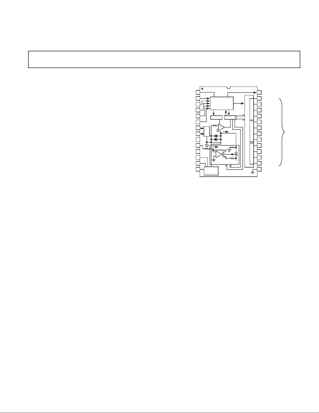
A/D Converters
*
AD674B
FUNCTIONAL BLOCK DIAGRAM
1
2
3
CS
4
0
5
6
CE
7
CC
8
9
AC
10
11
EE
12
13
IN
14
IN
10V
REF
199.95
k
VO LTAG E
DIVIDER
CONTROL
CLOCK SAR
COMP
–
+
I DAC
I REF
+
–
DAC
N
AD674B/AD774B
V
EE
/AD774B
MSB
N
Y
B
3
B
L
S
E
T
A
12
A
T
E
N
Y
O
B
U
B
T
L
P
E
U
T
B
N
B
Y
U
B
F
B
F
L
E
E
R
S
C
LSB
STATUS
28
STS
27
DB11 (MSB)
26
DB10
25
DB9
24
DB8
23
DB7
22
DB6
21
DB5
20
DB4
19
DB3
18
DB2
17
DB1
16
DB0 (LSB)
DIGITAL
15
COMMON DC
*
DIGITAL
DATA
OUTPUTS
PRODUCT DESCRIPTION
The AD674B and AD774B are complete 12-bit successiveapproximation analog-to-digital converters with three-state
output buffer circuitry for direct interface to 8- and 16-bit
microprocessor busses. A high-precision voltage reference and
clock are included on chip, and the circuit requires only power
supplies and control signals for operation.
The AD674B and AD774B are pin-compatible with the industry standard AD574A, but offer faster conversion time and busaccess speed than the AD574A and lower power consumption.
The AD674B converts in 15 µs (maximum) and the AD774B
converts in 8 µs (maximum).
The monolithic design is implemented using Analog Devices’
BiMOS II process allowing high-performance bipolar analog
circuitry to be combined on the same die with digital CMOS logic.
Offset, linearity, and scaling errors are minimized by active
laser trimming of thin-film resistors.
Five different grades are available. The J and K grades are
specified for operation over the 0°C to 70°C temperature range.
The A and B grades are specified from –40°C to +85°C, the T grade
is specified from –55°C to +125°C. The J and K grades are
available in a 28-lead plastic DIP or 28-lead SOIC. All other grades
are available in a 28-lead hermetically sealed ceramic DIP.
PRODUCT HIGHLIGHTS
1. Industry Standard Pinout: The AD674B and AD774B use
the pinout established by the industry standard AD574A.
2. Analog Operation: The precision, laser-trimmed scaling and
bipolar offset resistors provide four calibrated ranges: 0 V to
10 V and 0 V to 20 V unipolar; –5 V to +5 V and –10 V to
+10 V bipolar. The AD674B and AD774B operate on +5 V
and ± 12 V or ± 15 V power supplies.
3. Flexible Digital Interface: On-chip multiple-mode three-state
output buffers and interface logic allow direct connection to
most microprocessors. The 12 bits of output data can be
read either as one 12-bit word or as two 8-bit bytes (one with
8 data bits, the other with 4 data bits and 4 trailing zeros).
4. The internal reference is trimmed to 10.00 V with 1% maximum error and 10 ppm/°C typical temperature coefficient.
The reference is available externally and can drive up to
2.0 mA beyond the requirements of the converter and bipolar offset resistors.
5. The AD674B and AD774B are available in versions compliant with MIL-STD-883. Refer to the Analog Devices Military Products Databook or current AD674B/AD774B/883B
data sheet for detailed specifications.
*Protected by U.S. Patent Nos. 4,250,445; 4,808,908; RE30586.
REV. C
Information furnished by Analog Devices is believed to be accurate and
reliable. However, no responsibility is assumed by Analog Devices for its
use, nor for any infringements of patents or other rights of third parties that
may result from its use. No license is granted by implication or otherwise
under any patent or patent rights of Analog Devices.
One Technology Way, P.O. Box 9106, Norwood, MA 02062-9106, U.S.A.
Tel: 781/329-4700 www.analog.com
Fax: 781/326-8703 © Analog Devices, Inc., 2002
Page 2
(T
AD674B/AD774B–SPECIFICATIONS
V
= +5 V 10%, VEE = –15 V 10% or –12 V 5%, unless otherwise noted.)
LOGIC
MIN
to T
with VCC = +15 V 10% or +12 V 5%,
MAX
J Grade K Grade A Grade B Grade T Grade
Model (AD674B or AD774B) Min Typ Max Min Typ Max Min Typ Max Min Typ Max Min Typ Max Unit
RESOLUTION 12 12 12 12 12 Bits
LINEARITY ERROR @ 25°C 1 1/2 1 1/2 1/2 LSB
T
MIN
to T
MAX
1 1/2 1 1/2 1 LSB
DIFFERENTIAL LINEARITY ERROR
(Minimum Resolution for Which No
Missing Codes are Guaranteed) 12 12 12 12 12 Bits
UNIPOLAR OFFSET1 @ 25°C 2 2 2 2 2 LSB
BIPOLAR OFFSET1 @ 25°C 6 3 6 3 3 LSB
FULL-SCALE CALIBRATION ERROR
1, 2
@ 25°C (with Fixed 50 Ω Resistor
from REF OUT to REF IN) 0.1 0.25 0.1 0.125 0.1 0.25 0.1 0.125 0.1 0.125 % of FS
TEMPERATURE RANGE 0 70 0 70 –40 +85 –40 +85 –55 +125 °C
TEMPERATURE DRIFT
3
(Using Internal Reference)
Unipolar 2 1 2 1 1 LSB
Bipolar Offset 2 1 2 1 2 LSB
Full-Scale Calibration 6 2 8 5 7 LSB
POWER SUPPLY REJECTION
Max Change in Full-Scale Calibration
VCC = +15 V ± 1.5 V or +12 V ± 0.6 V 2 1 2 1 1 LSB
V
= +5 V ± 0.5 V 1/2 1/2 1/2 1/2 1/2 LSB
LOGIC
VEE = –15 V ± 1.5 V or –12 V ± 0.6 V 2 1 2 1 1 LSB
ANALOG INPUT
Input Ranges
Bipolar –5 +5 –5 +5 –5 +5 –5 +5 –5 +5 V
–10 +10 –10 +10 –10 +10 –10 +10 –10 +10 V
Unipolar 0 10 0 10 0 10 0 10 0 10 V
0 20 0 20 0 20 0 20 0 20 V
Input Impedance
10 V Span 3 5 735 735 735 735 7 kΩ
20 V Span 6 10 14 6 10 14 6 10 14 6 10 14 6 10 14 kΩ
POWER SUPPLIES
Operating Range
V
V
V
LOGIC
CC
EE
4.5 5.5 4.5 5.5 4.5 5.5 4.5 5.5 4.5 5.5 V
11.4 16.5 11.4 16.5 11.4 16.5 11.4 16.5 11.4 16.5 V
–16.5 –11.4 –16.5 –11.4 –16.5 –11.4 –16.5 –11.4 –16.5 –11.4 V
Operating Current
I
LOGIC
I
CC
I
EE
3.5 7 3.5 7 3.5 7 3.5 7 3.5 7 mA
3.5 7 3.5 7 3.5 7 3.5 7 3.5 7 mA
10 14 10 14 10 14 10 14 10 14 mA
POWER CONSUMPTION 220 375 220 375 220 375 220 375 220 375 mW
175 175 175 175 175 mW
INTERNAL REFERENCE VOLTAGE 9.9 10.0 10.1 9.9 10.0 10.1 9.9 10.0 10.1 9.9 10.0 10.1 9.9 10.0 10.1 V
Output Current
(Available for External Loads) 2.0 2.0 2.0 2.0 2.0 mA
(External Load Should Not
Change During the Conversion)
NOTES
1
Adjustable to zero.
2
Includes internal voltage reference error.
3
Maximum change from 25°C value to the value at T
4
Tested with REF OUT tied to REF IN through 50 Ω resistor, VCC = +16.5 V, VEE = –16.5 V, V
5
Tested with REF OUT tied to REF IN through 50 Ω resistor, VCC = +12 V, VEE = –12 V, V
Specifications subject to change without notice.
Specifications shown in boldface are tested on all devices at final electrical test at T
max specifications are guaranteed, although only those shown in boldface are tested.
MIN
or T
MAX
.
, 25°C, and T
MIN
= +5.5 V, and outputs in high-Z mode.
LOGIC
= +5 V, and outputs in high-Z mode.
LOGIC
. Results from those tests are used to calculate outgoing quality levels. All min and
MAX
4
5
–2–
REV. C
Page 3
t
HEC
t
HSC
t
SSC
t
HRC
t
SRC
t
SAC
t
HAC
t
C
t
DSC
CE
CS
R/C
A
0
STS
DB11 – DB0
HIGH
IMPEDANCE
AD674B/AD774B
(For all grades T
DIGITAL SPECIFICATIONS
VEE = –15 V 10% or –12 V 5%, unless otherwise noted.)
Parameter Test Conditions Min Max Unit
LOGIC INPUTS
V
IH
V
IL
I
IH
I
IL
C
IN
High Level Input Voltage 2.0 V
Low Level Input Voltage –0.5 +0.8 V
High Level Input Current VIN = V
Low Level Input Current VIN = 0 V –10 +10 µA
Input Capacitance 10 pF
LOGIC OUTPUTS
V
OH
V
OL
I
OZ
C
OZ
High Level Output Voltage IOH = 0.5 mA 2.4 V
Low Level Output Voltage IOL = 1.6 mA 0.4 V
High-Z Leakage Current VIN = 0 to V
High-Z Output Capacitance 10 pF
(For all grades T
SWITCHING SPECIFICATIONS
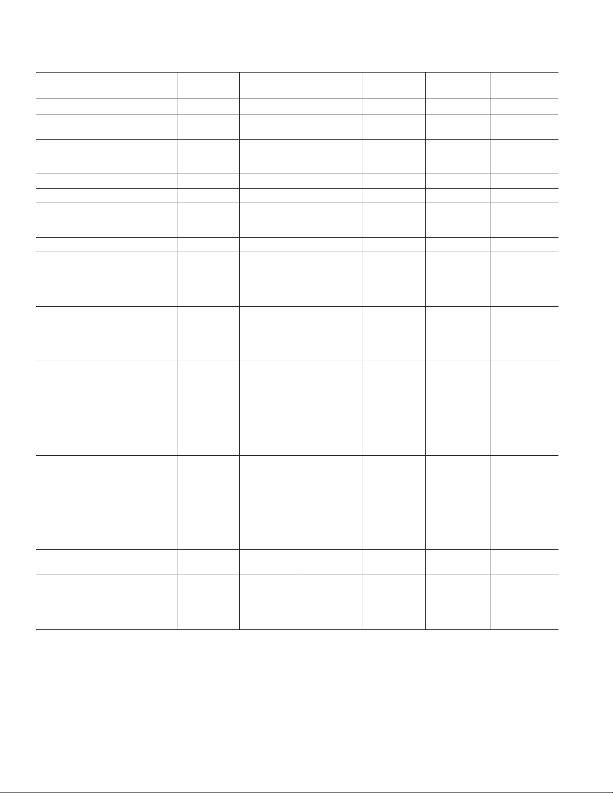
CONVERTER START TIMING (Figure 1)
J, K, A, B Grades T Grade
Parameter Symbol Min Typ Max Min Typ Max Unit
Conversion Time
8-Bit Cycle (AD674B) t
12-Bit Cycle (AD674B) t
8-Bit Cycle (AD774B) t
12-Bit Cycle (AD774B) t
STS Delay from CE t
CE Pulsewidth t
CS to CE Setup t
CS Low During CE High t
R/C to CE Setup t
R/C LOW During CE High t
A0 to CE Setup t
A0 Valid During CE High t
C
C
C
C
DSC
HEC
SSC
HSC
SRC
HRC
SAC
HAC
READ TIMING—FULL CONTROL MODE (Figure 2)
Parameter Symbol Min Typ Max Min Typ Max Unit
Access Time
CL = 100 pF t
Data Valid After CE Low t
Output Float Delay t
CS to CE Setup t
R/C to CE Setup t
A0 to CE Setup t
CS Valid After CE Low t
R/C High After CE Low t
A0 Valid After CE Low t
NOTES
1
tDD is measured with the load circuit of Figure 3a and is defined as the time required
for an output to cross 0.4 V or 2.4 V.
2
0°C to T
3
At –40°C.
4
At –55°C.
5
tHL is defined as the time required for the data lines to change 0.5 V when loaded with
the circuit of Figure 3b.
Specifications shown in boldface are tested on all devices at final electrical test with
MAX
.
worst case supply voltages at T
to calculate outgoing quality levels. All min and max specifications are guaranteed,
although only those shown in boldface are tested.
Specifications subject to change without notice.
REV. C
DD
HD
HL
SSR
SRR
SAR
HSR
HRR
HAR
MIN
6810 6810 µs
91215 91215 µs
456 456 µs
6 7.3 8 6 7.3 8 µs
50 50 ns
50 50 ns
50 50 ns
50 50 ns
50 50 ns
00ns
50 50 ns
J, K, A, B Grades T Grade
1
5
25
20
2
3
50 50 ns
00ns
50 50 ns
00ns
00ns
50 50 ns
, 25°C, and T
V
LOGIC
200 225 ns
75 150 75 150 ns
150 150 ns
. Results from those tests are used
MAX
to T
MIN
with VCC = +15 V 10% or +12 V 5%, V
MAX
LOGIC
to T
MIN
LOGIC
with VCC = +15 V 10% or +12 V 5%,
MAX
–10 +10 µA
–10 +10 µA
LOGIC
+ 0.5 V
LOGIC
= +5 V 10%, VEE = –15 V 10% or –12 V 5%, unless otherwise noted.)
Figure 1. Convert Start Timing
CE
t
HSR
t
HAR
t
HD
DATA
VA LI D
t
DD
25
15
t
CS
R/C
A
0
2
4
ns
ns
STS
DB11 – DB0
SSR
t
SRR
t
HIGH
IMPEDANCE
SAR
Figure 2. Read Cycle Timing
DB
N
3k
100pF
DB
N
HIGH-Z TO LOGIC 0HIGH-Z TO LOGIC 1
High-Z to Logic 1 High-Z to Logic 0
Figure 3a. Load Circuit for Access Time Test
DB
N
3k
LOGIC 1 TO HIGH-Z
100pF
DB
N
LOGIC 0 TO HIGH-Z
Logic 1 to High-Z Logic 0 to High-Z
Figure 3b. Load Circuit for Output Float Delay Test
–3–
= +5 V 10%,
t
HRR
HIGH
IMPEDANCE
t
HL
5V
3k
100pF
5V
3k
100pF
Page 4
AD674B/AD774B
WARNING!
ESD SENSITIVE DEVICE
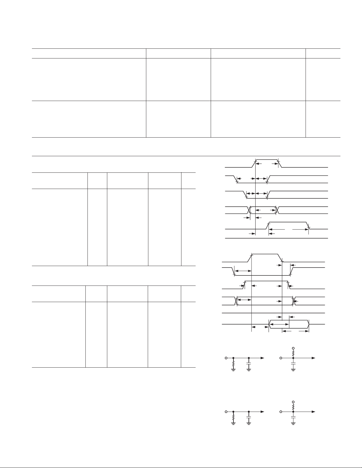
TIMING—STAND ALONE MODE (Figures 4a and 4b)
Parameter Symbol Min Typ Max Min Typ Max Unit
Data Access Time t
Low R/C Pulsewidth t
STS Delay from R/C t
Data Valid After R/C Low t
STS Delay After Data Valid t
High R/C Pulsewidth t
Specifications subject to change without notice.
J, K, A, B Grades T Grade
DDR
HRL
DS
HDR
HS
HRH
50 50 ns
25 25 ns
30 200 600 30 200 600 ns
150 150 ns
150 150 ns
200 225 ns
ABSOLUTE MAXIMUM RATINGS*
VCC to Digital Common . . . . . . . . . . . . . . . . . . . 0 to +16.5 V
to Digital Common . . . . . . . . . . . . . . . . . . . . 0 to –16.5 V
V
EE
V
to Digital Common . . . . . . . . . . . . . . . . . . . 0 to +7 V
LOGIC
Analog Common to Digital Common . . . . . . . . . . . . . . . ± 1 V
Digital Inputs to Digital Common . . . –0.5 V to V
Analog Inputs to Analog Common . . . . . . . . . . . . V
LOGIC
EE
+0.5 V
to V
CC
20 VIN to Analog Common . . . . . . . . . . . . . . . . . . . . . . ±24 V
REF OUT . . . . . . . . . . . . . . . . . . Indefinite Short to Common
. . . . . . . . . . . . . . . . . . . . . . . . . . . . . Momentary Short to V
CC
Junction Temperature . . . . . . . . . . . . . . . . . . . . . . . . . . 175°C
Power Dissipation . . . . . . . . . . . . . . . . . . . . . . . . . . . 825 mW
Lead Temperature, Soldering (10 sec) . . . . . . . . . . . . . 300°C
Storage Temperature . . . . . . . . . . . . . . . . . . –65°C to +150°C
*Stresses above those listed under Absolute Maximum Ratings may cause perma-
nent damage to the device. This is a stress rating only and functional operation of
the device at these or any other conditions above those indicated in the operational
section of this specification is not implied. Exposure to absolute maximum rating
conditions for extended periods may affect device reliability.
t
HRL
R/C
t
DS
STS
t
C
t
HDR
DB11–DB0
DATA
VA LI D
HIGH–Z
DATA VAL ID
Flgure 4a. Standalone Mode Timing Low Pulse R/
R/C
STS
DB11–DB0
t
HRH
t
DDRtHDR
HIGH–Z HIGH–Z
DATA
VA LI D
t
DS
t
C
t
HL
Figure 4b. Standalone Mode Timing High Pulse for R/
t
HS
C
C
ORDERING GUIDE
Conversion INL Package Package
MIN
to T
) Description Option
MAX
Model
l
Temperature Time (max) (T
AD674BJN 0°C to 70°C 15 µs ± 1 LSB Plastic DIP N-28
AD674BKN 0°C to 70°C 15 µs ± 1/2 LSB Plastic DIP N-28
AD674BAR –40°C to +85°C 15 µs ± 1 LSB Plastic SOIC R-28
AD674BBR –40°C to +85°C 15 µs ± 1/2 LSB Plastic SOIC R-28
AD674BAD –40°C to +85°C 15 µs ± 1 LSB Ceramic DIP D-28
AD674BBD –40°C to +85°C 15 µs ± 1/2 LSB Ceramic DIP D-28
AD674BTD –55°C to +125°C 15 µs ±1 LSB Ceramic DIP D-28
AD774BJN 0°C to 70°C8 µs ±1 LSB Plastic DIP N-28
AD774BKN 0°C to 70°C8 µs ± 1/2 LSB Plastic DIP N-28
AD774BAR –40°C to +85°C8 µs ±1 LSB Plastic SOIC R-28
AD774BBR –40°C to +85°C8 µs ± 1/2 LSB Plastic SOIC R-28
AD774BAD –40°C to +85°C8 µs ± 1 LSB Ceramic DIP D-28
AD774BBD –40°C to +85°C8 µs ± 1/2 LSB Ceramic DIP D-28
AD774BTD –55°C to +125°C8 µs ± 1 LSB Ceramic DIP D-28
NOTES
1
For details on grade and package offerings screened in accordance with MIL-STD-883, refer to the Analog Devices Military
Products Databook or the current AD674B/ AD774B/883B data sheet.
2
N = Plastic DIP; D = Hermetic DIP; R = Plastic SOIC.
CAUTION
ESD (electrostatic discharge) sensitive device. Electrostatic charges as high as 4000 V readily
accumulate on the human body and test equipment and can discharge without detection. Although
the AD674B/AD774B features proprietary ESD protection circuitry, permanent damage may occur
on devices subjected to high energy electrostatic discharges. Therefore, proper ESD precautions are
recommended to avoid performance degradation or loss of functionality.
2
REV. C–4–
Page 5

AD674B/AD774B
DEFINITION OF SPECIFICATIONS
Linearity Error
Linearity error refers to the deviation of each individual code
from a line drawn from “zero” through “full scale.” The point
used as “zero” occurs 1/2 LSB (1.22 mV for 10 V span) before
the first code transition (all zeroes to only the LSB “on”). “Full
scale” is defined as a level 1 1/2 LSB beyond the last code transition (to all ones). The deviation of a code from the true straight
line is measured from the middle of each particular code.
The K, B, and T grades are guaranteed for maximum nonlinearity of ± 1/2 LSB. For these grades, this means that an analog
value that falls exactly in the center of a given code width will
result in the correct digital output code. Values nearer the upper
or lower transition of the code width may produce the next upper
or lower digital output code. The J and A grades are guaranteed
to ± 1 LSB max error. For these grades, an analog value that
falls within a given code width will result in either the correct
code for that region or either adjacent one.
Note that the linearity error is not user adjustable.
Differential Linearity Error (No Missing Codes)
A specification that guarantees no missing codes requires that
every code combination appear in a monotonic increasing sequence
as the analog input level is increased. Thus every code must have a
finite width. The AD674B and AD774B guarantee no missing codes
to 12-bit resolution, requiring that all 4096 codes must be present
over the entire operating temperature ranges.
Unipolar Offset
The first transition should occur at a level 1/2 LSB above analog
common. Unipolar offset is defined as the deviation of the actual
transition from that point. This offset can be adjusted as discussed
later. The unipolar offset temperature coefficient specifies the
maximum change of the transition point over temperature,
with or without external adjustment.
Bipolar Offset
In the bipolar mode the major carry transition (0111 1111 1111
to 1000 0000 0000) should occur for an analog value 1/2 LSB
below analog common. The bipolar offset error and temperature
coefficient specify the initial deviation and maximum change in
the error over temperature.
Quantization Uncertainty
Analog-to-digital converters exhibit an inherent quantization
uncertainty of ±1/2 LSB. This uncertainty is a fundamental
characteristic of the quantization process and cannot be reduced
for a converter of given resolution.
Left-Justified Data
The output data format is left-justified. This means that the
data represents the analog input as a fraction of full scale, ranging from 0 to 4095/4096. This implies a binary point 4095 to
the left of the MSB.
Full-Scale Calibration Error
The last transition (from 1111 1111 1110 to 1111 1111 1111)
should occur for an analog value 1 1/2 LSB below the nominal
full scale (9.9963 V for 10.000 V full scale). The full-scale calibration error is the deviation of the actual level at the last transition from the ideal level. This error, which is typically 0.05% to
0.1% of full scale, can be trimmed out as shown in Figures 7
and 8. The full-scale calibration error over temperature is given
with and without the initial error trimmed out. The temperature
coefficients for each grade indicate the maximum change in the
full-scale gain from the initial value using the internal 10 V
reference.
Temperature Drift
The temperature drift for full-scale calibration, unipolar offset,
and bipolar offset specifies the maximum change from the initial
(25°C) value to the value at T
Power Supply Rejection
MIN
or T
MAX
.
The standard specifications assume use of +5.00 V and ±15.00 V
or ± 12.00 V supplies. The only effect of power supply error on
the performance of the device will be a small change in the
full-scale calibration. This will result in a linear change in all
low-order codes. The specifications show the maximum fullscale change from the initial value with the supplies at the
various limits.
Code Width
A fundamental quantity for A/D converter specifications is the
code width. This is defined as the range of analog input values for
which a given digital output code will occur. The nominal value
of a code width is equivalent to 1 least significant bit (LSB) of the
full-scale range or 2.44 mV out of 10 V for a 12-bit ADC.
REV. C
–5–
Page 6

AD674B/AD774B
PIN CONFIGURATION
1
V
LOGIC
2
12/8
3
CS
4
A
0
AD674B
5
R/C
CE
V
REF OUT
AGND
REF IN
V
BIP OFF
10 V
20 V
CC
EE
IN
IN
6
AD774B
7
TOP VIEW
(Not to Scale)
8
9
10
11
12
13
14
OR
PIN FUNCTION DESCRIPTIONS
Symbol Pin No. Type* Name and Function
AGND 9 P Analog Ground (Common)
A
0
4 DI Byte Address/Short Cycle. If a conversion is started with A0 Active LOW, a full 12-bit conversion
cycle is initiated. If A
is Active HIGH during a convert start, a shorter 8-bit conversion cycle
0
results. During Read (R/C = 1) with 12/8 LOW, A
= HIGH enables DB3–DB0 and sets DB7–DB4 = 0.
and A
0
BIP OFF 12 AI Bipolar Offset. Connect through a 50 Ω resistor to REF OUT for bipolar operation or to Analog
Common for unipolar operation.
CE 6 DI Chip Enable. Chip Enable is Active HIGH and is used to initiate a convert or read operation.
CS 3 DI Chip Select. Chip Select is Active LOW.
DB11–DB8 27–24 DO Data Bits 11 through 8. In the 12-bit format (see 12/8 and A
4 bits of data. In the 8-bit format, they provide the upper 4 bits when A
disabled when A
is HIGH.
0
DB7–DB4 23–20 DO Data Bits 7 through 4. In the 12-bit format these pins provide the middle 4 bits of data. In the
8-bit format they provide the middle 4 bits when A
DB3–DB0 19–16 DO Data Bits 3 through 0. In both the 12-bit and 8-bit format these pins provide the lower 4 bits of
data when A
is HIGH; they are disabled when A0 is LOW.
0
DGND 15 P Digital Ground (Common)
REF OUT 8 AO 10 V Reference Output
R/C 5 DI Read/Convert. In the full control mode R/C is Active HIGH for a read operation and Active LOW
for a convert operation. In the standalone mode, the falling edge of R/C initiates a conversion.
REF IN 10 AI Reference Input is connected through a 50 Ω resistor to +10 V Reference for normal operation.
STS 28 DO Status is Active HIGH when a conversion is in progress and goes LOW when the conversion is
completed.
V
CC
V
EE
V
LOGIC
10 V
20 V
IN
IN
7 P +12 V/+15 V Analog Supply
11 P –12 V/–15 V Analog Supply
1 P 5 V Logic Supply
13 AI 10 V Span Input, 0 V to +10 V unipolar mode or –5 V to +5 V bipolar mode. When using the
20 V Span, 10 V
should not be connected.
IN
14 AI 20 V Span Input, 0 V to +20 V unipolar mode or –10 V to +10 V bipolar mode. When using the
10 V Span, 20 V
should not be connected.
IN
12/8 2 DI The 12/8 pin determines whether the digital output data is to be organized as two 8-bit words
(12/8 LOW) or a single 12-bit word (12/8 HIGH).
*Types: AI = Analog Input, AO = Analog Output, DI = Digital Input, DO = Digital Output, P = Power
STS
28
DB11 (MSB)
27
DB10
26
25
DB9
24
DB8
23
DB7
22
DB6
21
DB5
20
DB4
19
DB3
18
DB2
17
DB1
16
DB0 (LSB)
15
DGND
= LOW enables the 8 most significant bits,
0
pins) these pins provide the upper
0
is LOW and are
0
is LOW and all zeroes when A0 is HIGH.
0
REV. C–6–
Page 7

AD674B/AD774B
CIRCUIT OPERATION
The AD674B and AD774B are complete 12-bit monolithic A/D
converters that require no external components to provide the
complete successive-approximation analog-to-digital conversion
function. A block diagram is shown in Figure 5.
5V SUPPLY
V
DATA MODE SELECT
READ/CONVERT R/C
ANALOG COMMON
REFERENCE INPUT
LOGIC
12/8
CHIP SELECT
BYTE ADDRESS/
SHORT CYCLE A
CHIP ENABLE
12V/15V SUPPLY
10V REFERENCE
–12V/–15V SUPPLY
BIPOLAR OFFSET
V
REF OUT
REF IN
V
BIPOFF
10V SPAN INPUT
10V
20V SPAN INPUT
20V
1
2
3
CS
4
0
5
6
CE
7
CC
8
9
AC
10
11
EE
12
13
IN
14
IN
REF
199.95
k
10V
VO LTAG E
DIVIDER
CONTROL
CLOCK SAR
COMP
–
+
I DAC
I REF
+
–
DAC
N
AD674B/AD774B
MSB
3
S
T
A
12
T
E
O
U
T
P
U
T
B
U
F
F
E
R
S
V
EE
LSB
N
Y
B
B
L
E
A
N
Y
B
B
L
E
B
N
Y
B
B
L
E
C
STATUS
28
STS
27
DB11 (MSB)
26
DB10
25
DB9
24
DB8
23
DB7
22
DB6
21
DB5
20
DB4
19
DB3
18
DB2
17
DB1
16
DB0 (LSB)
DIGITAL
15
COMMON DC
DIGITAL
DATA
OUTPUTS
Figure 5. Block Diagram of AD674B and AD774B
When the control section is commanded to initiate a conversion
(as described later) it enables the clock and resets the
successive-approximation register (SAR) to all zeroes. Once a
conversion cycle has begun, it cannot be stopped or restarted
and data is not available from the output buffers. The SAR,
timed by the clock, will sequence through the conversion cycle
and return an end-of-convert flag to the control section. The
control section will then disable the clock, bring the output
status flag low, and enable control functions to allow data read
by external command.
During the conversion cycle, the internal 12-bit current output
DAC is sequenced by the SAR from the most significant bit
(MSB) to least significant bit (LSB) to provide an output current that accurately balances the input signal current through
the divider network. The comparator determines whether the
addition of each successively weighted bit current causes the
DAC current sum to be greater or less than the input current; if
the sum is less, the bit is left on; if more, the bit is turned off.
After testing all the bits, the SAR contains a 12-bit binary code
that accurately represents the input signal to within ±1/2 LSB.
The temperature-compensated reference provides the primary
voltage reference to the DAC and guarantees excellent stability
with both time and temperature. The reference is trimmed to
10.00 V ± 1%; it can supply up to 2.0 mA to an external load in
addition to the requirements of the reference input resistor
(0.5 mA) and bipolar offset resistor (0.5 mA). Any external load
on the reference must remain constant during conversion. The
thin-film application resistors are trimmed to match the fullscale output current of the DAC. The input divider network
provides a 10 V or 20 V input range. The bipolar offset resistor
is grounded for unipolar operation and connected to the 10 V
reference for bipolar operation.
DRIVING THE ANALOG INPUT
The AD674B and AD774B are successive-approximation analogto-digital converters. During the conversion cycle, the ADC input
current is modulated by the DAC test current at approximately
a 1 MHz rate. Thus it is important to recognize that the signal
source driving the ADC must be capable of holding a constant
output voltage under dynamically changing load conditions.
FEEDBACK TO AMPLIFIER
V+
R
IN
ADC
I
IN
CURRENT
OUTPUT
I
TEST
COMPARATOR
DAC
SAR
CURRENT
LIMITING
RESISTORS
ANALOG COMMON
I
IS MODULATED BY
IN
CHANGES IN TEST CURRENT.
AMPLIFIER PULSE LOAD
RESPONSE LIMITED BY
OPEN-LOOP OUTPUT IMPEDANCE.
V–
I
DIFF
Figure 6. Op Amp—ADC Interface
The closed-loop output impedance of an op amp is equal to the
open-loop output impedance (usually a few hundred ohms)
divided by the loop gain at the frequency of interest. It is often
assumed that the loop gain of a follower-connected op amp is
sufficiently high to reduce the closed-loop output impedance to
a negligibly small value, particularly if the signal is low frequency. However, the amplifier driving the ADC must either
have sufficient loop gain at 1 MHz to reduce the closed-loop
output impedance to a low value or have low open-loop output
impedance. This can be accomplished by using a wideband op
amp, such as the AD711.
If a sample-hold amplifier is required, the monolithic AD585 or
AD781 is recommended, with the output buffer driving the
AD674B or AD774B input directly. A better alternative is the
AD1674, which is a 10 µs sampling ADC in the same pinout as the
AD574A, AD674A, or AD774B and is functionally equivalent.
SUPPLY DECOUPLING AND LAYOUT
CONSIDERATION
It is critical that the power supplies be filtered, well regulated,
and free from high-frequency noise. Use of noisy supplies will
cause unstable output codes. Switching power supplies is not
recommended for circuits attempting to achieve 12-bit accuracy
unless great care is used in filtering any switching spikes present
in the output. Few millivolts of noise represent several counts of
error in a 12-bit ADC.
Decoupling capacitors should be used on all power supply pins;
the 5 V supply decoupling capacitor should be connected directly
from Pin 1 to Pin 15 (digital common) and the +V
and –V
CC
EE
pins should be decoupled directly to analog common (Pin 9). A
suitable decoupling capacitor is a 4.7 µF tantalum type in paral-
lel with a 0.1 µF ceramic disc type.
REV. C
–7–
Page 8

AD674B/AD774B
Circuit layout should attempt to locate the ADC, associated
analog input circuitry, and interconnections as far as possible
from logic circuitry. For this reason, the use of wire-wrap circuit
construction is not recommended. Careful printed-circuit layout
and manufacturing is preferred.
UNIPOLAR RANGE CONNECTIONS FOR THE AD674B AND AD774B
The AD674B and AD774B contain all the active components
required to perform a complete 12-bit A/D conversion. Thus,
for most situations, all that is necessary is connection of the
power supplies (+5 V, +12/+15 V, and –12/–15 V), the analog
input, and the conversion initiation command, as discussed on
the next page.
AD674B/AD774B
2
12/8
3
CS
4
A
0
5
R/C
CE
6
REF IN
10
REF OUT
8
BIP OFF
12
10V
13
IN
20V
14
IN
ANA COM
9
STS 28
HIGH BITS
24–27
MIDDLE BITS
20–23
LOW BITS
16–19
+5V 1
+15V 7
–15V 11
DIG COM 15
–12V/
–15V
100k
ANALOG
OFFSET
100k
100
0 TO 10V
INPUTS
0 TO 20V
R1
+12V/
+15V
GAIN
R2
100
Figure 7. Unipolar Input Connections
UNIPOLAR CALIBRATION
The connections for unipolar ranges are shown in Figure 7. The
AD674B or AD774B is trimmed to a nominal 1/2 LSB offset so
that the exact analog input for a given code will be in the middle
of that code (halfway between the transitions to the codes above
and below it). Thus, when properly calibrated, the first transition
(from 0000 0000 0000 to 0000 0000 0001) will occur for an input
level of +1/2 LSB (1.22 mV for 10 V range).
If Pin 12 is connected to Pin 9, the unit will behave in this manner,
within specifications. If the offset trim (R1) is used, it should be
trimmed as above, although a different offset can be set for a
particular system requirement. This circuit will give approximately
± 15 mV of offset trim range.
The full-scale trim is done by applying a signal 1 1/2 LSB below
the nominal full scale (9.9963 for a 10 V range). Trim R2 to
give the last transition (1111 1111 1110 to 1111 1111 1111).
BIPOLAR OPERATION
The connections for bipolar ranges are shown in Figure 8.
Again, as for the unipolar ranges, if the offset and gain specifications are sufficient, one or both of the trimmers shown can be
replaced by a 50 Ω ± 1% fixed resistor. The analog input is
applied as for the unipolar ranges. Bipolar calibration is similar
to unipolar calibration. First, a signal 1/2 LSB above negative
full scale (–4.9988 V for the ±5 V range) is applied and R1 is
trimmed to give the first transition (0000 0000 0000 to 0000
0000 0001). Then a signal 1 1/2 LSB below positive full scale
(+4.9963 V for the ±5 V range) is applied and R2 trimmed to
give the last transition (1111 1111 1110 to 1111 1111 1111).
All of the thin-film application resistors of the AD674B and
AD774B are factory trimmed for absolute calibration. Therefore,
in many applications, no calibration trimming will be required.
The absolute accuracy for each grade is given in the specification
tables. For example, if no trims are used, ±2 LSB max zero offset
error and ± 0.25% (10 LSB) max full-scale error are guaranteed.
If the offset trim is not required, Pin 12 can be connected directly
to Pin 9; the two resistors and trimmer for Pin 12 are then not
needed. If the full-scale trim is not required, a 50 Ω 1% metal
film resistor should be connected between Pin 8 and Pin 10.
The analog input is connected between Pins 13 and 9 for a 0 V
to 10 V input range, between Pins 14 and 9 for a 0 V to 20 V
input range. Input signals beyond the supplies are easily accommodated. For the 10 V span input, the LSB has a nominal value of
2.44 mV; for the 20 V span, 4.88 mV. If a 10.24 V range is
desired (nominal 2.5 mV/bit), the gain trimmer (R2) should be
replaced by a 50 Ω resistor and a 200 Ω trimmer inserted in
series with the analog input to Pin 13 (for a full-scale range of
20.48 V [5 mV/bit] use a 500 Ω trimmer into Pin 14). The
gain trim described below is now done with these trimmers.
The nominal input impedance into Pin 13 is 5 kΩ, and into Pin
14 is 10 kΩ.
AD674B/AD774B
GAIN
OFFSET
ANALOG
INPUTS
5V
10V
R2
R1
100
100
2
12/8
3
CS
4
A
5
R/C
CE
6
REF IN
10
REF OUT
8
BIP OFF
12
10V
13
20V
14
ANA COM
9
0
IN
IN
STS 28
HIGH BITS
24–27
MIDDLE BITS
20–23
LOW BITS
16–19
+5V 1
+15V 7
–15V 11
DIG COM 15
Figure 8. Bipolar Input Connections
GROUNDING CONSIDERATIONS
The analog common at Pin 9 is the ground reference point for
the internal reference and is thus the “high quality” ground for
the ADC; it should be connected directly to the analog reference
point of the system. To achieve the high-accuracy performance
available from the ADC in an environment of high digital noise
content, the analog and digital commons must be connected
together at the package. In some situations, the digital common
at Pin 15 can be connected to the most convenient ground reference point; digital power return is preferred.
REV. C–8–
Page 9

AD674B/AD774B
VALUE OF A0 AT LAST CONVERT COMMAND
CE
CS
R/C
12/8
D
EN
R
Q
S
A
0
READ
Q
D
EN
START CONVERT
S
Q
R
QB
HIGH IF CONVERSION
IN PROGRESS
CLK EN
STATUS
NYBBLE A
ENABLE
NYBBLE B
ENABLE
NYBBLE C
ENABLE
NYBBLE = 0
ENABLE
EOC 12
EOC 8
SAR
RESET
TO
OUTPUT
BUFFERS
Figure 9. Equivalent Internal Logic Circuitry
CONTROL LOGIC
The AD674B and AD774B contain on-chip logic to provide
conversion initiation and data read operations from signals
commonly available in microprocessor systems; this internal
logic circuitry is shown in Figure 9.
The control signals CE, CS, and R/C control the operation of
the converter. The state of R/C when CE and CS are both
asserted determines whether a data read (R/C = 1) or a convert
(R/C = 0) is in progress. The register control inputs, A
and
0
12/8, control conversion length and data format. If a conversion
is started with A
If A
is high during a convert start, a shorter 8-bit conversion
0
cycle results. During data read operations, A
low, a full 12-bit conversion cycle is initiated.
0
determines
0
whether the three-state buffers containing the 8 MSBs of the
conversion result (A
= 0) or the 4 LSBs (A0 = 1) are enabled.
0
The 12/8 pin determines whether the output data is to be organized as two 8-bit words (12/8 tied to DIGITAL COMMON)
or a single 12-bit word (12/8 tied to V
the byte addressed when A
is high contains the 4 LSBs from
0
). In the 8-bit mode,
LOGIC
the conversion followed by four trailing zeroes. This organization allows the data lines to be overlapped for direct interface to
8-bit buses without the need for external three-state buffers.
An output signal, STS, indicates the status of the converter.
STS goes high at the beginning of a conversion and returns low
when the conversion cycle is complete.
Table I. Truth Table
CE CS R/C 12/8 A0 Operation
0XXXXNone
X1 XXXNone
1 0 0 X 0 Initiate 12-Bit Conversion
1 0 0 X 1 Initiate 8-Bit Conversion
1011XEnable 12-Bit Parallel Output
10100Enable 8 Most Significant Bits
10101Enable 4 LSBs + 4 Trailing Zeroes
The ADC may be operated in one of two modes, the full-control
mode and the standalone mode. The full-control mode uses all
the control signals and is useful in systems that address decode
multiple devices on a single data bus. The standalone mode is
useful in systems with dedicated input ports available. In general, the standalone mode is capable of issuing start-convert
commands on a more precise basis and therefore produces
higher accuracy results. The following sections describe these
two modes in more detail.
FULL-CONTROL MODE
Chip Enable (CE), Chip Select (CS), and Read/Convert (R/C)
are used to control Convert or Read modes of operation. Either
CE or CS may be used to initiate a conversion. The state of R/C
when CE and CS are both asserted determines whether a data
Read (R/C = 1) or a Convert (R/C = 0) is in progress. R/C
should be LOW before both CE and CS are asserted; if R/C is
HIGH, a Read operation will momentarily occur, possibly
resulting in system bus contention.
REV. C
–9–
Page 10

AD674B/AD774B
STANDALONE MODE
“Standalone” mode is useful in systems with dedicated input
ports available and thus not requiring full bus interface capability. Standalone mode applications are generally able to issue
conversion start commands more precisely than full-control
mode, resulting in improved accuracy.
CE and 12/8 are wired HIGH, CS and A
are wired LOW, and
0
conversion is controlled by R/C. The three-state buffers are
enabled when R/C is HIGH and a conversion starts when R/C
goes LOW. This gives rise to two possible control signals—a
high pulse or a low pulse. Operation with a low pulse is shown
in Figure 4a. In this case, the outputs are forced into the high
impedance state in response to the falling edge of R/C and
return to valid logic levels after the conversion cycle is completed.
The STS line goes HIGH 200 ns after R/C goes LOW and
returns low 600 ns after data is valid.
If conversion is initiated by a high pulse as shown in Figure 4b,
the data lines are enabled during the time when R/C is HIGH.
The falling edge of R/C starts the next conversion, and the data
lines return to three-state (and remain three-state) until the next
high pulse of R/C.
CONVERSION TIMING
Once a conversion is started, the STS line goes HIGH. Convert
start commands will be ignored until the conversion cycle is
complete. The output data buffers can be enabled up to 1.2 µs
prior to STS going LOW. The STS line will return LOW at the
end of the conversion cycle.
The register control inputs, A
length and data format. If a conversion is started with A
a full 12-bit conversion cycle is initiated. If A
and 12/8, control conversion
0
is HIGH during a
0
LOW,
0
convert start, a shorter 8-bit conversion cycle results.
During data read operations, A
determines whether the three-
0
state buffers containing the 8 MSBs of the conversion result
= 0) or the 4 LSBs (A0 = 1) are enabled. The 12/8 pin
(A
0
determines whether the output data is to be organized as two
8-bit words (12/8 tied LOW) or a single 12-bit word (12/8 tied
HIGH). In the 8-bit mode, the byte addressed when A
is high
0
contains the 4 LSBs from the conversion followed by four trailing zeroes. This organization allows the data lines to be overlapped for direct interface to 8-bit buses without the need for
external three-state buffers.
GENERAL A/D CONVERTER INTERFACE
CONSIDERATIONS
A typical A/D converter interface routine involves several operations. First, a write to the ADC address initiates a conversion.
The processor must then wait for the conversion cycle to complete, since most integrated circuit ADCs take longer than one
instruction cycle to complete a conversion. Valid data can, of
course, only be read after the conversion is complete. The
AD674B and AD774B provide an output signal (STS) which
indicates when a conversion is in progress. This signal can be
polled by the processor by reading it through an external threestate buffer (or other input port). The STS signal can also
generate an interrupt upon completion of conversion if the system timing requirements are critical and the processor has other
tasks to perform during the ADC conversion cycle. Another
possible time-out method is to assume that the ADC will take its
maximum conversion time to convert, and insert a sufficient
number of “no-op” instructions to ensure that this amount of
processor time is consumed.
Once conversion is complete, the data can be read. For converters with more data bits than are available on the bus, a choice of
data formats is required, and multiple read operations are
needed. The AD674B and AD774B include internal logic to
permit direct interface to 8-bit and 16-bit data buses, selected
by the 12/8 input. In 16-bit bus applications (12/8 high) the
data lines (DB11 through DB0) may be connected to either the
12 most significant or 12 least significant bits of the data bus.
The remaining 4 bits should be masked in software. The interface to an 8-bit data bus (12/8 low) is done in a left-justified format. The even address (A
through DB4). The odd address (A
low) contains the 8 MSBs (DB11
0
high) contains the 4 LSBs
0
(DB3 through DB0) in the upper half of the byte, followed by
four trailing zeroes, thus eliminating bit masking instructions.
It is not possible to rearrange the output data lines for right-justified 8-bit bus interface.
D7 D0
DB11
XXX0
(EVEN ADDR)
XXX1
(ODD ADDR)
DB10 DB9 DB8 DB7 DB6 DB5 DB4
(MSB)
DB3 DB2 DB1
DB0
0000
(LSB)
Figure 10. Data Format for 8-Bit Bus
REV. C–10–
Page 11

0.085
0.0125 (0.32)
0.0091 (0.23)
8
0
0.0291 (0.74)
0.0098 (0.25)
45
0.0500 (1.27)
0.0157 (0.40)
SEATING
PLANE
0.0118 (0.30)
0.0040 (0.10)
0.0192 (0.49)
0.0138 (0.35)
0.1043 (2.65)
0.0926 (2.35)
0.0500
(1.27)
BSC
28 15
141
0.7125 (18.10)
0.6969 (17.70)
0.4193 (10.65)
0.3937 (10.00)
0.2992 (7.60)
0.2914 (7.40)
PIN 1
(2.16)
0.017 0.003
28
1
+
–
(0.43)
OUTLINE DIMENSIONS
Dimensions shown in inches and (mm).
28-Lead Ceramic DIP Package
(D-28)
0.050 (12.83)
15
0.59
+
0.01
–
(14.98)
1.42 (36.07)
1.40 (35.56)
0.1 (2.54)
+
0.047 0.007
–
(1.19)
14
0.095 (2.41)
0.050
+
0.010
–
(1.27)
SEATING
PLANE
28-Lead Plastic DIP Package
(N-28)
o
30
0.010 0.002
(0.254 0.05)
0.6 (15.24)
0.05 (1.27)
0.045 (1.14)
0.08 (2.0)
0.125 MIN (3.17)
0.145 0.02
(3.68)
+
–
+
–
AD674B/AD774B
+
–
PIN 1
0.250
(6.35)
MAX
0.200 (5.05)
0.125 (3.18)
1.565 (39.70)
1.380 (35.10)
28
15
0.580 (14.73)
0.485 (12.32)
114
0.022 (0.558)
0.014 (0.356)
0.100
(2.54)
BSC
0.060 (1.52)
0.015 (0.38)
0.070
(1.77)
MAX
SEATING
PLANE
0.150
(3.81)
MIN
0.625 (15.87)
0.600 (15.24)
28-Lead Wide Body SOIC Package
(R-28)
0.195 (4.95)
0.125 (3.18)
0.015 (0.381)
0.008 (0.204)
REV. C
–11–
Page 12

AD674B/AD774B
Revision History
Location Page
Data Sheet changed from REV. B to REV. C.
Edits to ORDERING GUIDE . . . . . . . . . . . . . . . . . . . . . . . . . . . . . . . . . . . . . . . . . . . . . . . . . . . . . . . . . . . . . . . . . . . . . . . . . . . . . . 5
Add 28-Lead Wide Body SOIC Package Drawing . . . . . . . . . . . . . . . . . . . . . . . . . . . . . . . . . . . . . . . . . . . . . . . . . . . . . . . . . . . . . . 12
C00808-0-4/02(C)
PRINTED IN U.S.A.
REV. C–12–
 Loading...