

Page 1
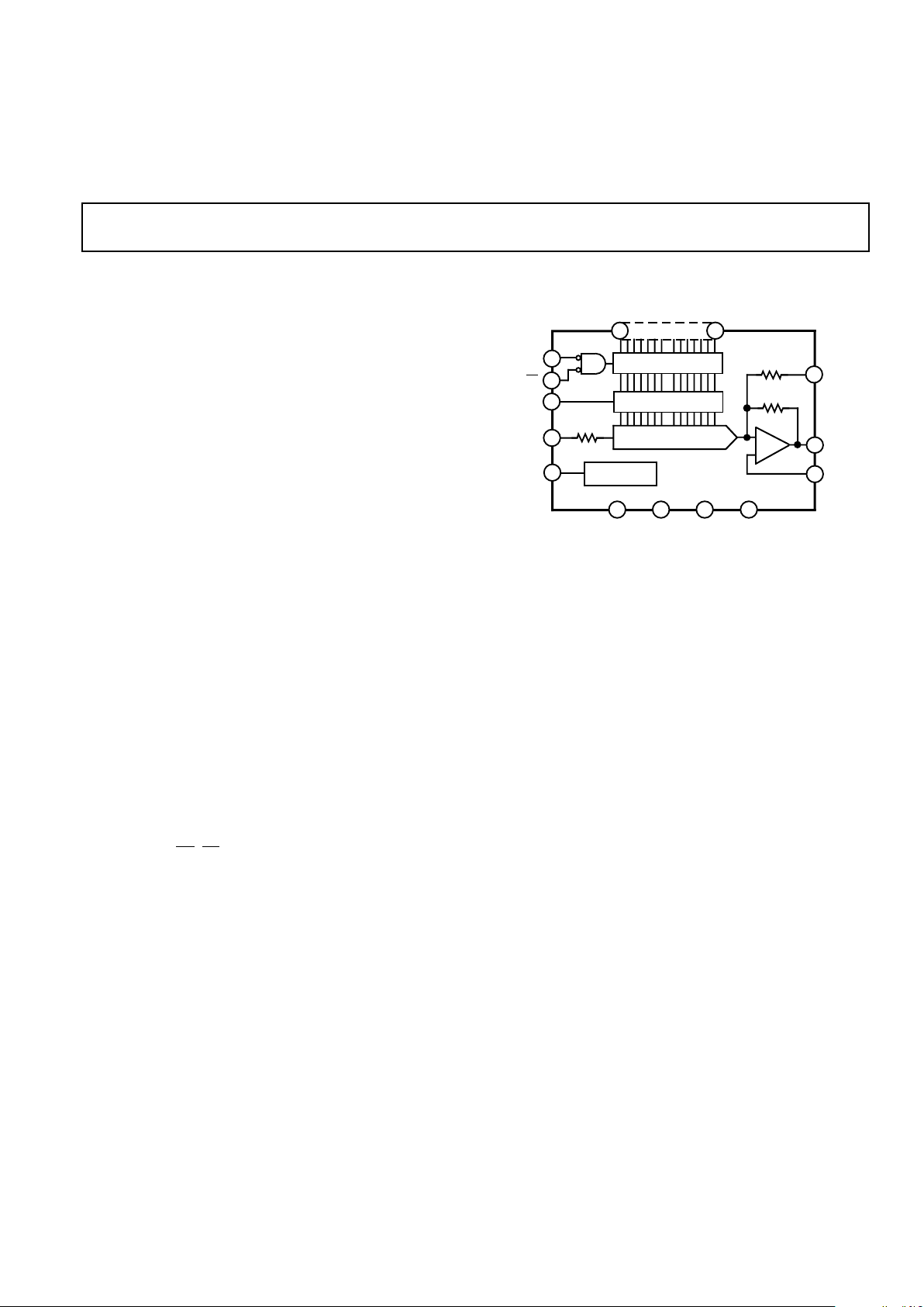
FUNCTIONAL BLOCK DIAGRAM
LDAC
SPAN/
BIP OFF
AGND
DB15
(MSB) (LSB)
DB0
DGND
CS
L1
REF IN
REF OUT
–V
EE
+V
CC
+V
LL
V
OUT
16-BIT LATCH
10k
AMP
AD669
227
6
5
23
27
28
10V REF
2143
26
24
10k
10.05k
16-BIT LATCH
16-BIT DAC
25
REV. A
Information furnished by Analog Devices is believed to be accurate and
reliable. However, no responsibility is assumed by Analog Devices for its
use, nor for any infringements of patents or other rights of third parties
which may result from its use. No license is granted by implication or
otherwise under any patent or patent rights of Analog Devices.
a
Monolithic 16-Bit
DACPORT
AD669
FEATURES
Complete 16-Bit D/A Function
On-Chip Output Amplifier
High Stability Buried Zener Reference
Monolithic BiMOS II Construction
61 LSB Integral Linearity Error
15-Bit Monotonic over Temperature
Microprocessor Compatible
16-Bit Parallel Input
Double-Buffered Latches
Fast 40 ns Write Pulse
Unipolar or Bipolar Output
Low Glitch: 15 nV-s
Low THD+N: 0.009%
MIL-STD-883 Compliant Versions Available
GENERAL DESCRIPTION
The AD669 DACPORT® is a complete 16-bit monolithic D/A
converter with an on-board reference and output amplifier. It is
manufactured on Analog Devices’ BiMOS II process. This process allows the fabrication of low power CMOS logic functions
on the same chip as high precision bipolar linear circuitry. The
AD669 chip includes current switches, decoding logic, an output
amplifier, a buried Zener reference and double-buffered latches.
The AD669’s architecture insures 15-bit monotonicity over
temperature. Integral nonlinearity is maintained at ± 0.003%,
while differential nonlinearity is ± 0.003% max. The on-chip
output amplifier provides a voltage output settling time of 10 µs
to within 1/2 LSB for a full-scale step.
Data is loaded into the AD669 in a parallel 16-bit format. The
double-buffered latch structure eliminates data skew errors and
provides for simultaneous updating of DACs in a multi-DAC
system. Three TTL/LSTTL/5 V CMOS compatible signals control the latches:
CS, L1 and LDAC.
The output range of the AD669 is pin programmable and can
be set to provide a unipolar output range of 0 V to +10 V or a
bipolar output range of –10 V to +10 V.
The AD669 is available in seven grades: AN and BN versions
are specified from –40°C to +85°C and are packaged in a 28-pin
plastic DIP. The AR and BR versions are specified for –40°C to
+85°C operation and are packaged in a 28-pin SOIC. The SQ
version is specified from –55°C to +125°C and is packaged in a
hermetic 28-pin cerdip package. The AD669 is also available
compliant to MIL-STD-883. Refer to the AD669/883B data
sheet for specifications and test conditions.
DACPORT is a registered trademark of Analog Devices, Inc.
One Technology Way, P.O. Box 9106, Norwood, MA 02062-9106, U.S.A.
Tel: 617/329-4700 Fax: 617/326-8703
PRODUCT HIGHLIGHTS
1. The AD669 is a complete voltage output 16-bit DAC with
voltage reference and digital latches on a single IC chip.
2. The internal buried Zener reference is laser trimmed to
10.000 volts with a ±0.2% maximum error. The reference
voltage is also available for external applications.
3. The AD669 is both dc and ac specified. DC specs include
±1 LSB INL error and ±1 LSB DNL error. AC specs include
0.009% THD+ N and 83 dB SNR. The ac specifications
make the AD669 suitable for signal generation applications.
4. The double-buffered latches on the AD669 eliminate data
skew errors while allowing simultaneous updating of DACs in
multi-DAC systems.
5. The output range is a pin-programmable unipolar 0 V to
+10 V or bipolar –10 V to +10 V output. No external components are necessary to set the desired output range.
6. The AD669 is available in versions compliant with MILSTD-883. Refer to the Analog Devices Military Products
Databook or current AD669/883B data sheet for detailed
specifications.
Page 2

AD669–SPECIFICATIONS
Model AD669AN/AR AD669AQ/SQ AD669BN/BQ/BR
Min Typ Max Min Typ Max Min Typ Max Units
RESOLUTION 16 16 16 Bits
DIGITAL INPUTS (T
MIN
to T
MAX
)
V
IH
(Logic “1” ) 2.0 5.5 * * * * Volts
V
IL
(Logic “0” ) 0 0.8 * * * * Volts
I
IH
(VIH = 5.5 V) 610 **µA
I
IL
(VIL = 0 V) 610 **µA
TRANSFER FUNCTION CHARACTERISTICS
1
Integral Nonlinearity 62 * 61 LSB
T
MIN
to T
MAX
64 * 62 LSB
Differential Nonlinearity 62 * 61 LSB
T
MIN
to T
MAX
64 * 62 LSB
Monotonicity Over Temperature 14 14 15 Bits
Gain Error
2, 5
60.15 60.10 60.10 % of FSR
Gain Drift
2
(T
MIN
to T
MAX
) 25 15 15 ppm/°C
Unipolar Offset 65 65 62.5 mV
Unipolar Offset Drift (T
MIN
to T
MAX
) 533ppm/°C
Bipolar Zero Error 615 615 610 mV
Bipolar Zero Error Drift (T
MIN
to T
MAX
) 12 10 5 ppm/°C
REFERENCE INPUT
Input Resistance 7 10 13 ****** kΩ
Bipolar Offset Input Resistance 7 10 13 ****** kΩ
REFERENCE OUTPUT
Voltage 9.98 10.00 10.02 ****** Volts
Drift 25 15 15 ppm/°C
External Current
3
24 ** ** mA
Capacitive Load 1000 * * pF
Short Circuit Current 25 * * mA
OUTPUT CHARACTERISTICS
Output Voltage Range
Unipolar Configuration 0 +10 * * * * Volts
Bipolar Configuration –10 +10 * * * * Volts
Output Current 5 * * mA
Capacitive Load 1000 * * pF
Short Circuit Current 25 * * mA
POWER SUPPLIES
Voltage
V
CC
4
+13.5 +16.5 * * * * Volts
V
EE
4
–13.5 –16.5 * * * * Volts
V
LL
+4.5 +5.5 * * * * Volts
Current (No Load)
I
CC
+12 +18 ** ** mA
I
EE
–12 –18 ** ** mA
I
LL
@ VIH, VIL = 5, 0 V 0.3 2 ** ** mA
@ V
IH
, VIL = 2.4, 0.4 V 3 7.5 ** ** mA
Power Supply Sensitivity 1 3 * * * * ppm/%
Power Dissipation (Static, No Load) 365 625 * * mW
TEMPERATURE RANGE
Specified Performance (A, B) –40 +85 –40 +85 –40 +85 °C
Specified Performance (S) –55 +125 °C
NOTES
1
For 16-bit resolution, 1 LSB = 0.0015% of FSR = 15 ppm of FSR. For 15-bit resolution, 1 LSB = 0.003% of FSR = 30 ppm of FSR. For 14-bit resolution
1 LSB = 0.006% of FSR = 60 ppm of FSR. FSR stands for Full-Scale Range and is 10 V for a 0 V to + 10 V span and 20 V for a –10 V to +10 V span.
2
Gain error and gain drift measured using the internal reference. Gain drift is primarily reference related. See the Using the AD669 with the AD688 Reference section
for further information.
3
External current is defined as the current available in addition to that supplied to REF IN and SPAN/BIPOLAR OFFSET on the AD669.
4
Operation on ±12 V supplies is possible using an external reference like the AD586 and reducing the output range. Refer to the Internal/External Reference Use section.
5
Measured with fixed 50 Ω resistors. Eliminating these resistors increases the gain error by 0.25% of FSR (Unipolar mode) or 0.50% of FSR (Bipolar mode). Refer to
the Analog Circuit Connections section.
*Same as AD669AN/AR specification.
Specifications subject to change without notice.
Specifications in boldface are tested on all production units at final electrical test. Results from those tests are used to calculate outgoing quality levels. All min and max specifica-
tions are guaranteed. Those shown in boldface are tested on all production units.
(@ TA = +258C,
VCC = +15 V, VEE = –15 V, VLL = +5 V,
unless otherwise noted)
REV. A
–2–
Page 3
AD669
REV. A
–3–
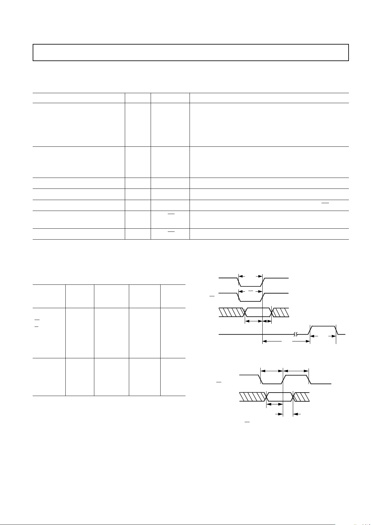
TIMING CHARACTERISTICS
VCC = +15 V, VEE = –15 V, VLL = +5 V, VHI = 2.4 V, VLO = 0.4 V
Limit Limit
Limit –408C to –558C to
Parameter +258C +858C +1258C Units
(Figure la)
t
CS
40 50 55 ns min
t
LI
40 50 55 ns min
t
DS
30 35 40 ns min
t
DH
10 10 15 ns min
t
LH
90 110 120 ns min
t
LW
40 45 45 ns min
(Figure lb)
t
LOW
130 150 165 ns min
t
HIGH
40 45 45 ns min
t
DS
120 140 150 ns min
t
DH
10 10 15 ns min
Specifications subject to change without notice.
Specifications in boldface are tested on all production units at final electrical
test. Results from those tests are used to calculate outgoing quality levels. All
min and max specifications are guaranteed. Those shown in boldface are tested
on all production units.
AC PERFORMANCE CHARACTERISTICS
Parameter Limit Units Test Conditions/Comments
Output Settling Time 13 µs max 20 V Step, TA = +25°C
(Time to ±0.0008% FS 8 µs typ 20 V Step, T
A
= +25°C
with 2 kΩ, 1000 pF Load) 10 µs typ 20 V Step, T
MIN
≤ TA ≤ T
MAX
6 µs typ 10 V Step, TA = +25°C
8 µs typ 10 V Step, T
MIN
≤ TA ≤ T
MAX
2.5 µs typ 1 LSB Step, T
MIN
≤ TA ≤ T
MAX
Total Harmonic Distortion + Noise
A, B, S Grade 0.009 % max 0 dB, 1001 Hz; Sample Rate = 100 kHz; T
A
= +25°C
A, B, S Grade 0.07 % max –20 dB, 1001 Hz; Sample Rate = 100 kHz; T
A
= +25°C
A, B, S Grade 7.0 % max –60 dB, 1001 Hz; Sample Rate = 100 kHz; TA = +25°C
Signal-to-Noise Ratio 83 dB min TA = +25°C
Digital-to-Analog Glitch Impulse 15 nV-s typ DAC Alternately Loaded with 8000H and 7FFFH
Digital Feedthrough 2 nV-s typ DAC Alternately Loaded with 0000H and FFFFH; CS High
Output Noise Voltage 120 nV/√
Hz typ Measured at V
OUT
, 20 V Span; Excludes Reference
Density (1 kHz – 1 MHz)
Reference Noise 125 nV/√Hz typ Measured at REF OUT
Specifications subject to change without notice.
Specifications in boldface are tested on all production units at final electrical test. Results from those tests are used to calculate outgoing quality levels. All min and
max specifications are guaranteed. Those shown in boldface are tested on all production units.
(With the exception of Total Harmonic Distortion + Noise and Signal-to-Noise
Ratio, these characteristics are included for design guidance only and are not subject to test. THD+N and SNR are 100% tested.
T
MIN
≤ TA ≤ T
MAX
, VCC = +15 V, VEE = –15 V, VLL = +5 V except where noted.)
DATA
LDAC
t
DStDH
CS
t
LW
t
LH
L1
t
CS
t
L1
Figure 1a. AD669 Level Triggered Timing Diagram
DATA
t
DS
t
DH
CS AND/OR
L1, LDAC
TIE CS AND/OR
L1 TO GROUND OR TOGETHER WITH LDAC
t
LOW
t
HIGH
Figure 1b. AD669 Edge Triggered Timing Diagram
Page 4
AD669
REV. A
–4–
ORDERING GUIDE
Linearity Gain
Temperature Error Max TC max Package Package
Model Range T
MIN–TMAX
ppm/8C Description Option*
AD669AN –40°C to +85°C ±4 LSB 25 Plastic DIP N-28
AD669AR –40°C to +85°C ±4 LSB 25 SOIC R-28
AD669BN –40°C to +85°C ±2 LSB 15 Plastic DIP N-28
AD669BR –40°C to +85°C ±2 LSB 15 SOIC R-28
AD669AQ –40°C to +85°C ±4 LSB 15 Cerdip Q-28
AD669BQ –40°C to +85°C ±2 LSB 15 Cerdip Q-28
AD669SQ –55°C to +125°C ±4 LSB 15 Cerdip Q-28
AD669/883B** –55°C to +125°C** ** ** **
**N = Plastic DIP; Q = Cerdip; R = SOIC.
**Refer to AD669/883B military data sheet.
ESD SENSITIVITY
The AD669 features input protection circuitry consisting of large transistors and polysilicon series
resistors to dissipate both high-energy discharges (Human Body Model) and fast, low-energy pulses
(Charged Device Model). Per Method 3015.2 of MIL-STD-883: C, the AD669 has been classified
as a Class 2 device.
Proper ESD precautions are strongly recommended to avoid functional damage or performance
degradation. Charges as high as 4000 volts readily accumulate on the human body and test
equipment and discharge without detection. Unused devices must be stored in conductive foam or
shunts, and the foam should be discharged to the destination socket before devices are removed.
For further information on ESD precautions, refer to Analog Devices’ ESD Prevention Manual.
WARNING!
ESD SENSITIVE DEVICE
ABSOLUTE MAXIMUM RATINGS
*
VCC to AGND . . . . . . . . . . . . . . . . . . . . . . . –0.3 V to +17.0 V
V
EE
to AGND . . . . . . . . . . . . . . . . . . . . . . . +0.3 V to –17.0 V
V
LL
to DGND . . . . . . . . . . . . . . . . . . . . . . . . . . –0.3 V to +7 V
AGND to DGND . . . . . . . . . . . . . . . . . . . . . . . . . . . . . . ±1 V
Digital Inputs (Pins 5 through 23) to DGND . . . . . . –1.0 V to
. . . . . . . . . . . . . . . . . . . . . . . . . . . . . . . . . . . . . . . . . . . . +7.0 V
REF IN to AGND . . . . . . . . . . . . . . . . . . . . . . . . . . . . ±10.5 V
Span/Bipolar Offset to AGND . . . . . . . . . . . . . . . . . . . ±10.5 V
REF OUT, V
OUT
. . . . . . Indefinite Short To AGND, DGND,
. . . . . . . . . . . . . . . . . . . . . . . . . . . . . . . . . . . V
CC
, VEE, and V
LL
Power Dissipation (Any Package)
To +60°C . . . . . . . . . . . . . . . . . . . . . . . . . . . . . . . .1000 mW
Derates above +60°C . . . . . . . . . . . . . . . . . . . . . .8.7 mW/°C
Storage Temperature . . . . . . . . . . . . . . . . . . . –65°C to +150°C
Lead Temperature (Soldering, 10 sec) . . . . . . . . . . . . . +300°C
*Stresses above those listed under “Absolute Maximum Ratings” may cause
permanent damage to the device. This is a stress rating only, and functional
operation of the device at these or any other conditions above those indicated in
the operational section of this specification is not implied. Exposure to absolute
maximum rating conditions for extended periods may affect device reliability.
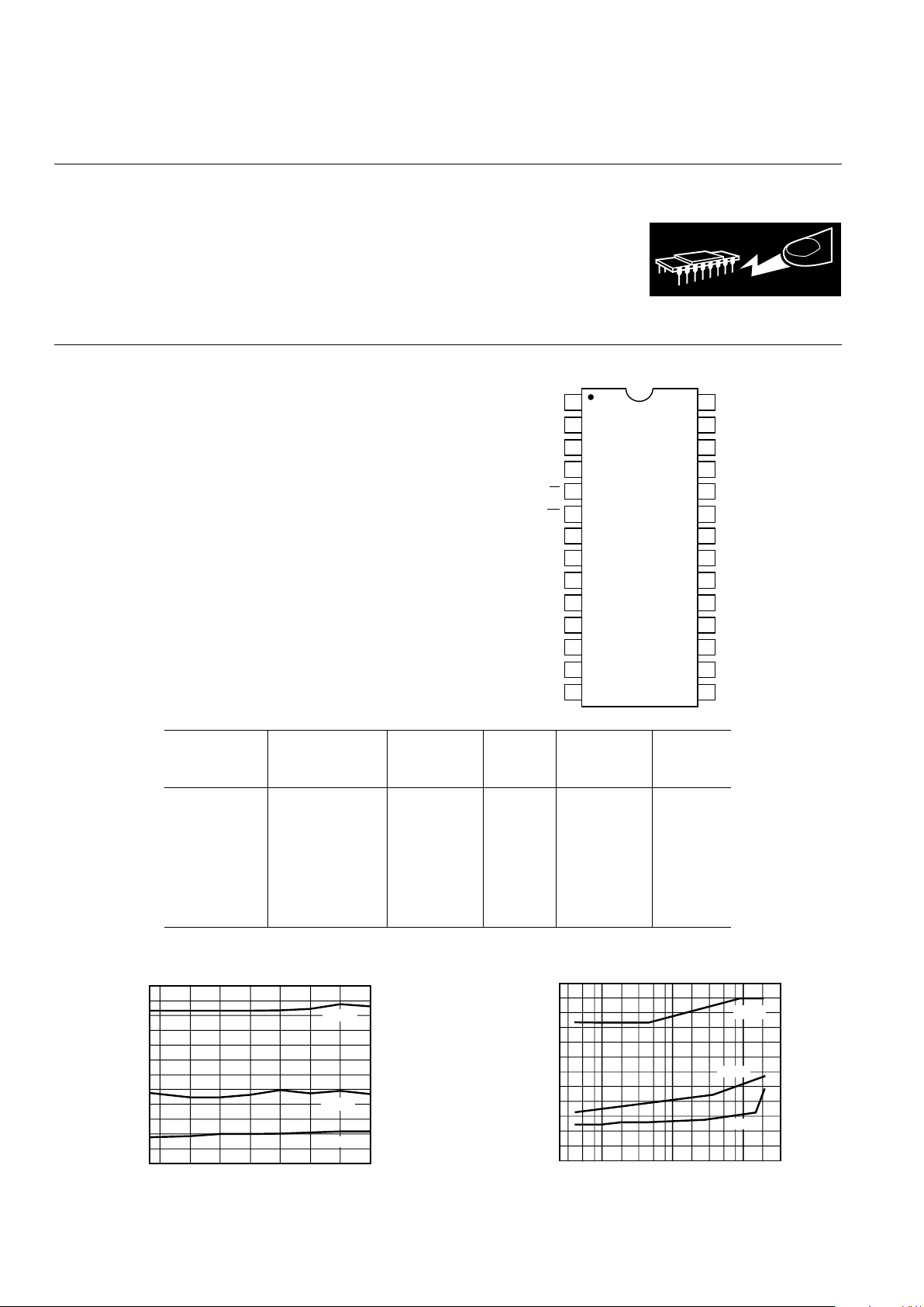
PIN CONFIGURATION
DB15
DB14
DB13
DB12
DB11
DB10
DB9
DB8
DGND
V
EE
V
CC
V
LL
CS
L1
1
2
3
4
5
6
7
8
9
10
11
12
13
14
28
27
26
25
24
23
22
21
20
19
18
17
16
15
TOP VIEW
(Not to Scale)
DB7
DB6
DB5
DB4
DB3
DB2
AGND
LDAC
DB0
DB1
AD669
REF OUT
REF IN
V
OUT
SPAN/BIP
OFFSET
THD + N – %
TEMPERATURE – °C
10
0.001
125
0.01
–25
–50
0.1
1
10075
50250
–60dB
–20dB
0dB
THD+N vs. Temperature
FREQUENCY – Hz
THD + N – %
10
0.001
0.01
0.1
1
100 100001000
–60dB
–20dB
0dB
THD+N vs. Frequency
Page 5

AD669
REV. A
–5–
DEFINITIONS OF SPECIFICATIONS
INTEGRAL NONLINEARITY: Analog Devices defines integral nonlinearity as the maximum deviation of the actual, adjusted DAC output from the ideal analog output (a straight line
drawn from 0 to FS–1 LSB) for any bit combination. This is
also referred to as relative accuracy.
DIFFERENTIAL NONLINEARITY: Differential nonlinearity
is the measure of the change in the analog output, normalized to
full scale, associated with a 1 LSB change in the digital input
code. Monotonic behavior requires that the differential linearity
error be within ±1 LSB over the temperature range of interest.
MONOTONICITY: A DAC is monotonic if the output either
increases or remains constant for increasing digital inputs with
the result that the output will always be a single-valued function
of the input.
GAIN ERROR: Gain error is a measure of the output error between an ideal DAC and the actual device output with all 1s
loaded after offset error has been adjusted out.
OFFSET ERROR: Offset error is a combination of the offset
errors of the voltage-mode DAC and the output amplifier and is
measured with all 0s loaded in the DAC.
BIPOLAR ZERO ERROR: When the AD669 is connected for
bipolar output and 10 . . . 000 is loaded in the DAC, the deviation of the analog output from the ideal midscale value of 0 V is
called the bipolar zero error.
DRIFT: Drift is the change in a parameter (such as gain, offset
and bipolar zero) over a specified temperature range. The drift
temperature coefficient, specified in ppm/°C, is calculated by
measuring the parameter at T
MIN
, 25°C and T
MAX
and dividing
the change in the parameter by the corresponding temperature
change.
TOTAL HARMONIC DISTORTION + NOISE: Total harmonic distortion + noise (THD+N) is defined as the ratio of the
square root of the sum of the squares of the values of the harmonics and noise to the value of the fundamental input frequency. It is usually expressed in percent (%).
THD+N is a measure of the magnitude and distribution of linearity error, differential linearity error, quantization error and
noise. The distribution of these errors may be different, depending upon the amplitude of the output signal. Therefore, to be
the most useful, THD+N should be specified for both large and
small signal amplitudes.
SIGNAL-TO-NOISE RATIO: The signal-to-noise ratio is defined as the ratio of the amplitude of the output when a fullscale signal is present to the output with no signal present. This
is measured in dB.
DIGITAL-TO-ANALOG GLITCH IMPULSE: This is the
amount of charge injected from the digital inputs to the analog
output when the inputs change state. This is measured at half
scale when the DAC switches around the MSB and as many
as possible switches change state, i.e., from 011 . . . 111 to
100 . . . 000.
DIGITAL FEEDTHROUGH: When the DAC is not selected
(i.e.,
CS is held high), high frequency logic activity on the digital inputs is capacitively coupled through the device to show up
as noise on the V
OUT
pin. This noise is digital feedthrough.
THEORY OF OPERATION
The AD669 uses an array of bipolar current sources with MOS
current steering switches to develop a current proportional to
the applied digital word, ranging from 0 mA to 2 mA. A segmented architecture is used, where the most significant four
data bits are thermometer decoded to drive 15 equal current
sources. The lesser bits are scaled using a R-2R ladder, then applied together with the segmented sources to the summing node
of the output amplifier. The internal span/bipolar offset resistor
can be connected to the DAC output to provide a 0 V to +10 V
span, or it can be connected to the reference input to provide a
–10 V to +10 V span.
SPAN/
BIP OFF
AGND
DGND
REF IN
REF OUT
V
OUT
LDAC
DB15
(MSB)
(LSB)
DB0
CS
L1
–V
EE+VCC
+V
LL
16-BIT LATCH
10k
AMP
AD669
22
7
6
5
23
27
28
10V REF
2143
26
24
10k
10.05k
16-BIT LATCH
16-BIT DAC
25
Figure 2. AD669 Functional Block Diagram
ANALOG CIRCUIT CONNECTIONS
Internal scaling resistors provided in the AD669 may be connected to produce a unipolar output range of 0 V to +10 V or a
bipolar output range of –10 V to +10 V. Gain and offset drift
are minimized in the AD669 because of the thermal tracking of
the scaling resistors with other device components.
UNIPOLAR CONFIGURATION
The configuration shown in Figure 3a will provide a unipolar
0 V to +10 V output range. In this mode, 50 Ω resistors are tied
between the span/bipolar offset terminal (Pin 26) and V
OUT
(Pin
25), and between REF OUT (Pin 28) and REF IN (Pin 27). It
is possible to use the AD669 without any external components
by tying Pin 28 directly to Pin 27 and Pin 26 directly to Pin 25.
Eliminating these resistors will increase the gain error by 0.25%
of FSR.
OUTPUT
GND
LDAC
DB15
(MSB)
(LSB)
DB0
CS
L1
–V
EE
+V
CC
+V
LL
16-BIT LATCH
10k
AMP
AD669
22
7
6
5
23
27
28
10V REF
2
1
43
10k
10.05k
16-BIT LATCH
16-BIT DAC
26
25
24
R1
50Ω
R2
50Ω
Figure 3a. 0 V to +10 V Unipolar Voltage Output
Page 6

AD669
REV. A
–6–
If it is desired to adjust the gain and offset errors to zero, this
can be accomplished using the circuit shown in Figure 3b. The
adjustment procedure is as follows:
STEP1 . . . ZERO ADJUST
Turn all bits OFF and adjust zero trimmer, R4, until the output
reads 0.000000 volts (1 LSB = 153 µV).
STEP 2 . . . GAIN ADJUST
Turn all bits ON and adjust gain trimmer, R1, until the output
is 9.999847 volts. (Full scale is adjusted to 1 LSB less than the
nominal full scale of 10.000000 volts).
OUTPUT
GND
LDAC
DB15
(MSB)
(LSB)
DB0
CS
L1
16-BIT LATCH
10k
AMP
AD669
22
7
6
5
23
27
28
10V REF
2
1
4
3
10k
10.05k
16-BIT LATCH
16-BIT DAC
26
25
24
R2
50Ω
R3
16k
R
4
10
+15V
–15V
R1
100Ω
–V
EE
+V
CC
+V
LL
Figure 3b. 0 V to +10 V Unipolar Voltage Output with
Gain and Offset Adjustment
BIPOLAR CONFIGURATION
The circuit shown in Figure 4a will provide a bipolar output
voltage from –10.000000 V to +9.999694 V with positive full
scale occurring with all bits ON. As in the unipolar mode, resistors R1 and R2 may be eliminated altogether to provide AD669
bipolar operation without any external components. Eliminating
these resistors will increase the gain error by 0.50% of FSR in
the bipolar mode.
R1
50Ω
OUTPUT
GND
LDAC
DB15
(MSB)
(LSB)
DB0
CS
L1
16-BIT LATCH
10k
AMP
AD669
227
6
5
23
27
10V REF
2
1
43
26
24
10k
10.05k
16-BIT LATCH
16-BIT DAC
25
28
R2
50Ω
–VEE+V
CC
+V
LL
Figure 4a.±10 V Bipolar Voltage Output
Gain offset and bipolar zero errors can be adjusted to zero using
the circuit shown in Figure 4b as follows:
STEP I . . . OFFSET ADJUST
Turn OFF all bits. Adjust trimmer R2 to give –10.000000 volts
output.
STEP II . . . GAIN ADJUST
Turn all bits ON and adjust R1 to give a reading of +9.999694
volts.
STEP III . . . BIPOLAR ZERO ADJUST
(Optional) In applications where an accurate zero output is required, set the MSB ON, all other bits OFF, and readjust R2
for zero volts output.
100Ω
R1
OUTPUT
GND
LDAC
DB15
(MSB)
(LSB)
DB0
CS
L1
16-BIT LATCH
10k
AMP
AD669
22
7
6
5
23
27
10V REF
2
1
43
26
24
10k
10.05k
16-BIT LATCH
16-BIT DAC
25
28
100Ω
R2
–V
EE
+V
CC
+V
LL
Figure 4b.±10 V Bipolar Voltage Output with Gain and
Offset Adjustment
It should be noted that using external resistors will introduce a
small temperature drift component beyond that inherent in the
AD669. The internal resistors are trimmed to ratio-match and
temperature-track other resistors on chip, even though their absolute tolerances are ±20% and absolute temperature coefficients are approximately –50 ppm/°C . In the case that external
resistors are used, the temperature coefficient mismatch between internal and external resistors, multiplied by the sensitivity of the circuit to variations in the external resistor value, will
be the resultant additional temperature drift.
INTERNAL/EXTERNAL REFERENCE USE
The AD669 has an internal low noise buried Zener diode reference which is trimmed for absolute accuracy and temperature
coefficient. This reference is buffered and optimized for use in a
high speed DAC and will give long-term stability equal or superior to the best discrete Zener diode references. The performance of the AD669 is specified with the internal reference
driving the DAC since all trimming and testing (especially for
gain and bipolar offset) is done in this configuration.
The internal reference has sufficient buffering to drive external
circuitry in addition to the reference currents required for the
DAC (typically 1 mA to REF IN and 1 mA to BIPOLAR OFFSET). A minimum of 2 mA is available for driving external
loads. The AD669 reference output should be buffered with an
external op amp if it is required to supply more than 4 mA total
current. The reference is tested and guaranteed to ±0.2% max
error. The temperature coefficient is comparable to that of the
gain TC for a particular grade.
If an external reference is used (10.000 V, for example), additional trim range should be provided, since the internal reference has a tolerance of ±20 mV, and the AD669 gain and
bipolar offset are both trimmed with the internal reference. The
optional gain and offset trim resistors in Figures 5 and 6 provide
enough adjustment range to null these errors.
It is also possible to use external references other than 10 volts
with slightly degraded linearity specifications. The recommended range of reference voltages is +5 V to +10.24 V, which
Page 7

AD669
REV. A
–7–
allows 5 V, 8.192 V and 10.24 V ranges to be used. For example, by using the AD586 5 V reference, outputs of 0 V to
+5 V unipolar or ±5 V bipolar can be realized. Using the
AD586 voltage reference makes it possible to operate the
AD669 off of ±12 V supplies with 10% tolerances.
Figure 5 shows the AD669 using the AD586 5 V reference in
the bipolar configuration. This circuit includes two optional potentiometers and one optional resistor that can be used to adjust
the gain, offset and bipolar zero errors in a manner similar to
that described in the BIPOLAR CONFIGURATION section.
Use –5.000000 V and +4.999847 as the output values.
50Ω
OUTPUT
GND
LDAC
DB15
(MSB)
(LSB)
DB0
CS
L1
–V
EE+VCC+VLL
AD669
22
7
6
5
23
27
214
3
26
25
R1
100Ω
R2
10kΩ
4
6
5
AD586
+V
CC
28
REF IN
REF OUT
V
OUT
TRIM
GND
SPAN/BIP
OFFSET
24
2
Figure 5. Using the AD669 with the AD586 5 V Reference
USING THE AD669 WITH THE AD688 HIGH PRECISION
VOLTAGE REFERENCE
The AD669 is specified for gain drift from 15 ppm/°C to
25 ppm/°C (depending upon grade) using its internal 10 volt
reference. Since the internal reference contributes the vast majority of this drift, an external high precision voltage reference
will greatly improve performance over temperature. As shown in
Figure 6, the +10 volt output from the AD688 is used as the
AD669 reference. With a 3 ppm/°C drift over the industrial
temperature range, the AD688 will improve the gain drift by a
factor of 5 to a factor of 8 (depending upon the grade of the
AD669 being used). Using this combination may result in apparent increases in initial gain error due to the differences
between the internal reference by which the device is laser
trimmed and the external reference with which the device is actually applied. The AD669 internal reference is specified to be
10 volts ±20 mV whereas the AD688 is specified as 10 volts
±5 mV. This may result in an additional 5 mV (33 LSBs) of apparent initial gain error beyond the specified AD669 gain error.
The circuit shown in Figure 6 also makes use of the –10 V
AD688 output to allow the unipolar offset and gain to be adjusted to zero in the manner described in the UNIPOLAR
CONFIGURATION section.
R2
100Ω
R3
20k
R1
100Ω
LDAC
DB15
(MSB)
(LSB)
DB0
CS
L1
-V
EE
+V
CC
+V
LL
16-BIT LATCH
10k
AMP
AD669
22
7
6
5
23
27
28
10V REF
2
1
43
26
24
10k
10.05k
16-BIT LATCH
16-BIT DAC
25
R4
10kΩ
7
6
3
1
14
15
2
16
5
10 8 12 11
13
R1
R2
R5
R6
R3
AD688
A3
A1
A4
A2
R4
R
S
9
4
GND
OUTPUT
0 TO +10V
+V
CC
–V
EE
Figure 6. Using the AD669 with the AD688 High Precision ±10 V Reference
Page 8

AD669
REV. A
–8–
OUTPUT SETTLING AND GLITCH
The AD669’s output buffer amplifier typically settles to within
0.0008% FS (l/2 LSB) of its final value in 8 µs for a full-scale
step. Figures 7a and 7b show settling for a full-scale and an LSB
step, respectively, with a 2 kΩ, 1000 pF load applied. The guaranteed maximum settling time at +25°C for a full-scale step is
13 µs with this load. The typical settling time for a 1 LSB step is
2.5 µs.
The digital-to-analog glitch impulse is specified as 15 nV-s typi-
cal. Figure 7c shows the typical glitch impulse characteristic at
the code 011 . . . 111 to 100 . . . 000 transition when loading
the second rank register from the first rank register.
20
–10
0
0
+10
10
600
400
200
0
–200
–400
–600
VOLTS
µs
µV
a. –10 V to +10 V Full-Scale Step Settling
50
0
600
400
200
–200
–400
–600
µs
µV
1
234
b. LSB Step Settling
50
0
+10
–10
µs
mV
1
234
c. D-to-A Glitch Impulse
Figure 7. Output Characteristics
DIGITAL CIRCUIT DETAILS
The bus interface logic of the AD669 consists of two independently addressable registers in two ranks. The first rank consists
of a 16-bit register which is loaded directly from a 16-bit microprocessor bus. Once the 16-bit data word has been loaded in the
first rank, it can be loaded into the 16-bit register of the second
rank. This double-buffered organization avoids the generation of
spurious analog output values.
The first rank latch is controlled by
CS and L1. Both of these
inputs are active low and are level-triggered. This means that
data present during the time when both
CS and L1 are low will
enter the latch. When either one of these signals returns high,
the data is latched.
The second rank latch is controlled by LDAC. This input is active high and is also level-triggered. Data that is present when
LDAC is high will enter the latch, and hence the DAC will
change state. When this pin returns low, the data is latched in
the DAC.
Note that LDAC is not gated with
CS or any other control signal. This makes it possible to simultaneously update all of the
AD669’s present in a multi-DAC system by tying the LDAC
pins together. After the first rank register of each DAC has been
individually loaded and latched, the second rank registers are
then brought high together, updating all of the DACs at the
same time. To reduce bit skew, it is suggested to leave 100 ns
between the first rank load and the second rank load.
The first rank latch and second rank latch can be used together
in a master-slave or edge-triggered configuration. This mode of
operation occurs when LDAC and
CS are tied together with L1
tied to ground. Rising edges on the LDAC-
CS pair will update
the DAC with the data presented preceding the edge. The timing diagram for operation in this mode can be seen in Figure lb.
Note, however, that the sum of t
LOW
and t
HIGH
must be long
enough to allow the DAC output to settle to its new value.
Table I. AD669 Truth Table
CS L1 LDAC Operation
0 0 X First Rank Enable
X 1 X First Rank Latched
1 X X First Rank Latched
X X 1 Second Rank Enabled
X X 0 Second Rank Latched
0 0 1 All Latches Transparent
“X” = Don’t Care
It is possible to make the second rank register transparent by tying Pin 23 high. Any data appearing in the first rank register will
then appear at the output of the DAC. It should be noted, however, that the deskewing provided by the second rank latch is
then defeated, and glitch impulse may increase. If it is desired to
make both registers transparent, this can be done by tying Pins
5 and 6 low and Pin 23 high. Table I shows the truth table for
the AD669, while the timing diagram is found in Figure 1.
INPUT CODING
The AD669 uses positive-true binary input coding. Logic “1” is
represented by an input voltage greater than 2.0 V, and Logic
“0” is defined as an input voltage less than 0.8 V.
Page 9

AD669
REV. A
–9–
Unipolar coding is straight binary, where all zeros (0000H) on
the data inputs yields a zero analog output and all ones
(FFFFH) yields an analog output 1 LSB below full scale.
Bipolar coding is offset binary, where an input code of 0000H
yields a minus full-scale output, an input of FFFFH yields an
output 1 LSB below positive full scale, and zero occurs for an
input code with only the MSB on (8000H).
The AD669 can be used with twos complement input coding if
an inverter is used on the MSB (DB15).
DIGITAL INPUT CONSIDERATIONS
The threshold of the digital input circuitry is set at 1.4 volts.
The input lines can thus interface with any type of 5 volt logic.
The AD669 data and control inputs will float to indeterminate
logic states if left open. It is important that
CS and L1 be con-
nected to DGND and Chat LDAC be tied to V
LL
if these pins
are not used.
Fanout for the AD669 is 40 when used with a standard low
power Schottky gate output device.
16-BIT MICROPROCESSOR INTERFACE
The 16-bit parallel registers of the AD669 allow direct interfacing to 16-bit general purpose and DSP microprocessor buses.
The following examples illustrate typical AD669 interface
configurations.
AD669 TO ADSP-2101 INTERFACE
The flexible interface of the AD669 minimizes the required
“glue” logic when it is connected in configurations such as the
one shown in Figure 8. The AD669 is mapped into the ADSP2101’s memory space and requires two wait states using a 12.5
MHz processor clock.
In this configuration, the ADSP-2101 is set up to use the internal timer to interrupt the processor at the desired sample rate.
The
WR pin and data lines D8–D23 from the ADSP-2101 are
tied directly to the
L1 and DB0 through DB15 pins of the
AD669, respectively. The decoded signal
CS1 is connected to
both
CS and LDAC. When a timer interrupt is detected, the
ADSP-2101 automatically vectors to the appropriate service
routine with minimal overhead. The interrupt routine then instructs the processor to execute a data memory write to the address of the AD669.
The
WR pin and CS1 both go low causing the first 16-bit latch
inside the AD669 to be transparent. The data present in the first
rank is then latched by the rising edge of
WR. The rising edge
of
CS1 will cause the second rank 16-bit latch to become
transparent updating the output of the DAC. The length of
WR is extended by two wait states to comply with the timing
requirements of t
LOW
shown in Figure 1b. It is important to
latch the data with the rising edge of
WR rather than the decoded
CS1. This is necessary to comply with the tDH specification of
the AD669.
A0
D8
ADSP-2101
DGND
+5V
DECODER
ADDRESS BUS
LDAC
AD669
DGNDDB0
DATA BUS
DMS
WR
CS1
CS
L1
A13
DB15
D23
V
LL
V
LL
V
OUT
a. ADSP-2101 to AD669 Interface
A13
A12
A11
DMS
CS1
b. Typical Address Decoder
Figure 8. ADSP-2101 to AD669 Interface
Figure 8b shows the circuitry a typical decoder might include.
In this case, a data memory write to any address in the range
3000H to 3400H will result in the AD669 being updated. These
decoders will vary greatly depending on the number of devices
memory-mapped by the processor.
AD669 TO DSP56001 INTERFACE
Figure 9 shows the interface between the AD669 and the
DSP56001. Like the ADSP-2101, the AD669 is mapped into
the DSP56001’s memory space. This application was tested
with a processor clock of 20.48 MHz (t
CYC
= 97.66 ns) although
faster rates are possible.
An external clock connected to the
IRQA pin of the DSP56001
interrupts the processor at the desired sample rate. If ac performance is important, this clock should be synchronous with the
DSP56001 processor clock. Asynchronous clocks will cause jitter on the latch signal due to the uncertainty associated with the
acknowledgment of the interrupt. A synchronous clock is easily
generated by dividing down the clock from the DSP crystal. If
ac performance is not important, it is not necessary for
IRQA to
be synchronous.
After the interrupt is acknowledged, the interrupt routine ini-
tiates a memory write cycle. All of the AD669 control inputs are
Page 10

AD669
REV. A
–10–
tied together which configures the input stage as an edge triggered 16-bit register. The rising edge of the decoded signal
latches the data and updates the output of the DAC. It is necessary to insert wait states after the processor initiates the write
cycle to comply with the timing requirements t
LOW
shown in
Figure 1b. The number of wait states that are required will vary
depending on the processor cycle time. The equation given in
Figure 9 can be used to determine the number of wait states
given the frequency of the processor crystal.
A0–A15
DSP56001
D0–D23
DGND
+5V
EXTERNAL
CLOCK
ADDRESS
DECODE
74F32
LDAC
AD669
DGND
DB0–DB15
XTAL
CS
L1
DS
X/Y
WR
IRQA
V
LL
CS1
T =
1
2 (XTAL)
t – T + 9ns
2T
LOW
# OF
WAIT STATES =
V
LL
Figure 9. DSP56001 to AD669 Interface
As an example, the 20.48 MHz crystal used in this application
results in T = 24.4 ns which means that the required number of
wait states is about 2.76. This must be rounded to the next
highest integer to assure that the minimum pulse widths comply
with those required by the AD669. As the speed of the processor is increased, the data hold time relative to
CS1 decreases. As
processor clocks increase beyond 20.48 MHz, a configuration
such as the one shown for the ADSP-2101 is the better choice.
AD669 TO 8086 INTERFACE
Figure 10 shows the 8086 16-bit microprocessor connected to
multiple AD669s. The double-buffered capability of the AD669
allows the microprocessor to write to each AD669 individually
and then update all the outputs simultaneously. Processor
speeds of 6, 8, and 10 MHz require no wait states to interface
with the AD669.
The 8086 software routine begins by writing a data word to the
CS1 address. The decoder must latch the address using the
ALE signal. The decoded
CS1 pulse goes low causing the first
rank latch of the associated AD669 to become transparent.
Simultaneously, the 8086 places data on the multiplexed bus
which is then latched into the first rank of the AD669 with the
rising edge of the
WR pulse. Care should be taken to prevent
excessive delays through the decoder potentially resulting in a
violation of the AD669 data hold time (t
DH
).
The same procedure is repeated until all three AD669s have had
their first rank latches loaded with the desired data. A final write
command to the LDAC address results in a high-going pulse
that causes the second rank latches of all the AD669s to become
transparent. The falling edge of LDAC latches the data from the
first rank until the next update. This scheme is easily expanded
to include as many AD669s as required.
8086
DGND
+5V
ALE
WR
M/
I0
ADDRESS
DECODE
LDAC
CS1 CS2 CS3
DGND
L1
DB0 – DB15
LDAC
AD669
V
OUT
AD0 – AD15
DGND
L1
DB0 – DB15
LDAC
AD669
V
OUT
DGND
L1
DB0 – DB15
LDAC
AD669
CS
V
OUT
V
LL
V
LL
V
LL
V
LL
CS
CS
Figure 10. 8086-to-AD669 Interface
8-BIT MICROPROCESSOR INTERFACE
The AD669 can easily be operated with an 8-bit bus by the addition of an octal latch. The 16-bit first rank register is loaded
from the 8-bit bus as two bytes. Figure 11 shows the configuration when using a 74HC573 octal latch.
The eight most significant bits are latched into the 74HC573 by
setting the “latch enable” control line low. The eight least significant bits are then placed onto the bus. Now all sixteen bits
can be simultaneously loaded into the first rank register of the
AD669 by setting
CS and L1 low.
8-BIT µP
AND
CONTROL
D7
D0
D7D0Q7
Q0
74HC573
11
LDAC
MSB
DB8
DB7
LSB
AD669
CS1 L1
Figure 11. Connections for 8-Bit Bus Interface
Page 11

AD669
REV. A
–11–
NOISE
In high resolution systems, noise is often the limiting factor. A
16-bit DAC with a 10 volt span has an LSB size of 153 µV
(–96 dB). Therefore, the noise floor must remain below this
level in the frequency range of interest. The AD669’s noise
spectral density is shown in Figures 12 and 13. Figure 12 shows
the DAC output noise voltage spectral density for a 20 V span
excluding the reference. This figure shows the l/f corner frequency
at 100 Hz and the wideband noise to be below 120 nV/√
Hz.
Figure 13 shows the reference noise voltage spectral density.
This figure shows the reference wideband noise to be below
125 nV/√
Hz.
1000
1
11M
100
10
10 100k10k1k100 10M
FREQUENCY – Hz
NOISE VOLTAGE – nV/ Hz
Figure 12. DAC Output Noise Voltage Spectral Density
1000
1
1
1M
100
10
10 100k
10k1k100
10M
FREQUENCY – Hz
NOISE VOLTAGE – nV/ Hz
Figure 13. Reference Noise Voltage Spectral Density
BOARD LAYOUT
Designing with high resolution data converters requires careful
attention to board layout. Trace impedance is the first issue. A
306 µA current through a 0.5 Ω trace will develop a voltage
drop of 153 µV, which is 1 LSB at the 16-bit level for a 10 V
full-scale span. In addition to ground drops, inductive and capacitive coupling need to be considered, especially when high
accuracy analog signals share the same board with digital signals. Finally, power supplies need to be decoupled in order to
filter out ac noise.
Analog and digital signals should not share a common path.
Each signal should have an appropriate analog or digital return
routed close to it. Using this approach, signal loops enclose a
small area, minimizing the inductive coupling of noise. Wide PC
tracks, large gauge wire, and ground planes are highly recommended to provide low impedance signal paths. Separate analog
and digital ground planes should also be utilized, with a single
interconnection point to minimize ground loops. Analog signals
should be routed as far as possible from digital signals and
should cross them at right angles.
One feature that the AD669 incorporates to help the user layout
is the analog pins (V
CC
, VEE, REF OUT, REF IN, SPAN/BIP
OFFSET, V
OUT
and AGND) are adjacent to help isolate analog
signals from digital signals.
SUPPLY DECOUPLING
The AD669 power supplies should be well filtered, well regulated, and free from high frequency noise. Switching power supplies are not recommended due to their tendency to generate
spikes which can induce noise in the analog system.
Decoupling capacitors should be used in very close layout proximity between all power supply pins and ground. A 10 µF tanta-
lum capacitor in parallel with a 0.1 µF ceramic capacitor
provides adequate decoupling. V
CC
and VEE should be bypassed
to analog ground, while V
LL
should be decoupled to digital
ground.
An effort should be made to minimize the trace length between
the capacitor leads and the respective converter power supply
and common pins. The circuit layout should attempt to locate
the AD669, associated analog circuitry and interconnections as
far as possible from logic circuitry. A solid analog ground plane
around the AD669 will isolate large switching ground currents.
For these reasons, the use of wire wrap circuit construction
is not recommended; careful printed circuit construction is
preferred.
GROUNDING
The AD669 has two pins, designated analog ground (AGND)
and digital ground (DGND.) The analog ground pin is the
“high quality” ground reference point for the device. Any external loads on the output of the AD669 should be returned to
analog ground. If an external reference is used, this should also
be returned to the analog ground.
If a single AD669 is used with separate analog and digital
ground planes, connect the analog ground plane to AGND and
the digital ground plane to DGND keeping lead lengths as short
as possible. Then connect AGND and DGND together at the
AD669. If multiple AD669s are used or the AD669 shares analog supplies with other components, connect the analog and
digital returns together once at the power supplies rather than at
each chip. This single interconnection of grounds prevents large
ground loops and consequently prevents digital currents from
flowing through the analog ground.
Page 12

AD669
REV. A
–12–
C1555–10–11/91
PRINTED IN U.S.A.
 Loading...