

Page 1
Quad IF Receiver
AD6657A
Rev. 0
Trademarks and registered trademarks are the prop erty of their respective owner s.
Fax: 781.461.3113 ©2011 Analog Devices, Inc. All rights reserved.
VIN+A
DO±AB
D10±AB
VIN–A
PIPELINE
ADC
NOISE SHAPING
REQUANTIZER
VIN+B
VIN–B
PIPELINE
ADC
VIN+C
VIN–C
PIPELINE
ADC
VIN+D
VIN–D
PIPELINE
ADC
SERIAL PO RT
REFERENCE
14
11
NOISE SHAPING
REQUANTIZER
PORT A
AD6657A
PORT B
DATA MULTIPLEXER
AND LVDS DRIVERS
14
11
NOISE SHAPING
REQUANTIZER
14
11
NOISE SHAPING
REQUANTIZER
CLOCK
DIVIDER
09684-001
14
11
VCMA
VCMB
VCMC
VCMD
SCLK SDIO CSB CLK+
AVDD
AGND
DRVDD
DRGND
CLK–
DO±CD
DCO±AB
DCO±CD
D10±CD
MODE
SYNC
PDWN
Data Sheet
FEATURES
11-bit, 200 MSPS output data rate per channel
Integrated noise shaping requantizer
Performance with NSR enabled
SNR: 76.0 dBFS in 40 MHz band to 70 MHz at 185 MSPS
SNR: 73.6 dBFS in 60 MHz band to 70 MHz at 185 MSPS
SNR: 72.8 dBFS in 65 MHz band to 70 MHz at 185 MSPS
Performance with NSR disabled
SNR: 66.5 dBFS to 70 MHz at 185 MSPS
SFDR: 88 dBc to 70 MHz at 185 MSPS
Low power: 1.2 W at 185 MSPS
1.8 V analog supply operation
1.8 V LVDS (ANSI-644 levels) output
1-to-8 integer clock divider
Internal ADC voltage reference
1.75 V p-p analog input range (programmable to 2.0 V p-p)
Differential analog inputs with 800 MHz bandwidth
95 dB channel isolation/crosstalk
Serial port control
User-configurable built-in self test (BIST) capability
Energy saving power-down modes
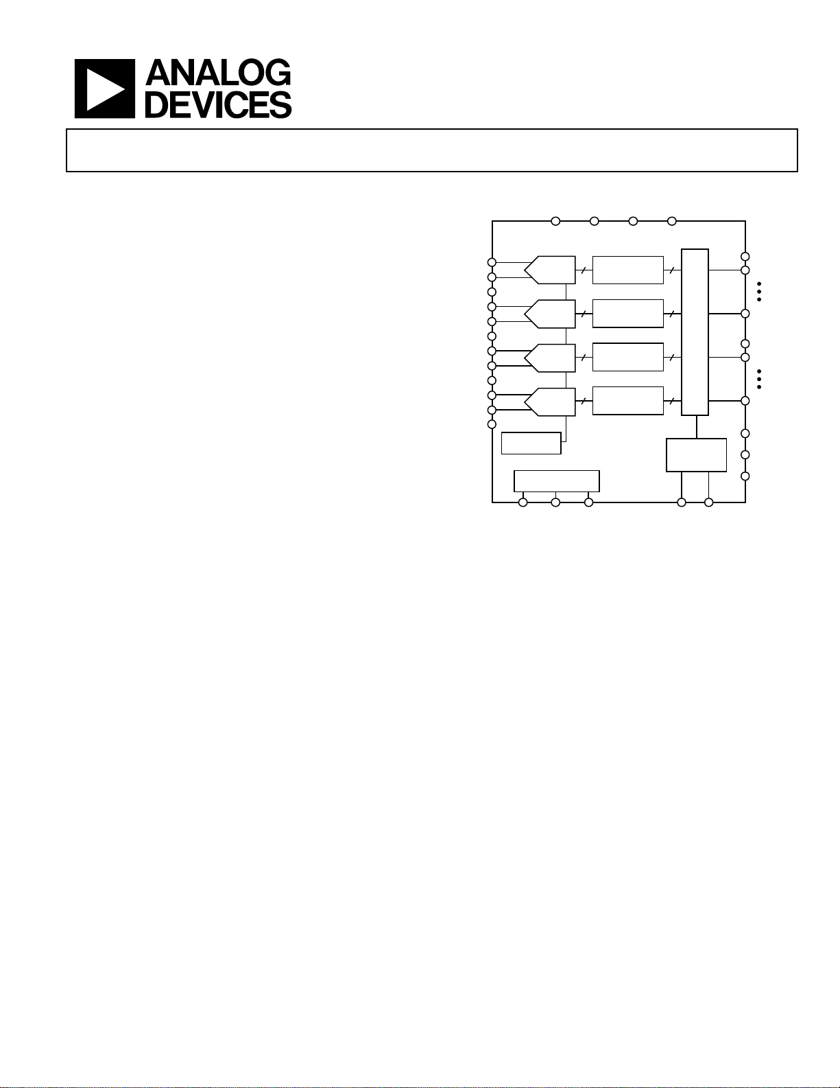
FUNCTIONAL BLOCK DIAGRAM
Figure 1.
APPLICATIONS
Communications
Diversity radio and smart antenna (MIMO) systems
Multimode digital receivers (3G)
WCDMA, LTE, CDMA2000
WiMAX, TD-SCDMA
I/Q demodulation systems
General-purpose software radios
GENERAL DESCRIPTION
The AD6657A is an 11-bit, 200 MSPS, quad channel intermediate
frequency (IF) receiver specifically designed to support multiple
antenna systems in telecommunication applications where high
dynamic range performance, low power, and small size are desired.
The device consists of four high performance ADCs and NSR
digital blocks. Each ADC consists of a multistage, differential
pipelined architecture with integrated output error correction
logic. The ADC features a wide bandwidth switched capacitor
sampling network within the first stage of the differential pipeline.
An integrated voltage reference eases design considerations. A
duty cycle stabilizer (DCS) compensates for variations in the
ADC clock duty cycle, allowing the converters to maintain
excellent performance.
Information furnished by Analog Devices is believed to be accurate and reliable. However, no
responsibility is assumed by Analog Devices for its use, nor for any infringements of patents or other
rights of third parties that may result from its use. Specifications subject to change without notice. No
license is granted by implication or otherwise under any patent or patent rights of Analog Devices.
Each ADC output is connected internally to an NSR block. The
integrated NSR circuitry allows for improved SNR performance
in a smaller frequency band within the Nyquist bandwidth. The
device supports two different output modes selectable via the
external MODE pin or the serial port interface (SPI).
With the NSR feature enabled, the outputs of the ADCs are
processed such that the AD6657A supports enhanced SNR performance within a limited portion of the Nyquist bandwidth
while maintaining an 11-bit output resolution. The NSR block
can be programmed to provide a bandwidth of either 22%, 33%,
or 36% of the sample clock. For example, with a sample clock
rate of 185 MSPS, the AD6657A can achieve up to 76.0 dBFS
SNR for a 40 MHz bandwidth in the 22% mode, up to 73.6 dBFS
SNR for a 60 MHz bandwidth in the 33% mode, or up to 72.8 dBFS
SNR for a 65 MHz bandwidth in the 36% mode.
(General Description continued on Page 3)
One Technology Way, P.O. Box 9106, Norwood, MA 02062-9106, U.S.A.
Tel: 781.329.4700 www.analog.com
Page 2

AD6657A Data Sheet
TABLE OF CONTENTS
Features .............................................................................................. 1
Applications ....................................................................................... 1
Functional Block Diagram .............................................................. 1
General Description ......................................................................... 1
Revision History ............................................................................... 2
Product Highlights ........................................................................... 3
Specifications ..................................................................................... 4
DC Specifications ......................................................................... 4
AC Specifications .......................................................................... 5
Digital Specifications ................................................................... 7
Switching Specifications .............................................................. 9
Timing Specifications ................................................................ 10
Absolute Maximum Ratings ..................................................... 11
Thermal Characteristics ............................................................ 11
ESD Caution ................................................................................ 11
Pin Configuration and Function Descriptions ........................... 12
Typical Performance Characteristics ........................................... 14
Equivalent Circuits ......................................................................... 18
Theory of Operation ...................................................................... 19
ADC Architecture ...................................................................... 19
Analog Input Considerations .................................................... 19
Clock Input Considerations ...................................................... 21
Power Dissipation and Standby Mode ..................................... 23
Channel/Chip Synchronization ................................................ 23
Digital Outputs ........................................................................... 24
Timing ......................................................................................... 24
Noise Shaping Requantizer ........................................................... 25
22% BW Mode (>40 MHz at 184.32 MSPS) ........................... 25
33% BW Mode (>60 MHz at 184.32 MSPS) ........................... 26
36% BW Mode (>65 MHz at 184.32 MSPS) ........................... 27
MODE Pin ................................................................................... 27
Built-In Self Test (BIST) and Output Test ................................... 28
BIST .............................................................................................. 28
Output Test Modes ..................................................................... 28
Serial Port Interface (SPI) .............................................................. 29
Configuration Using the SPI ..................................................... 29
Hardware Interface ..................................................................... 29
Memory Map .................................................................................. 30
Reading the Memory Map Register Table ............................... 30
Memory Map Register Table ..................................................... 31
Memory Map Register Descriptions ........................................ 33
Applications Information .............................................................. 35
Design Guidelines ...................................................................... 35
Packaging and Ordering Information ......................................... 36
Outline Dimensions ................................................................... 36
Ordering Guide .......................................................................... 36
REVISION HISTORY
10/11—Revision 0: Initial Version
Rev. 0 | Page 2 of 36
Page 3

Data Sheet AD6657A
With the NSR block disabled, the ADC data is provided directly to
the output with a resolution of 11 bits. The AD6657A can achieve
up to 66.5 dBFS SNR for the entire Nyquist bandwidth when
operated in this mode. This allows the AD6657A to be used in
telecommunication applications such as a digital predistortion
observation path where wider bandwidths are used.
After digital signal processing, multiplexed output data is
routed into two 11-bit output ports such that the maximum
digital data rate (DDR) is 400 Mbps. These outputs are set at
1.8 V LVDS and support ANSI-644 levels.
The AD6657A receiver digitizes a wide spectrum of IF frequencies.
Each receiver is designed for simultaneous reception of a separate
antenna. This IF sampling architecture greatly reduces component
cost and complexity compared with traditional analog techniques
or less integrated digital methods.
Flexible power-down options allow significant power savings.
Programming for device setup and control is accomplished
using a 3-wire SPI-compatible serial interface with numerous
modes to support board level system testing.
The AD6657A is available in a Pb-free, RoHS compliant,
144-ball, 10 mm × 10 mm chip scale package ball grid array
(CSP_BGA) that is specified over the industrial temperature
range of −40°C to +85°C.
PRODUCT HIGHLIGHTS
1. Four analog-to-digital converters (ADCs) are contained in
a small, space-saving, 10 mm × 10 mm × 1.4 mm, 144-ball
CSP_BGA package.
2. Pin selectable noise shaping requantizer (NSR) function
that allows for improved SNR within a reduced bandwidth
of up to 65 MHz at 185 MSPS.
3. LVDS digital output interface configured for low cost
FPGA families.
4. 230 mW per ADC core power consumption.
5. Operation from a single 1.8 V supply.
6. Standard SPI that supports various product features and
functions, such as data formatting (offset binary or twos
complement), NSR, power-down, test modes, and voltage
reference mode.
7. On-chip integer 1-to-8 input clock divider and multichip
sync function to support a wide range of clocking schemes
and multichannel subsystems.
Rev. 0 | Page 3 of 36
Page 4

AD6657A Data Sheet
Differential Nonlinearity (DNL)1
Full
−0.4
±0.1
+0.4
LSB
Offset Error
Full
−5
+3
+11
mV
TEMPERATURE DRIFT
ANALOG INPUT
SPECIFICATIONS
DC SPECIFICATIONS
AVDD = 1.8 V, DRVDD = 1.8 V, fS = 185 MSPS, 1.75 V p-p differential input, VIN = −1.0 dBFS differential input, and default SPI, unless
otherwise noted.
Table 1.
Parameter Temperature Min Typ Max Unit
RESOLUTION Full 11 Bits
ACCURACY
No Missing Codes Full Guaranteed
Offset Error Full −0.9 +0.1 +0.9 mV
Gain Error Full +4 +11 +18 % FSR
Integral Nonlinearity (INL)
1
Full −
0.55 ±0.17 +0.55 LSB
MATCHING CHARACTERISTIC
Gain Error Full 0 +2.1 +8 % FSR
Offset Error Full 2 ppm/°C
Gain Error Full 40 ppm/°C
Input Range Full 1.4 1.75 2.0 V p-p
Input Common-Mode Voltage Full 0.95 V
Input Resistance (Differential) Full 20 kΩ
Input Capacitance2 Full 5 pF
POWER SUPPLIES
Supply Voltage
AVDD Full 1.7 1.8 1.9 V
DRVDD Full 1.7 1.8 1.9 V
Supply Current
1
Full 466 510 mA
I
AVDD
1
(1.8 V LVDS) Full 170 183 mA
I
DRVDD
POWER CONSUMPTION
Sine Wave Input1 Full 1145 1247 mW
Standby Power3 Full 129 mW
Power-Down Power Full 3.8 10 mW
1
Measured with a 10 MHz, 0 dBFS sine wave, with 100 Ω termination on each LVDS output pair.
2
Input capacitance refers to the effective capacitance between one differential input pin and AGND.
3
Standby power is measured with a dc input and the CLKx pins inactive (set to AVDD or AGND).
Rev. 0 | Page 4 of 36
Page 5

Data Sheet AD6657A
fIN = 170 MHz
25°C 66.3 dBFS
SIGNAL-TO-NOISE-RATIO (SNR)—NSR ENABLED
fIN = 70 MHz
25°C 73.3 dBFS
fIN = 50 MHz
25°C 72.6 dBFS
fIN = 70 MHz
25°C 65.5 dBFS
AC SPECIFICATIONS
AVDD = 1.8 V, DRVDD = 1.8 V, fS = 185 MSPS, 1.75 V p-p differential input, VIN = −1.0 dBFS differential input, and default SPI, unless
otherwise noted.
Table 2.
Parameter1 Temperature Min Typ Max Unit
SIGNAL-TO-NOISE-RATIO (SNR)—NSR DISABLED
fIN = 10 MHz 25°C 66.6 dBFS
fIN = 50 MHz 25°C 66.5 dBFS
fIN = 70 MHz 25°C 66.5 dBFS
Full 65.6 dBFS
fIN = 250 MHz 25°C 65.9 dBFS
22% BW Mode
fIN = 10 MHz 25°C 76.0 dBFS
fIN = 50 MHz 25°C 75.7 dBFS
fIN = 70 MHz 25°C 75.7 dBFS
fIN = 170 MHz 25°C 74.3 dBFS
Full 72.9 dBFS
fIN = 250 MHz 25°C 72.8 dBFS
33% BW Mode
fIN = 10 MHz 25°C 73.6 dBFS
fIN = 50 MHz 25°C 73.6 dBFS
fIN = 170 MHz 25°C 72.5 dBFS
Full 71.3 dBFS
fIN = 230 MHz 25°C 71.2 dBFS
36% BW Mode
fIN = 10 MHz 25°C 72.8 dBFS
fIN = 70 MHz 25°C 72.6 dBFS
fIN = 170 MHz 25°C 71.8 dBFS
Full 70.7 dBFS
fIN = 250 MHz 25°C 70.8 dBFS
SIGNAL-TO-NOISE-AND DISTORTION (SINAD)
fIN = 10 MHz 25°C 65.5 dBFS
fIN = 50 MHz 25°C 65.5 dBFS
fIN = 170 MHz 25°C 65.3 dBFS
Full 64.6 dBFS
fIN = 250 MHz 25°C 64.8 dBFS
EFFECTIVE NUMBER OF BITS (ENOB)
fIN = 10 MHz 25°C 10.6 Bits
fIN = 50 MHz 25°C 10.6 Bits
fIN = 70 MHz 25°C 10.6 Bits
fIN = 170 MHz 25°C 10.6 Bits
fIN = 250 MHz 25°C 10.5 Bits
Rev. 0 | Page 5 of 36
Page 6

AD6657A Data Sheet
fIN = 170 MHz
25°C −90 dBc
SPURIOUS-FREE DYNAMIC RANGE (SFDR)
fIN = 250 MHz
25°C 83 dBc
ANALOG INPUT BANDWIDTH
25°C 800 MHz
Parameter1 Temperature Min Typ Max Unit
WORST SECOND OR THIRD HARMONIC
fIN = 10 MHz 25°C −94 dBc
fIN = 50 MHz 25°C −91 dBc
fIN = 70 MHz 25°C −88 dBc
Full −80 dBc
fIN = 250 MHz 25°C −83 dBc
fIN = 10 MHz 25°C 94 dBc
fIN = 50 MHz 25°C 91 dBc
fIN = 70 MHz 25°C 88 dBc
fIN = 170 MHz 25°C 90 dBc
Full 80 dBc
WORST OTHER HARMONIC (FOURTH THROUGH EIGHTH)
fIN = 10 MHz 25°C −94 dBc
fIN = 50 MHz 25°C −95 dBc
fIN = 70 MHz 25°C −94 dBc
fIN = 170 MHz 25°C −94 dBc
Full −80 dBc
fIN = 250 MHz 25°C −90 dBc
TWO TONE SFDR (−7 dBFS)
f
= 169 MHz, f
IN1
CROSSTALK2 Full 95 dB
= 172 MHz 25°C 89 dBc
IN2
1
See the AN-835 Application Note, Understanding High Speed ADC Testing and Evaluation, for a complete set of definitions.
2
Crosstalk is measured at 155 MHz with −1 dBFS on one channel and no input on the alternate channel.
Rev. 0 | Page 6 of 36
Page 7

Data Sheet AD6657A
Input Voltage Range
Full
AGND − 0.3
AVDD + 0.2
V
Input Capacitance
Full 4 pF
Low Level Input Current
Full
−100
+100
µA
LOGIC INPUT (CSB)1
High Level Input Current
Full
−10 +10
µA
DIGITAL SPECIFICATIONS
AVDD = 1.8 V, DRVDD = 1.8 V, fS = 185 MSPS, 1.75 V p-p differential input, VIN = −1.0 dBFS differential input, and default SPI, unless
otherwise noted.
Table 3.
Parameter Temperature Min Typ Max Unit
DIFFERENTIAL CLOCK INPUTS (CLK+, CLK−)
Logic Compliance CMOS/LVDS/LVPECL
Internal Common-Mode Bias Full 0.9 V
Differential Input Voltage Full 0.2 3.6 V p-p
High Level Input Voltage Full 1.2 2.0 V
Low Level Input Voltage Full 0 0.8 V
High Level Input Current Full −10 +10 µA
Low Level Input Current Full −10 +10 µA
Input Resistance Full 8 10 12 kΩ
SYNC INPUT
Logic Compliance CMOS
Internal Bias Full 0.9 V
Input Voltage Range Full AGND AVDD V
High Level Input Voltage Full 1.2 AVDD V
Low Level Input Voltage Full AGND 0.6 V
High Level Input Current Full −100 +100 µA
Input Resistance Full 12 16 20 kΩ
Input Capacitance Full 1 pF
High Level Input Voltage Full 1.22 2.1 V
Low Level Input Voltage Full 0 0.6 V
High Level Input Current Full −10 +10 µA
Low Level Input Current Full 40 132 µA
Input Resistance Full 26 kΩ
Input Capacitance Full 2 pF
LOGIC INPUT (SCLK)2
High Level Input Voltage Full 1.22 2.1 V
Low Level Input Voltage Full 0 0.6 V
High Level Input Current Full −92 −135 µA
Low Level Input Current Full −10 +10 µA
Input Resistance Full 26 kΩ
Input Capacitance Full 2 pF
LOGIC INPUT/OUTPUT (SDIO)
High Level Input Voltage Full 1.22 2.1 V
Low Level Input Voltage Full 0 0.6 V
Low Level Input Current Full 38 128 µA
Input Resistance Full 26 kΩ
Input Capacitance Full 5 pF
2
Rev. 0 | Page 7 of 36
Page 8

AD6657A Data Sheet
Parameter Temperature Min Typ Max Unit
LOGIC INPUT (MODE)1
High Level Input Voltage Full 1.22 2.1 V
Low Level Input Voltage Full 0 0.6 V
High Level Input Current Full −10 +10 μA
Low Level Input Current Full 40 132 μA
Input Resistance Full 26 kΩ
Input Capacitance Full 2 pF
LOGIC INPUT (PDWN)2
High Level Input Voltage Full 1.22 2.1 V
Low Level Input Voltage Full 0 0.6 V
High Level Input Current Full −90 −134 μA
Low Level Input Current Full −10 +10 μA
Input Resistance Full 26 kΩ
Input Capacitance Full 5 pF
DIGITAL OUTPUTS (LVDS)
Differential Output Voltage (VOD) Full 247 454 mV
Output Offset Voltage (VOS) Full 1.125 1.375 V
1
Pull up.
2
Pull down.
Rev. 0 | Page 8 of 36
Page 9
Data Sheet AD6657A
Aperture Delay (tA)2
Full 1.3 ns
Data Propagation Delay (tPD)2
Full
3.0
4.0
4.9
ns
N – 1
N + 1
N + 2
N + 3
N + 4
N + 5
N
CLK+
CLK–
DCO+
DCO–
D10+AB (MSB)
D10–AB (MSB)
D0+AB (LSB)
D0–AB (LSB)
VIN
t
A
t
CH
t
DCO
t
CL
t
PD
t
SKEW
1/
f
S
D10A D10B D10A D10B D10A D10B D10A D10B D10A D10B D10A D10B
D0A D0B
D10A D10B
D0A D0B D0A D0B D0A D0B D0A D0B D0A D0B D0A D0B
09684-002
SWITCHING SPECIFICATIONS
AVDD = 1.8 V, DRVDD = 1.8 V, fS = 185 MSPS, 1.75 V p-p differential input, VIN = −1.0 dBFS differential input, and default SPI, unless
otherwise noted.
Table 4.
Parameter Temperature Min Typ Max Unit
CLOCK INPUT PARAMETERS
Input Clock Rate Full 625 MHz
Conversion Rate1 Full 40 185 200 MSPS
CLK Pulse Width High (tCH)2 Full 2.7 ns
Aperture Uncertainty (Jitter, tJ) Full 0.13 ps rms
DATA OUTPUT PARAMETERS
DCO Propagation Delay (t
DCO to Data Skew (t
SKEW
)2 Full 3.1
DCO
)2 Full −41 +6.1 +33 ns
4.0
4.9 ns
Pipeline Delay (Latency) Full 9 Cycles
With NSR Enabled Full 12 Cycles
Wake-Up Time (from Standby)3 Full 0.5 µs
Wake-Up Time (from Power Down)3 Full 310 µs
OUT-OF-RANGE RECOVERY TIME Full 2 Cycles
1
Conversion rate is the clock rate after the divider.
2
See Figure 2 for details.
3
Wake-up time is dependent on the value of the decoupling capacitors.
Data Output Timing Diagram
Figure 2. Data Output Timing (Timing for Channel C and Channel D Is Identical to Timing for Channel A and Channel B)
Rev. 0 | Page 9 of 36
Page 10
AD6657A Data Sheet
tDH
Hold time between the data and the rising edge of SCLK
2
ns
t
10
ns
SYNC
CLK+
t
HSYNC
t
SSYNC
09684-003
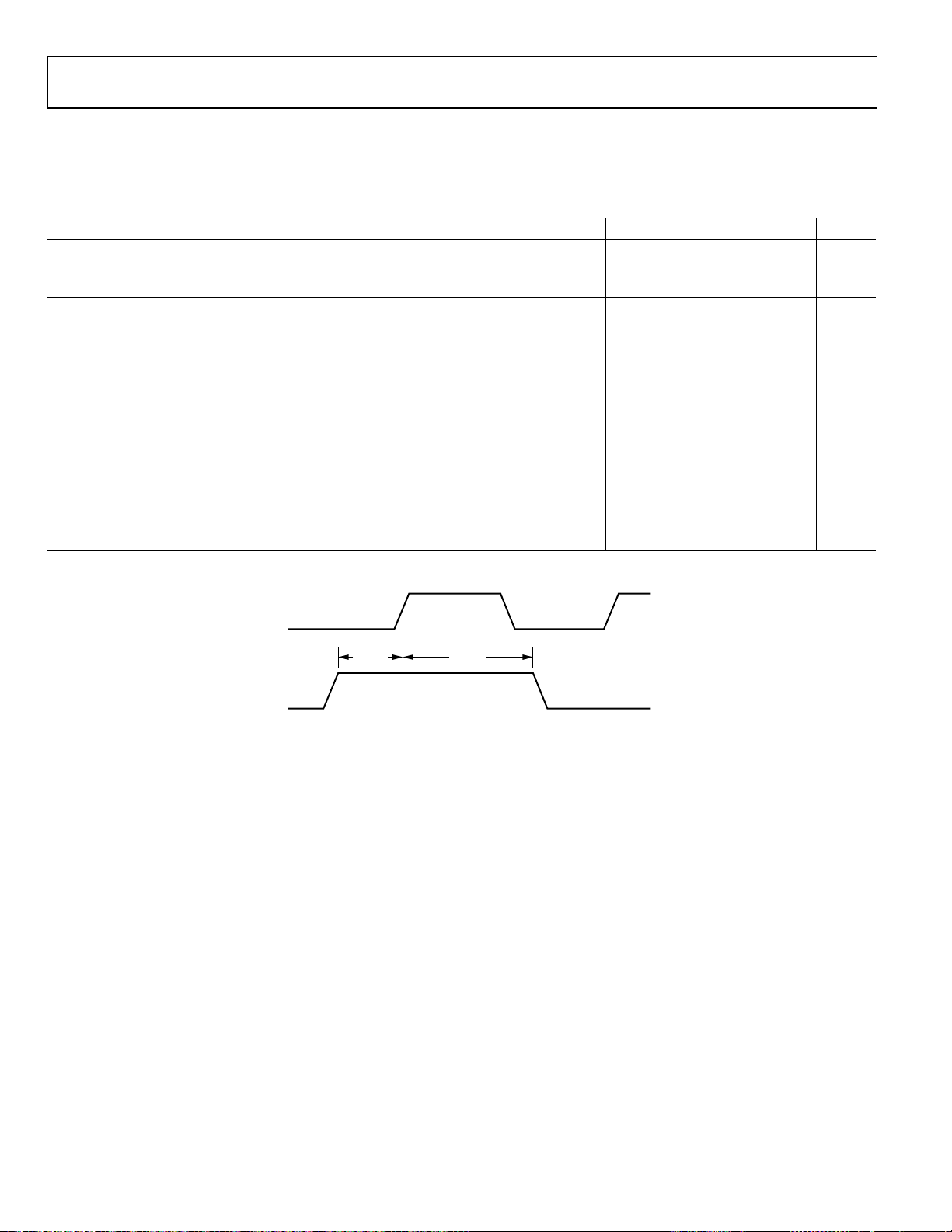
TIMING SPECIFICATIONS
AVDD = 1.8 V, DRVDD = 1.8 V, fS = 185 MSPS, 1.75 V p-p differential input, VIN = −1.0 dBFS differential input, and default SPI, unless
otherwise noted.
Table 5.
Parameter Description Min Typ Max Unit
SYNC TIMING REQUIREMENTS See Figure 3 for details
t
SYNC to rising edge of CLK setup time 0.24 ns
SSYNC
t
SYNC to rising edge of CLK hold time 0.40 ns
HSYNC
SPI TIMING REQUIREMENTS See Figure 60 for details, except where noted
tDS Setup time between the data and the rising edge of SCLK 2 ns
t
Period of the SCLK 40 ns
CLK
tS Setup time between CSB and SCLK 2 ns
tH Hold time between CSB and SCLK 2 ns
t
SCLK pulse width high 10 ns
HIGH
t
SCLK pulse width low 10 ns
LOW
EN_SDIO
t
DIS_SDIO
Time required for the SDIO pin to switch from an input to
an output relative to the SCLK falling edge (not pictured in
Figure 60)
Time required for the SDIO pin to switch from an output to
an input relative to the SCLK rising edge (not pictured in
Figure 60)
10 ns
Sync Input Timing Diagram
Figure 3. SYNC Input Timing Requirements
Rev. 0 | Page 10 of 36
Page 11
Data Sheet AD6657A
v
ABSOLUTE MAXIMUM RATINGS
Table 6.
Parameter Rating
AVDD to AGND −0.3 V to +2.0 V
DRVDD to AGND −0.3 V to +2.0 V
VIN+x, VIN−x to AGND −0.3 V to AVDD + 0.2 V
CLK+, CLK− to AGND −0.3 V to AVDD + 0.2 V
SYNC to AGND −0.3 V to AVDD + 0.2 V
VCMx to AGND −0.3 V to AVDD + 0.2 V
CSB to AGND −0.3 V to DRVDD + 0.2 V
SCLK to AGND −0.3 V to DRVDD + 0.2 V
SDIO to AGND −0.3 V to DRVDD + 0.2 V
PDWN to AGND −0.3 V to DRVDD + 0.2 V
MODE to AGND −0.3 V to DRVDD + 0.2 V
Digital Outputs to AGND −0.3 V to DRVDD + 0.2 V
DCO+AB, DCO−AB, DCO+CD,
−0.3 V to DRVDD + 0.2 V
DCO−CD to AGND
Operating Temperature Range
−40°C to +85°C
(Ambient)
Maximum Junction Temperature
150°C
Under Bias
Storage Temperature Range
−65°C to +150°C
(Ambient)
Stresses abovethose listedunderAbsoluteMaximumRatings
may cause permanent damage to the device. This is a stress
rating only; functional operation of the device at these or any
other conditions above those indicated in the operational
section of this specification is not implied. Exposure to absolute
maximumratingconditionsfor extendedperiodsmayaffect
de
ice reliability.
THERMAL CHARACTERISTICS
The values in Table 7 are per JEDEC JESD51-7 and JEDEC
JESD25-5 for a 2S2P test board. Typical θ
4-layer printed circuit board (PCB) with a solid ground plane.
As shown in Table 7, airflow improves heat dissipation, which
reduces θ
. In addition, metal in direct contact with the
JA
package leads from metal traces, through holes, ground, and
power planes reduces θ
.
JA
Table 7.
Airflow
Package Type
Velocity θ
144-Ball CSP_BGA 0 m/s 26.9 8.9 6.6 °C/W
1 m/s 24.2 °C/W
2.5 m/s 23.0 °C/W
1
Per JEDEC JESD51-2 (still air) or JEDEC JESD51-6 (moving air).
2
Per MIL-STD 883, Method 1012.1.
3
Per JEDEC JESD51-8 (still air).
The values in Table 8 are from simulations. The PCB is a JEDEC
multilayer board. Thermal performance for actual applications
requires careful inspection of the conditions in the application
to determine whether they are similar to those assumed in these
calculations.
Table 8.
Airflow
Package Type
Veloc ity
144-Ball CSP_BGA 0 m/s 14.4 0.23 °C/W
1 m/s 14.0 0.50 °C/W
2.5 m/s 13.9 0.53 °C/W
is specified for a
JA
1
JA
2
θ
JC
JB
3
θ
JB
JT
Unit
Unit
ESD CAUTION
Rev. 0 | Page 11 of 36
Page 12

AD6657A Data Sheet
G1 to G12
DRGND
Ground
Digital Output Driver Ground.
M7
D1+AB
Output
Channel A and Channel B LVDS Output Data 1—True.
AGND VIN+C VIN–C AGND AVDD CLK– CLK+ AVDD AGND VIN–B VIN+B AG
ND
1 2 3 4 5 6 7 8 9 10 11 12
AGND AGND VCMC AGND AVDD AVDD AVDD AVDD AGND VCMB AGND AGND
VIN+D AGND AGND CSB SDIO SCLK PDWN SYNC MODE AGND AGND VIN+A
VIN–D VCMD AGND AVDD AVDD
AVDD AV
DD AVDD AVDD AGND VCMA VIN–A
AGND AVDD AVDD AVDD AVDD AVDD AVDD AVDD AVDD AVDD AVDD AGND
AGND AGND AGND AGND AGND AGND AGND AGND AGND AGND AGND AGND
DRGND DRGND DRGND DRGND DRGND DRGND DRGND DRGND DRGND DRGND DRGND DRGND
DRVDD DRV
DD DRVDD DRVDD DRVDD DRVDD DRVDD DRVDD DRVDD DRVDD DRVDD DRVDD
D0–CD D2–CD D4–CD D6–CD D8–CD D10–CD D0–AB D2–AB D4–AB D6–AB D8–AB D10–AB
D0+CDK D2+CD D4+CD D6+CD D8+CD D10+CD D0+AB D2+AB D4+AB D6+AB D8+AB D10+AB
D1–CD D3–CD D5–CD D7–CD D9–CD DCO–CD D1–AB D3–AB D5–AB D7–AB D9–AB DCO–AB
D1+CD
A
B
C
D
E
F
G
H
J
L
M D3+CD D5+CD D7+CD D9+CD DCO+CD D1+AB D3+AB D5+AB D7+AB D9+AB DCO+AB
09684-004
PIN CONFIGURATION AND FUNCTION DESCRIPTIONS
Figure 4. Pin Configuration (Top View)
Table 9. Pin Function Descriptions
Pin No. Mnemonic Type Description
A5, A8, B5 to B8, D4 to
AVDD Supply Analog Power Supply. 1.8 V nominal.
D9, E2 to E11
A1, A4, A9, A12, B1, B2,
AGND Ground Analog Ground.
B4, B9, B11, B12, C2, C3,
C10, C11, D3, D10, E1,
E12, F1 to F12
H1 to H12 DRVDD Supply Digital Output Driver Supply. 1.8 V nominal.
A7 CLK+ Input ADC Clock Input—True.
A6 CLK− Input ADC Clock Input—Complement.
C12 VIN+A Input Differential Analog Input Pin (+) for Channel A.
D12 VIN−A Input Differential Analog Input Pin (−) for Channel A.
D11 VCMA Output Common-Mode Level Bias Output for Analog Input Channel A.
A11 VIN+B Input Differential Analog Input Pin (+) for Channel B.
A10 VIN−B Input Differential Analog Input Pin (−) for Channel B.
B10 VCMB Output Common-Mode Level Bias Output for Analog Input Channel B.
A2 VIN+C Input Differential Analog Input Pin (+) for Channel C.
A3 VIN−C Input Differential Analog Input Pin (−) for Channel C.
B3 VCMC Output Common-Mode Level Bias Output for Analog Input Channel C.
C1 VIN+D Input Differential Analog Input Pin (+) for Channel D.
D1 VIN−D Input Differential Analog Input Pin (−) for Channel D.
D2 VCMD Output Common-Mode Level Bias Output for Analog Input Channel D.
K7 D0+AB Output Channel A and Channel B LVDS Output Data 0—True.
J7 D0−AB Output Channel A and Channel B LVDS Output Data 0—Complement.
L7 D1−AB Output Channel A and Channel B LVDS Output Data 1—Complement.
K8 D2+AB Output Channel A and Channel B LVDS Output Data 2—True.
J8 D2−AB Output Channel A and Channel B LVDS Output Data 2—Complement.
M8 D3+AB Output Channel A and Channel B LVDS Output Data 3—True.
L8 D3−AB Output Channel A and Channel B LVDS Output Data 3—Complement.
K9 D4+AB Output Channel A and Channel B LVDS Output Data 4—True.
J9 D4−AB Output Channel A and Channel B LVDS Output Data 4—Complement.
Rev. 0 | Page 12 of 36
Page 13

Data Sheet AD6657A
M10
D7+AB
Output
Channel A and Channel B LVDS Output Data 7—True.
K12
D10+AB
Output
Channel A and Channel B LVDS Output Data 10—True.
L2
D3−CD
Output
Channel C and Channel D LVDS Output Data 3—Complement.
J4
D6−CD
Output
Channel C and Channel D LVDS Output Data 6—Complement.
C9
MODE
Input
Mode Select Pin. Logic low enables NSR; logic high disables NSR.
Pin No. Mnemonic Type Description
M9 D5+AB Output Channel A and Channel B LVDS Output Data 5—True.
L9 D5−AB Output Channel A and Channel B LVDS Output Data 5—Complement.
K10 D6+AB Output Channel A and Channel B LVDS Output Data 6—True.
J10 D6−AB Output Channel A and Channel B LVDS Output Data 6—Complement.
L10 D7−AB Output Channel A and Channel B LVDS Output Data 7—Complement.
K11 D8+AB Output Channel A and Channel B LVDS Output Data 8—True.
J11 D8−AB Output Channel A and Channel B LVDS Output Data 8—Complement.
M11 D9+AB Output Channel A and Channel B LVDS Output Data 9—True.
L11 D9−AB Output Channel A and Channel B LVDS Output Data 9—Complement.
J12 D10−AB Output Channel A and Channel B LVDS Output Data 10—Complement.
M12 DCO+AB Output Data Clock LVDS Output for Channel A and Channel B—True.
L12 DCO−AB Output Data Clock LVDS Output for Channel A and Channel B—Complement.
K1 D0+CD Output Channel C and Channel D LVDS Output Data 0—True.
J1 D0−CD Output Channel C and Channel D LVDS Output Data 0—Complement.
M1 D1+CD Output Channel C and Channel D LVDS Output Data 1—True.
L1 D1−CD Output Channel C and Channel D LVDS Output Data 1—Complement.
K2 D2+CD Output Channel C and Channel D LVDS Output Data 2—True.
J2 D2−CD Output Channel C and Channel D LVDS Output Data 2—Complement.
M2 D3+CD Output Channel C and Channel D LVDS Output Data 3—True.
K3 D4+CD Output Channel C and Channel D LVDS Output Data 4—True.
J3 D4−CD Output Channel C and Channel D LVDS Output Data 4—Complement.
M3 D5+CD Output Channel C and Channel D LVDS Output Data 5—True.
L3 D5−CD Output Channel C and Channel D LVDS Output Data 5—Complement.
K4 D6+CD Output Channel C and Channel D LVDS Output Data 6—True.
M4 D7+CD Output Channel C and Channel D LVDS Output Data 7—True.
L4 D7−CD Output Channel C and Channel D LVDS Output Data 7—Complement.
K5 D8+CD Output Channel C and Channel D LVDS Output Data 8—True.
J5 D8−CD Output Channel C and Channel D LVDS Output Data 8—Complement.
M5 D9+CD Output Channel C and Channel D LVDS Output Data 9—True.
L5 D9−CD Output Channel C and Channel D LVDS Output Data 9—Complement.
K6 D10+CD Output Channel C and Channel D LVDS Output Data 10—True.
J6 D10−CD Output Channel C and Channel D LVDS Output Data 10—Complement.
M6 DCO+CD Output Data Clock LVDS Output for Channel C and Channel D—True.
L6 DCO−CD Output Data Clock LVDS Output for Channel C and Channel D—Complement.
C8 SYNC Input Digital Synchronization Pin.
C7 PDWN Input Power-Down Input (Active High).
C6 SCLK Input SPI Clock.
C5 SDIO Input/Output SPI Data.
C4 CSB Input SPI Chip Select (Active Low).
Rev. 0 | Page 13 of 36
Page 14

AD6657A Data Sheet
0
–20
–40
–60
–80
–100
–120
0 9.25 18.50 27.75 37.00 46.25 55.50 64.75 74.00 83.25 92.50
FREQUENCY (MHz)
THIRD HARMONIC
S
ECOND HARMONI C
AMPLITUDE (dBFS)
09684-005
185MSPS
10.3MHz @ –1dBFS
SNR = 65.6dB (66. 6dBFS)
SFDR = 94.0dBc
0
–20
–40
–60
–80
–100
–120
0 9.
25 18.50 27.75 37.00 46.25 55.50 64.75 74.00 83.25 92.50
FREQUENCY (MHz)
THIRD HARMONIC
SECOND HARMONIC
AMPLITUDE (dBFS)
09684-006
185MSPS
50.3MHz @ –1dBFS
SNR = 65.6dB (66. 6dBFS)
SFDR = 92.0dBc
0
–20
–40
–60
–80
–100
–120
0 9.25 18.50 27.75 37.00 46.25 55.50 64.75 74.00 83.25 92.50
FREQUENCY (MHz)
THIRD HARMONIC
S
ECOND HARMONI C
AMPLITUDE (dBFS)
09684-007
185MSPS
70.3MHz @ –1dBFS
SNR = 65.5dB (66. 5dBFS)
SFDR = 88dBc
0
–20
–40
–60
–80
–100
–120
0 9.25 18.50 27.75 37.00 46.25 55.50 64.75 74.00 83.25 92.50
FREQUENCY (MHz)
THIRD HARMONIC
S
ECOND HARMONI C
AMPLITUDE (dBFS)
09684-008
185MSPS
140.3MHz @ –1dBFS
SNR = 65.4dB (66. 4dBFS)
SFDR = 90dBc
0
–20
–40
–60
–80
–100
–120
0 9.
25 18.50 27.75 37.00 46.25 55.50 64.75 74.00 83.25 92.50
FREQUENCY (MHz)
THIRD HARMONIC
SECOND HARMONIC
AMPLITUDE (dBFS)
09684-009
185MSPS
200.3MHz @ –1dBFS
SNR = 64.9dB (65. 9dBFS)
SFDR = 84dBc
0
–20
–40
–60
–80
–100
–120
0 9.25 18.50 27.75 37.00 46.25 55.50 64.75 74.00 83.25 92.50
FREQUENCY (MHz)
THIRD HARMONIC
S
ECOND HARMONI C
AMPLITUDE (dBFS)
09684-010
185MSPS
230.3MHz @ –1dBFS
SNR = 66.1dB (65. 1dBFS)
SFDR = 84dBc
TYPICAL PERFORMANCE CHARACTERISTICS
AVDD = 1.8 V, DRVDD = 1.8 V, sample rate = 185 MSPS, 1.75 V p-p differential input, VIN = −1.0 dBFS, 32,000 sample, TA = 25°C,
unless otherwise noted.
Figure 5. Single Tone FFT, fIN = 10.3 MHz
Figure 6. Single Tone FFT, fIN = 50.3 MHz
Figure 8. Single Tone FFT, fIN = 140.3 MHz
Figure 9. Single Tone FFT, fIN = 200.3 MHz
Figure 7. Single Tone FFT, fIN = 70.3 MHz
Figure 10. Single Tone FFT, fIN = 230.3 MHz
Rev. 0 | Page 14 of 36
Page 15

Data Sheet AD6657A
0
–20
–40
–60
–80
–100
–120
0 9.25 18.50 27.75 37.00 46.25 55.50 64.75 74.00 83.25 92.50
FREQUENCY (MHz)
THIRD HARMONIC
S
ECOND HARMONI C
AMPLITUDE (dBFS)
09684-011
185MSPS
247.3MHz @ –1dBFS
SNR = 66dB (65dBF S )
SFDR = 83dBc
0
–20
–40
–60
–80
–100
–120
0 9.
25 18.50 27.75 37.00 46.25 55.50 64.75 74.00 83.25 92.50
FREQUENCY (MHz)
THIRD HARMONIC
SECOND HARMONIC
AMPLITUDE (dBFS)
09684-012
185MSPS
305.3MHz @ –1dBFS
SNR = 64.9dB (65. 9dBFS)
SFDR = 80dBc
0
–20
–40
–60
–80
–100
–120
–140
0 9.25 18.50 27.75 37.00 46.25 55.50 64.75 74.00 83.25
92.50
F
REQUENCY (MHz)
THIRD HARMONIC
AMPLITUDE (dBFS)
09684-013
185MSPS
140.3MHz @ –1dBFS
NSR 22% BW MODE, TW = 28
SNR = 73.4dB (74. 9dBFS)
SFDR = 91dBc
0
–20
–40
–60
–80
–100
–120
–140
0 9.25 18.50 27.75 37.00 46.25 55.50 64.75 74.00 83.25
92.50
F
REQUENCY (MHz)
THIRD HARMONIC
SECOND HARMONIC
AMPLITUDE (dBFS)
09684-014
185MSPS
230.3MHz @ –1dBFS
NSR 33% BW MODE, TW = 17
SNR = 70.8dB (72. 5dBFS)
SFDR = 93.7dBc
0
–20
–40
–60
–80
–100
–120
–140
0 9.
25 18.50 27.75 37.00 46.25 55.50 64.75 74.00 83.25 92.50
FREQUENCY (MHz)
AMPLITUDE (dBFS)
09684-015
185MSPS
230.3MHz @ –1dBFS
NSR 36% BW MODE, TW = 14
SNR = 70.3dB (71. 3dBFS)
SFDR = 93.4dBc
THIRD HARMONIC
100
90
80
70
60
50
40
30
20
10
0
–90
–85
–80
–75
–70
–65
–60
–55
–50
–45
–40
–35
–30
–25
–20
–15
–10
–5
0
INPUT AMPLITUDE (dBFS)
SNR/SFDR (dBc AND dBFS)
09684-016
SNR (dBc)
SFDR (dBc)
SNR (dBFS)
SFDR (dBF S )
Figure 11. Single Tone FFT, fIN = 247.3 MHz
Figure 12. Single Tone FFT, fIN = 305.3 MHz
Figure 14. Single Tone FFT, fIN = 230.3 MHz, NSR Enabled
in 33% BW Mode, Tuning Word = 17
Figure 15. Single Tone FFT, fIN = 230.3 MHz, NSR Enabled
in 36% BW Mode, Tuning Word = 14
Figure 13. Single Tone FFT, f
in 22% BW Mode, Tuning Word = 28
= 140.3 MHz, NSR Enabled
IN
Rev. 0 | Page 15 of 36
Figure 16. Single Tone SNR/SFDR vs. Input Amplitude (AIN),
= 70.3 MHz
f
IN
Page 16

AD6657A Data Sheet
100
90
80
70
60
50
40
30
20
10
0
–90
–85
–80
–75
–70
–65
–60
–55
–50
–45
–40
–35
–30
–25
–20
–15
–10
–5
0
INPUT AMPLITUDE (dBFS)
SNR/SFDR (dBc AND dBFS)
09684-017
SNR (dBc)
SFDR (dBc)
SNR (dBFS)
SFDR (dBF S )
95
90
85
80
75
70
65
60
400
380
360
340
320
300
160
140
120
100
80
60
280
260
240
220
200
180
INPUT FRE QUENCY (MHz)
SNR/SFDR (dBFS AND dBc)
09684-018
SNR (dBFS)
SFDR (dBc)
95
90
85
80
75
70
65
60
400
380
360
340
320
300
160
140
120
100
80
60
280
260
240
220
200
180
INPUT FRE QUENCY (MHz)
SNR/SFDR (dBFS AND dBc)
09684-019
SNR (dBFS)
SFDR (dBc)
100
95
90
85
80
75
70
65
60
55
50
30.
00 51.25 72.50 93.75 115.00 136.25 157.50 178.75 200.00
SAMPLE RATE (MSPS)
SNR/SFDR (dBFS AND dBc)
09684-020
SNR (dBFS)
SFDR (dBc)
95
90
85
80
75
70
65
60
55
50
30.
00 51.25 72.50 93.75 115.00 136.25 157.50 178.75 200.00
SAMPLE RATE (MSPS)
SNR/SFDR (dBFS AND dBc)
09684-021
SNR (dBFS)
SFDR (dBc)
0
–20
–40
–60
–80
–100
–120
0 9.
25 18.50 27.75 37.00 46.25 55.50 64.75 74.00 83.25 92.50
FREQUENCY (MHz)
AMPLITUDE (dBFS)
09684-122
185MSPS
169.1MHz @ –7dBFS
172.1MHz @ –7dBFS
SFDR = 88.5dBc
Figure 17. Single Tone SNR/SFDR vs. Input Amplitude (AIN),
= 140.3 MHz
f
IN
Figure 18. Single Tone SNR/SFDR vs. Input Frequency (fIN),
1.75 V p-p Full Scale
Figure 20. Single Tone SNR/SFDR vs. Sample Rate (fS),
= 70.3 MHz
f
IN
Figure 21. Single Tone SNR/SFDR vs. Sample Rate (f
f
= 140.3 MHz
IN
S
),
Figure 19. Single Tone SNR/SFDR vs. Input Frequency (fIN),
2.0 V p-p Full Scale
Figure 22. Two Tone FFT, f
= 169.1 MHz and f
IN1
= 172.1 MHz
IN2
Rev. 0 | Page 16 of 36
Page 17

Data Sheet AD6657A
0
–20
–40
–60
–80
–100
–120
–90 –78 –66 –54 –42 –30 –18 –6
INPUT AMPLITUDE (dBFS)
SFDR/IM D3 ( dBc AND dBFS)
09684-123
IMD3 (dBF S )
SFDR (dBF S )
IMD3 (dBc)
SFDR (dBc)
2,500,000
2,000,000
1,500,000
1,000,000
500,000
0
N – 3 N – 2 N – 1 N N +
1 N + 2 N + 3
OUTPUT CODE
NUMBER OF HI TS
09684-124
1.0
0.8
0.6
0.4
0.2
0
–0.2
–0.4
–0.6
–0.8
–1.0
0 500 1000 1500 2000
OUTPUT CODE
INL ERROR ( LSB)
09684-125
0.20
0.15
0.10
0.05
0
–0.05
–0.10
–0.15
–0.20
0 500 1000 1500 2000
OUTPUT CODE
DNL ERROR (L S B)
09684-126
69
68
67
66
65
64
63
62
61
60
30 35 40 45 50 55 60 65 70
DUTY CYCLE ( %)
SNR (dBFS)
09684-127
Figure 23. Two Tone SFDR/IMD3 vs. Input Amplitude (AIN),
= 169.1 MHz and f
f
IN1
= 172.1 MHz
IN2
Figure 24. Grounded Input Histogram
Figure 26. DNL, fIN = 30.3 MHz
Figure 27. SNR vs. Duty Cycle, fIN = 10.3 MHz
Figure 25. INL, fIN = 30.3 MHz
Rev. 0 | Page 17 of 36
Page 18

AD6657A Data Sheet
VIN
AVDD
09684-022
0.9V
15kΩ 15kΩ
CLK+
CLK–
AVDD
09684-023
AVDD
AVDD
09684-024
DRVDD
DATAOUT+
V–
V+
DATAOUT–
V+
V–
AVDD AVDD
16kΩ
0.9V
0.9V
SYNC
08557-025
SCLK
OR
PDWN
350Ω
30kΩ
09684-026
CSB
OR
MODE
350Ω
30kΩ
AVDD
09684-027
SDIO
350Ω
30kΩ
DRVDD
09684-028
EQUIVALENT CIRCUITS
Figure 28. Equivalent Analog Input Circuit
Figure 32. Equivalent SCLK and PDWN Input Circuit
Figure 29. Equivalent Clock Input Circuit
Figure 33. Equivalent CSB and MODE Input Circuit
Figure 30. Equivalent LVDS Output Circuit
Figure 34. Equivalent SDIO Circuit
Figure 31. Equivalent SYNC Input Circuit
Rev. 0 | Page 18 of 36
Page 19

Data Sheet AD6657A
C
PAR1
C
PAR1
C
PAR2
C
PAR2
S
S
S
S
S
S
C
FB
C
FB
C
S
C
S
BIAS
BIAS
VIN+
H
VIN–
09684-029
THEORY OF OPERATION
ADC ARCHITECTURE
The AD6657A architecture consists of a quad front-end sampleand-hold circuit, followed by a pipelined, switched capacitor
ADC. The quantized outputs from each stage are combined into
a final 14-bit result in the digital correction logic. Alternately,
the 14-bit result can be processed through the NSR block before
it is sent to the digital correction logic.
The pipelined architecture permits the first stage to operate on
a new input sample and the remaining stages to operate on the
preceding samples. Sampling occurs on the rising edge of the clock.
Each stage of the pipeline, excluding the last, consists of a low
resolution flash ADC connected to a switched-capacitor digitalto-analog converter (DAC) and an interstage residue amplifier
(MDAC). The residue amplifier magnifies the difference between
the reconstructed DAC output and the flash input for the next
stage in the pipeline. One bit of redundancy is used in each stage
to facilitate digital correction of flash errors. The last stage
simply consists of a flash ADC.
The input stage of each channel contains a differential sampling
circuit that can be ac- or dc-coupled in differential or single-ended
modes. The output staging block aligns the data, corrects errors,
and passes the data to the output buffers. The output buffers are
powered from a separate supply, allowing adjustment of the output
drive current. During power-down, the output buffers go into a
high impedance state.
The AD6657A quad IF receiver can simultaneously digitize four
channels, making it ideal for diversity reception and digital predistortion (DPD) observation paths in telecommunication systems.
Synchronization capability is provided to allow synchronized
timing between multiple channels or multiple devices.
Programming and control of the AD6657A are accomplished
using a 3-wire SPI-compatible serial interface.
ANALOG INPUT CONSIDERATIONS
The analog input to the AD6657A is a differential switched
capacitor circuit that has been designed for optimum performance while processing a differential input signal.
The clock signal alternatively switches the input between sample
mode and hold mode (see Figure 35). When the input is switched
to sample mode, the signal source must be capable of charging
the sample capacitors and settling within 1/2 of a clock cycle.
A small resistor in series with each input can help reduce the
peak transient current required from the output stage of the
driving source. A shunt capacitor can be placed across the
inputs to provide dynamic charging currents. This passive
network creates a low-pass filter at the ADC input; therefore,
the precise values are dependent on the application.
In intermediate frequency (IF) undersampling applications,
any shunt capacitors should be reduced. In combination with
the driving source impedance, the shunt capacitors limit the
input bandwidth. For more information on this subject, see the
AN-742 Application Note, Frequency Domain Response of
Switched-Capacitor ADCs; AN-827 Application Note, A Resonant
Approach to Interfacing Amplifiers to Switched-Capacitor ADCs;
and the Analog Dialogue article, “Transformer-Coupled Front-End
for Wideband A/D Converters” (see www.analog.com).
Figure 35. Switched Capacitor Input
For best dynamic performance, match the source impedances
driving the VIN+ and VIN− pins.
An internal differential reference buffer creates positive and
negative reference voltages that define the input span of the ADC
core. The span of the ADC core is set by this buffer to 2 × V
REF
.
Input Common Mode
The analog inputs of the AD6657A are not internally dc biased.
In ac-coupled applications, the user must provide this bias
externally. An on-board common-mode voltage reference is
included in the design and is available from the VCMx pins.
Optimum performance is achieved when the common-mode
voltage of the analog input is set by the VCMx pin voltage
(typically 0.5 × AVDD). The VCMx pins must be decoupled
to ground by a 0.1 µF capacitor.
Rev. 0 | Page 19 of 36
Page 20

AD6657A Data Sheet
VIN
76.8Ω
120Ω
0.1µF
200Ω
200Ω
90Ω
AVDD
33Ω
33Ω
15Ω
15Ω
5pF
15pF
15pF
ADC
VIN–
VIN+
VCM
ADA4938-2
09684-030
2V p-p
49.9Ω
0.1µF
R1
R1
C1
ADC
VIN+
VIN–
VCM
C2
R2
R2
C2
09684-031
ADC
R1
0.1µF
0.1µF
2V p-p
VIN+
VIN–
VCM
C1
C2
R1R2R2
0.1µF
S
0.1µF
C2
33Ω
33Ω
SP
A
P
09684-032
AD8352
0Ω
0Ω
0.1µF
0.1µF
0.1µF
0.1µF
16
1
2
5
11
0.1µF
0.1µF
10
14
0.1µF
8, 13
V
CC
200Ω
200Ω
ANALOG I NP UT
ANALOG I NP UT
C
R
ADC
VIN+
VIN–
VCM
R
4
3
09684-033
R
G
R
D
C
D
Differential Input Configurations
Optimum performance is achieved when driving the AD6657A
in a differential input configuration. For baseband applications,
the AD8138, ADA4937-2, and ADA4938-2 differential drivers
provide excellent performance and a flexible interface to the ADC.
The output common-mode voltage of the ADA4938-2 is easily
set with the VCMx pin of the AD6657A (see Figure 36), and the
driver can be configured in a Sallen-Key filter topology to provide
band limiting of the input signal.
Figure 36. Differential Input Configuration Using the ADA4938-2
For baseband applications where SNR is a key parameter,
differential transformer coupling is the recommended input
configuration. An example is shown in Figure 37. To bias the
analog input, the VCM voltage can be connected to the center
tap of the secondary winding of the transformer.
Figure 37. Differential Transformer-Coupled Configuration
The signal characteristics must be considered when selecting
a transformer. Most RF transformers saturate at frequencies
below a few megahertz (MHz). Excessive signal power can also
cause core saturation, which leads to distortion.
At input frequencies in the second Nyquist zone and above, the
noise performance of most amplifiers is not adequate to achieve
the true SNR performance of the AD6657A. For applications in
which SNR is a key parameter, differential double balun coupling
is the recommended input configuration (see Figure 38). In this
configuration, the input is ac-coupled and the CML is provided to
each input through a 33 Ω resistor. These resistors compensate
for losses in the input baluns to provide a 50 Ω impedance to
the driver.
In the double balun and transformer configurations, the value
of the input capacitors and resistors is dependent on the input
frequency and source impedance and may need to be reduced
or removed. Ta b le 10 lists recommended values to set the RC
network. At higher input frequencies, good performance can be
achieved by using a ferrite bead in series with a resistor and
removing the capacitors. However, these values are dependent
on the input signal and should be used as a starting guide only.
Table 10. Example RC Network
Frequency
Range
(MHz)
R1 Series
(Each)
C1 Differential
R2 Series
(Each)
C2 Shunt
(Each)
0 to 100 33 Ω 5 pF 15 Ω 15 pF
100 to 200 10 Ω 5 pF 10 Ω 10 pF
100 to 300 10 Ω1 Remove 66 Ω Remove
1
In this configuration, R1 is a ferrite bead with a value of 10 Ω @ 100 MHz.
An alternative to using a transformer-coupled input at frequencies in the second Nyquist zone is to use the AD8352 differential
driver (see Figure 39). For more information, see the AD8352
data sheet.
Figure 38. Differential Double Balun Input Configuration
Figure 39. Differential Input Configuration Using the AD8352
Rev. 0 | Page 20 of 36
Page 21

Data Sheet AD6657A
431nH
VCM
ADC
INTERNAL
INPUT Z
ANALOG
INPUT
XFMR 1:4 Z
ETC4-1T-7
INPUT
Z = 50Ω
3.0pF3.0kΩ
33Ω
121Ω
121Ω
33Ω
0.1µF
0.1µF0.1µF
0.1µF
0.1µF
09684-034
AD8376
AD6657A
1µH
1µH
1nF
1nF
VPOS
VCM
15pF
68nH
3.0kΩ║3.0pF
301Ω
165Ω
165Ω
5.1pF
3.9pF
180nH1000pF
1000pF
NOTES
1. ALL INDUCTORS ARE COILCRAFT 0603CS COMPONENT S
WITH T HE E X CE P TION OF THE 1µH CHOKE INDUCTORS (0603LS).
180nH
220nH
220nH
09684-035
1.2V
AVDD
2pF 2pF
CLK–CLK+
09684-036
0.1µF
0.1µF
0.1µF0.1µF
SCHOTTKY
DIODES:
HSMS2822
CLOCK
INPUT
50Ω
100Ω
CLK–
CLK+
ADC
ADT1-1WT, 1:1Z
XFMR
09684-037
0.1µF
0.1µF1nF
CLOCK
INPUT
1nF
50Ω
CLK–
CLK+
SCHOTTKY
DIODES:
HSMS2822
ADC
09684-038
Figure 40. 1:4 Transformer Passive Configuration
Figure 41. Active Front-End Configuration Using the AD8376
For the popular IF band of 140 MHz, Figure 40 shows an
example of a 1:4 transformer passive configuration where a
differential inductor is used to resonate with the internal input
capacitance of the AD6657A. This configuration realizes excellent
noise and distortion performance. Figure 41 shows an example
of an active front-end configuration using the AD8376 dual variable gain amplifier (VGA). This configuration is recommended
when signal gain is required.
CLOCK INPUT CONSIDERATIONS
For optimum performance, clock the AD6657A sample clock
inputs, CLK+ and CLK−, with a differential signal. The signal is
typically ac-coupled into the CLK+ and CLK− pins via a transformer or capacitors. These pins are biased internally and require
no external bias (see Figure 42).
Figure 43 and Figure 44 show two preferred methods for clocking
the AD6657A (at clock rates of up to 625 MHz). A low jitter clock
source is converted from a single-ended signal to a differential
signal using either an RF balun or an RF transformer.
The RF balun configuration is recommended for clock frequencies
between 125 MHz and 625 MHz, and the RF transformer configuration is recommended for clock frequencies from 10 MHz to
200 MHz. The back-to-back Schottky diodes across the transformer/balun secondary limit clock excursions into the AD6657A
to approximately 0.8 V p-p differential. This limit helps to prevent
the large voltage swings of the clock from feeding through to
other portions of the AD6657A, yet preserves the fast rise and
fall times of the signal that are critical to a low jitter performance.
Figure 42. Equivalent Clock Input Circuit
Clock Input Options
The AD6657A has a very flexible clock input structure. The
clock input can be a CMOS, LVDS, LVPECL, or sine wave signal.
Regardless of the type of signal being used, clock source jitter is
of the most concern (see the Jitter Considerations section).
Figure 43. Transformer-Coupled Differential Clock (Up to 200 MHz)
Figure 44. Balun-Coupled Differential Clock (Up to 625 MHz)
Rev. 0 | Page 21 of 36
Page 22

AD6657A Data Sheet
100Ω
0.1µF
0.1µF
0.1µF
0.1µF
240Ω240Ω
PECL DRIVER
50kΩ 50kΩ
CLK–
CLK+
CLOCK
INPUT
CLOCK
INPUT
AD951x
ADC
09684-039
100Ω
0.1µF
0.1µF
0.1µF
0.1µF
50kΩ 50kΩ
CLK–
CLK+
ADC
CLOCK
INPUT
CLOCK
INPUT
AD951x
LVDS DRIVER
09684-040
OPTIONAL
100Ω
0.1µF
0.1µF
0.1µF
39kΩ
50Ω
1
1
50Ω RESISTOR IS OPTIONAL.
CLK–
CLK+
ADC
V
CC
1kΩ
1kΩ
CLOCK
INPUT
AD951x
CMOS DRIVER
09684-041
1
50Ω RESISTOR IS OPTIONAL.
OPTIONAL
100Ω
0.1µF
0.1µF
0.1µF
V
CC
50Ω
1
CLK–
CLK+
ADC
1kΩ
1kΩ
CLOCK
INPUT
AD951x
CMOS DRIVER
09684-042
If a low jitter clock source is not available, another option is to
ac couple a differential PECL signal to the sample clock input
pins, as shown in Figure 45. The AD9510/AD9511/AD9512/
AD9513/AD9514/AD9515/AD9516 clock drivers offer excellent
jitter performance.
CLK+ can be driven directly from a CMOS gate. Although
the CLK+ input circuit supply is AVDD (1.8 V), this input is
designed to withstand input voltages of up to 3.6 V, making the
selection of the drive logic voltage very flexible (see Figure 48).
Figure 45. Differential PECL Sample Clock (Up to 625 MHz)
A third option is to ac couple a differential LVDS signal to the
sample clock input pins, as shown in Figure 46. The AD9510/
AD9511/AD9512/AD9513/AD9514/AD9515/AD9516 clock
drivers offer excellent jitter performance.
Figure 46. Differential LVDS Sample Clock (Up to 625 MHz)
In some applications, it may be acceptable to drive the sample
clock inputs with a single-ended CMOS signal. In such applications, drive the CLK+ pin directly from a CMOS gate, and
bypass the CLK− pin to ground with a 0.1 μF capacitor in
parallel with a 39 kΩ resistor (see Figure 47).
Figure 47. Single-Ended 1.8 V CMOS Input Clock (Up to 200 MHz)
Figure 48. Single-Ended 3.3 V CMOS Input Clock (Up to 200 MHz)
Input Clock Divider
The AD6657A contains an input clock divider with the ability to
divide the input clock by integer values from 1 to 8.
The AD6657A clock divider can be synchronized using the
external SYNC input. Bit 1 of Register 0x3A enables the clock
divider to be resynchronized on every SYNC signal. A valid
SYNC causes the clock divider to reset to its initial state. This
synchronization feature allows multiple parts to have their clock
dividers aligned to guarantee simultaneous input sampling.
Clock Duty Cycle
Typical high speed ADCs use both clock edges to generate
a variety of internal timing signals and, as a result, may be
sensitive to clock duty cycle. Commonly, a ±5% tolerance is
required on the clock duty cycle to maintain dynamic performance characteristics.
The AD6657A contains a DCS that retimes the nonsampling
(falling) edge, providing an internal clock signal with a nominal
50% duty cycle. This allows the user to provide a wide range of
clock input duty cycles without affecting the performance of the
AD6657A. Noise and distortion performance are nearly flat for
a wide range of duty cycles with the DCS enabled.
Jitter in the rising edge of the input is of paramount concern and
is not easily reduced by the internal stabilization circuit. The duty
cycle control loop does not function for clock rates at less than
40 MHz nominally. The loop has a time constant associated with
it that must be considered in applications in which the clock
rate can change dynamically. A wait time of 1.5 µs to 5 µs is
required after a dynamic clock frequency increase or decrease
before the DCS loop is relocked to the input signal. During the
time period that the loop is not locked, the DCS loop is bypassed,
and internal device timing is dependent on the duty cycle of the
input clock signal.
Rev. 0 | Page 22 of 36
Page 23

Data Sheet AD6657A
80
75
70
65
60
55
50
1 10 100 1k
I
NPUT FREQ UE NCY ( M Hz )
SNR (dBc)
0.05ps
0.20ps
0.50ps
1.00ps
1.50ps
09684-043
1.5 0.60
0.55
0.50
0.45
0.40
0.35
0.30
0.
25
0.20
0.15
0.10
0.05
0
1.4
1.3
1.2
1.1
1.0
0.9
0.8
0.7
0.6
0.5
0.4
0.3
0.2
0
0.1
30 40 50 60 70 80 90 100110 120130140150160 170 180190
SAMPLING FREQUENCY (MSPS)
200
TOTAL POWER (W)
CURRENT (A)
09684-050
I
AVDD
I
DRVDD
TOTAL POWER
Jitter Considerations
High speed, high resolution ADCs are sensitive to the quality of
the clock input. The degradation in SNR from the low frequency
SNR (SNR
can be calculated by
In the equation, the rms aperture jitter represents the clock
input jitter specification. IF undersampling applications are
particularly sensitive to jitter, as shown in Figure 49.
In cases where aperture jitter may affect the dynamic range of
the AD6657A, treat the clock input as an analog signal. Separate
power supplies for clock drivers should be separated from the
ADC output driver supplies to avoid modulating the clock signal
with digital noise. Low jitter, crystal controlled oscillators make
the best clock sources. If the clock is generated from another type
of source (by gating, dividing, or another method), it should be
retimed by the original clock at the last step. Refer to the AN-501
Application Note and AN-756 Application Note for more informa-
tion about jitter performance as it relates to ADCs (available at
www.analog.com).
POWER DISSIPATION AND STANDBY MODE
The power dissipated by the AD6657A is proportional to its clock
rate (see Figure 50). The digital power dissipation does not vary
significantly because it is determined primarily by the DRVDD
supply and the bias current of the LVDS drivers.
Reducing the capacitive load presented to the output drivers can
minimize digital power consumption. The data in Figure 50 was
obtained using the same operating conditions as those used in
the Typical Performance Characteristics section, with a 5 pF
load on each output driver.
) at a given input frequency (fIN) due to jitter (t
LF
SNR
= −10log[(2π × fIN × t
HF
JRMS
)2 + 10
Figure 49. SNR vs. Input Frequency and Jitter
(−SNRLF/10)
)
JRMS
]
Figure 50. Power and Current vs. Sampling Frequency
By asserting PDWN (either through the SPI port or by asserting
the PDWN pin high), the AD6657A is placed in power-down
mode. In this state, the ADC typically dissipates 4.5 mW.
During power-down, the output drivers are placed in a high
impedance state. Asserting the PDWN pin low returns the
AD6657A to its normal operating mode. Note that PDWN is
referenced to the digital output driver supply (DRVDD) and
should not exceed that supply voltage.
Low power dissipation in power-down mode is achieved by
shutting down the reference, reference buffer, biasing networks,
and clock. Internal capacitors are discharged when entering
power-down mode and must be recharged when returning to
normal operation. As a result, wake-up time is related to the
time spent in power-down mode; shorter power-down cycles
result in proportionally shorter wake-up times.
When using the SPI port interface, the user can place the ADC
in power-down mode or standby mode. Standby mode allows
the user to keep the internal reference circuitry powered when
faster wake-up times are required. See the Memory Map Register
Descriptions section for more details.
CHANNEL/CHIP SYNCHRONIZATION
The AD6657A has a SYNC input that offers the user flexible
synchronization options for synchronizing the clock divider. The
clock divider sync feature is useful for guaranteeing synchronized
sample clocks across multiple ADCs.
The SYNC input is internally synchronized to the sample clock;
however, to ensure that there is no timing uncertainty between
multiple parts, externally synchronize the SYNC input signal to
the input clock signal, meeting the setup and hold times shown
in Tabl e 5. Drive the SYNC input using a single-ended CMOS
type signal.
Rev. 0 | Page 23 of 36
Page 24

AD6657A Data Sheet
DIGITAL OUTPUTS
The AD6657A output drivers are configured to interface with
LVDS outputs using a DRVDD supply voltage of 1.8 V. The
output bits are DDR LVDS as shown in Figure 2. Applications
that require the ADC to drive large capacitive loads or large
fanouts may require external buffers or latches.
As described in the AN-877 Application Note, Interfacing to
High Speed ADCs via SPI, the data format can be selected for
offset binary or twos complement when using the SPI control.
TIMING
The AD6657A provides latched data with a latency of
nine clock cycles. Data outputs are available one propagation
delay (t
Table 11. Output Data Format
Input (V) Condition (V) Offset Binary Output Mode Twos Complement Mode
VIN+ − VIN− < −V
VIN+ − VIN− = −V
VIN+ − VIN− = 0 100 0000 0000 000 0000 0000
VIN+ − VIN− = +V
VIN+ − VIN− > +V
) after the rising edge of the clock signal.
PD
− 0.5 LSB 000 0000 0000 100 0000 0000
REF
000 0000 0000 100 0000 0000
REF
− 1.0 LSB 111 1111 1111 011 1111 1111
REF
− 0.5 LSB 111 1111 1111 011 1111 1111
REF
Minimize the length of the output data lines and minimize the
loads placed on them to reduce transients within the AD6657A
because these transients can degrade converter dynamic performance.
The lowest typical conversion rate of the AD6657A is 40 MSPS.
At clock rates below 40 MSPS, dynamic performance can degrade.
Data Clock Output (DCO)
The AD6657A provides a data clock output (DCO) signal
intended for capturing the data in an external register. The
output data for Channel A and Channel C is valid when DCO
is high; the output data for Channel B and Channel D is valid
when DCO is low (see Figure 2).
Rev. 0 | Page 24 of 36
Page 25

Data Sheet AD6657A
0
–20
–40
–60
–80
–100
–120
–140
0 9.25 18.50 27.75 37.00 46.25 55.50 64.75 74.00 83.25 92.50
FREQUENCY (MHz)
AMPLITUDE (dBFS)
09684-051
185MSPS
140.3MHz @ –1dBFS
NSR 22% BW MODE, TW = 13
SNR = 73.4dB (75. 0dBFS)
SFDR = 91dBc
THIRD HARMONIC
0
–20
–40
–60
–80
–100
–120
–140
0 9.
25 18.50 27.75 37.00 46.25 55.50 64.75 74.00 83.25 92.50
FREQUENCY (MHz)
AMPLITUDE (dBFS)
09684-052
185MSPS
140.3MHz @ –1dBFS
NSR 22% BW MODE, TW = 28
SNR = 73.4dB (75. 0dBFS)
SFDR = 91dBc
THIRD HARMONIC
0
–20
–40
–60
–80
–100
–120
–140
0 9.
25 18.50 27.75 37.00 46.25 55.50 64.75 74.00 83.25 92.50
FREQUENCY (MHz)
AMPLITUDE (dBFS)
09684-053
185MSPS
140.3MHz @ –1dBFS
NSR 22% BW MODE, TW = 41
SNR = 73.4dB (75. 0dBFS)
SFDR = 91dBc
THIRD HARMONIC
NOISE SHAPING REQUANTIZER
The AD6657A features a noise shaping requantizer (NSR) to allow
higher than an 11-bit SNR to be maintained in a subset of the
Nyquist band. The harmonic performance of the receiver is
unaffected by the NSR feature.
When enabled, the NSR contributes an additional 0.6 dB of
loss to the input signal, such that a 0 dBFS input is reduced to
−0.6 dBFS at the output pins.
The NSR feature can be independently controlled per channel
via the SPI or via the MODE pin.
Two different bandwidth modes are provided; the mode can be
selected from the SPI port. In each of the two modes, the center
frequency of the band can be tuned such that IFs can be placed
anywhere in the Nyquist band.
22% BW MODE (>40 MHZ at 184.32 MSPS)
The first bandwidth mode offers excellent noise performance
over 22% of the ADC sample rate (44% of the Nyquist band)
and can be centered by setting the NSR mode bits in the NSR
control register (Address 0x3C) to 000. In this mode, the useful
frequency range can be set using the 6-bit tuning word in the
NSR tuning word register (Address 0x3E).
There are 57 possible tuning words (TW); each step is 0.5% of
the ADC sample rate. The following three equations describe
the left band edge (f
band edge (f
1
= f
× .005 × TW
f
0
ADC
= f0 + 0.11 × f
f
CENTER
= f0 + 0.22 × f
f
1
), the channel center (f
0
), respectively.
ADC
ADC
), and the right
CENTER
Figure 51 to Figure 53 show the typical spectrum that can be
expected from the AD6657A in the 22% BW mode for three
different tuning words.
Figure 51. 22% BW Mode, Tuning Word = 13
Figure 52. 22% BW Mode, Tuning Word = 28 (f
/4 Tuning)
S
Figure 53. 22% BW Mode, Tuning Word = 41
Rev. 0 | Page 25 of 36
Page 26

AD6657A Data Sheet
0
–20
–40
–60
–80
–100
–120
–140
0 9.
25 18.50 27.75 37.00 46.25 55.50 64.75 74.00 83.25 92.50
FREQUENCY (MHz)
AMPLITUDE (dBFS)
09684-154
185MSPS
140.3MHz @ –1dBFS
NSR 33% BW MODE, TW = 5
SNR = 70.9dB (72. 5dBFS)
SFDR = 91dBc
THIRD HARMONIC
0
–20
–40
–60
–80
–100
–120
–140
0 9.
25 18.50 27.75 37.00 46.25 55.50 64.75 74.00 83.25 92.50
FREQUENCY (MHz)
AMPLITUDE (dBFS)
09684-055
185MSPS
140.3MHz @ –1dBFS
NSR 33% BW MODE, TW = 17
SNR = 71.1dB (72. 7dBFS)
SFDR = 91dBc
THIRD HARMONIC
0
–20
–40
–60
–80
–100
–120
–140
0 9.25 18.50 27.75 37.00 46.25 55.50 64.75 74.00 83.25 92.50
FREQUENCY (MHz)
AMPLITUDE (dBFS)
09684-056
185MSPS
140.3MHz @ –1dBFS
NSR 33% BW MODE, TW = 17
SNR = 70.9dB (72. 5dBFS)
SFDR = 91dBc
THIRD HARMONIC
33% BW MODE (>60 MHZ AT 184.32 MSPS)
The second bandwidth mode offers excellent noise performance
over 33% of the ADC sample rate (66% of the Nyquist band)
and can be centered by setting the NSR mode bits in the NSR
control register (Address 0x3C) to 001. In this mode, the useful
frequency range can be set using the 6-bit tuning word in the
NSR tuning word register (Address 0x3E).
There are 34 possible tuning words (TW); each step is 0.5% of
the ADC sample rate. The following three equations describe
the left band edge (f
band edge (f
1
= f
× .005 × TW
f
0
ADC
= f0 + 0.165 × f
f
CENTER
= f0 + 0.33 × f
f
1
Figure 54 to Figure 56 show the typical spectrum that can be
expected from the AD6657A in the 33% BW mode for three
different tuning words.
), the channel center (f
0
), respectively.
ADC
ADC
), and the right
CENTER
Figure 56. 33% BW Mode, Tuning Word = 17
Figure 54. 33% BW Mode, Tuning Word = 5
Figure 55. 33% BW Mode, Tuning Word = 17 (f
/4 Tuning)
S
Rev. 0 | Page 26 of 36
Page 27

Data Sheet AD6657A
0
–20
–40
–60
–80
–100
–120
–140
0 9.
25 18.50 27.75 37.00 46.25 55.50 64.75 74.00 83.25 92.50
FREQUENCY (MHz)
AMPLITUDE (dBFS)
09684-057
185MSPS
140.3MHz @ –1dBFS
NSR 36% BW MODE, TW = 0
SNR = 70.4dB (72. 0dBFS)
SFDR = 91dBc
THIRD HARMONIC
0
–20
–40
–60
–80
–100
–120
–140
0 9.
25 18.50 27.75 37.00 46.25 55.50 64.75 74.00 83.25 92.50
FREQUENCY (MHz)
AMPLITUDE (dBFS)
09684-058
185MSPS
140.3MHz @ –1dBFS
NSR 36% BW MODE, TW = 14
SNR = 70.4dB (72. 0dBFS)
SFDR = 91dBc
THIRD HARMONIC
0
–20
–40
–60
–80
–100
–120
–140
0 9.25 18.50 27.75 37.00 46.25 55.50 64.75 74.00 83.25 92.50
FREQUENCY (MHz)
T
HIRD HARMONIC
AMPLITUDE (dBFS)
09684-059
185MSPS
140.3MHz @ –1dBFS
NSR 36% BW MODE, TW = 28
SNR = 70.4dB (72. 0dBFS)
SFDR = 91dBc
36% BW MODE (>65 MHZ AT 184.32 MSPS)
The third bandwidth mode offers excellent noise performance
over 36% of the ADC sample rate (72% of the Nyquist band)
and can be centered by setting the NSR mode bits in the NSR
control register (Address 0x3C) to 010. In this mode, the useful
frequency range can be set using the 6-bit tuning word in the
NSR tuning register (Address 0x3E).
There are 28 possible tuning words (TW); each step is 0.5% of
the ADC sample rate. The following three equations describe
the left band edge (f
band edge (f
1
= f
× .005 × TW
f
0
ADC
= f0 + 0.18 × f
f
CENTER
= f0 + 0.36 × f
f
1
Figure 57 to Figure 59 show the typical spectrum that can be
expected from the AD6657A in the 36% BW mode for three
different tuning words.
), the channel center (f
0
), respectively.
ADC
ADC
), and the right
CENTER
Figure 59. 36% BW Mode, Tuning Word = 28
MODE PIN
The MODE pin input allows convenient control of the NSR
feature. A logic low enables NSR mode and a logic high sets the
receiver to a straight 11-bit mode with NSR disabled. By default,
the MODE pin is pulled high internally to disable the NSR.
Each channel can be individually configured to ignore the
MODE pin state by writing to Bit 4 of the NSR control register
at Address 0x3C. Use of the NSR control register in conjunction
with the MODE pin allows for very flexible control of the NSR
feature on a per channel basis.
Figure 57. 36% BW Mode, Tuning Word = 0
Figure 58. 36% BW Mode, Tuning Word = 14 (f
/4 Tuning)
S
Rev. 0 | Page 27 of 36
Page 28

AD6657A Data Sheet
BUILT-IN SELF TEST (BIST) AND OUTPUT TEST
The AD6657A includes built-in test features designed to verify
the integrity of each channel and to facilitate board-level debugging. A built-in self test (BIST) feature is included that verifies
the integrity of the digital datapath of the AD6657A. Various
output test options are also provided to place predictable values
on the outputs of the AD6657A.
BIST
The BIST is a thorough test of the digital portion of the selected
AD6657A signal path. When enabled, the test runs from an
internal pseudorandom noise (PN) source through the digital
datapath starting at the ADC block output. The BIST sequence
runs for 512 cycles and stops. The BIST signature value for the
selected channel is written to Register 0x24 and Register 0x25.
If more than one channel is BIST enabled, the channel that
is first according to alphabetical order is written to the BIST
signature registers. For example, if Channel B and Channel C
are BIST enabled, the results from Channel B are written to the
BIST signature registers.
The outputs are not disconnected during this test, so the PN
sequence can be observed as it runs. The PN sequence can be
continued from its last value or reset from the beginning, based
on the value programmed in Register 0x0E, Bit 2. The BIST
signature result varies based on the channel configuration.
OUTPUT TEST MODES
The output test options are shown in Tab l e 13. When an output
test mode is enabled, the analog section of the receiver is disconnected from the digital back-end blocks, and the test pattern
is run through the output formatting block. Some of the test
patterns are subject to output formatting. The seed value for the
PN sequence tests can be forced if the PN reset bits are used to
hold the generator in reset mode by setting Bit 4 or Bit 5 of
Register 0x0D. These tests can be performed with or without an
analog signal (if present, the analog signal is ignored), but they
require an encode clock. For more information, see the AN-877
Application Note, Interfacing to High Speed ADCs via SPI.
Rev. 0 | Page 28 of 36
Page 29

Data Sheet AD6657A
DON’T CARE
DON’T CARE
DON’T
CARE
DON’T
CARE
SDIO
SCLK
CSB
t
S
t
DH
t
CLK
t
DS
t
H
R/W W1 W0 A12 A11 A10 A9 A8 A7 D5 D4 D3 D2 D1 D0
t
LOW
t
HIGH
09684-054
SERIAL PORT INTERFACE (SPI)
The AD6657A serial port interface (SPI) allows the user to configure the receiver for specific functions or operations through a
structured internal register space. The SPI provides added flexibility
and customization, depending on the application. Addresses are
accessed via the serial port and can be written to or read from
via the port. Memory is organized into bytes that can be further
divided into fields, which are documented in the Memor y Map
section. For detailed operational information, see the AN-877
Application Note, Interfacing to High Speed ADCs via SPI.
CONFIGURATION USING THE SPI
Three pins define the SPI of the AD6657A: SCLK, SDIO, and
CSB (see Tab l e 12). SCLK (a serial clock) is used to synchronize
the read and write data presented from and to the AD6657A.
SDIO (serial data input/output) is a bidirectional pin that allows
data to be sent to and read from the internal memory map
registers. CSB (chip select bar) is an active low control that
enables or disables the read and write cycles.
Table 12. Serial Port Interface Pins
Pin Function
SCLK
SDIO
CSB
The falling edge of the CSB pin, in conjunction with the rising
edge of the SCLK pin, determines the start of the framing. An
example of the serial timing can be found in Figure 60 (for
symbol definitions, see Tabl e 5).
CSB can be held low indefinitely, which permanently enables
the device; this is called streaming. CSB can stall high between
bytes to allow for additional external timing. When CSB is tied
high, SPI functions are placed in high impedance mode.
Serial clock. Serial shift clock input. SCLK is used to
synchronize serial interface reads and writes.
Serial data input/output. Bidirectional pin that serves
as an input or an output, depending on the instruction
being sent and the relative position in the timing frame.
Chip select bar (active low). This control gates the read
and write cycles.
During an instruction phase, a 16-bit instruction is transmitted.
The first bit of the first byte in a serial data transfer frame indicates
whether a read command or a write command is issued. Data
follows the instruction phase, and its length is determined by
the W0 and W1 bits. All data is composed of 8-bit words.
The instruction phase determines whether the serial frame is a
read or write operation, allowing the serial port to be used both
to program the chip and to read the contents of the on-chip
memory. If the instruction is a read operation, the serial data
input/output (SDIO) pin changes direction from an input to an
output at the appropriate point in the serial frame.
Data can be sent in MSB first mode or in LSB first mode. MSB
first is the default mode on power-up and can be changed via
the SPI port configuration register. For more information about
this and other features, see the AN-877 Application Note, Inter-
facing to High Speed ADCs via SPI.
HARDWARE INTERFACE
The pins described in Ta ble 12 constitute the physical interface
between the user’s programming device and the serial port of
the AD6657A. The SCLK pin and the CSB pin function as
inputs when using the SPI interface. The SDIO pin is
bidirectional, functioning as an input during the write phase
and as an output during readback.
The SPI interface is flexible enough to be controlled by either
FPGAs or microcontrollers. One method for SPI configuration
is described in detail in Application Note AN-812, Microcontroller-Based Serial Port Interface (SPI) Boot Circuit.
The SPI port should not be active during periods when the full
dynamic performance of the AD6657A is required. Because the
SCLK signal, the CSB signal, and the SDIO signal are typically
asynchronous to the ADC clock, noise from these signals can
degrade AD6657A performance. If the on-board SPI bus is used
for other devices, it may be necessary to provide buffers between
this bus and the AD6657A to prevent these signals from transitioning at the receiver inputs during critical sampling periods.
Figure 60. Serial Port Interface Timing Diagram
Rev. 0 | Page 29 of 36
Page 30

AD6657A Data Sheet
MEMORY MAP
READING THE MEMORY MAP REGISTER TABLE
Each row in the memory map register table has eight bit locations (see Table 13). The memory map is roughly divided into
four sections: the chip configuration registers (Address 0x00
and Address 0x01); the channel index and transfer registers
(Address 0x05 and Address 0xFF); the ADC function registers,
including setup, control, and test (Address 0x08 to Address 0x25);
and the digital feature control registers (Address 0x3A to
Address 0x3E).
The memory map register table (see Table 13) provides the
default hexadecimal value for each hexadecimal address shown.
The column with the heading (MSB) Bit 7 is the start of the
default hexadecimal value given. The AN-877 Application Note,
Interfacing to High Speed ADCs via SPI, documents the functions
controlled by Register 0x00 to Register 0xFF. The remaining
registers, Register 0x3A to Register 0x3E, are documented in
the Memory Map Register Descriptions section.
Open Locations
All address and bit locations that are not included in Table 13 are
not currently supported for this device. Unused bits of a valid
address location should be written with 0s. Writing to these
locations is required only when part of an address location is
open (for example, Address 0x18). If the entire address location
is open (for example, Address 0x13), this address location should
not be written.
Default Values
After the AD6657A is reset, critical registers are loaded with
default values. The default values for the registers are given in
the memory map register table (see Table 13).
Logic Levels
An explanation of logic level terminology follows:
“Bit is set” is synonymous with “bit is set to Logic 1” or
“writing Logic 1 for the bit.”
“Clear a bit” is synonymous with “bit is set to Logic 0” or
“writing Logic 0 for the bit.”
Transfer Register Map
Address 0x08 to Address 0x3E are shadowed. Writes to these
addresses do not affect part operation until a transfer command
is issued by writing 0x01 to Address 0xFF, thereby setting the
transfer bit. This allows these registers to be updated internally
and simultaneously when the transfer bit is set. The transfer bit
is autoclearing.
Channel Specific Registers
Some channel setup functions, such as the NSR control function, can be programmed differently for each channel. In these
cases, channel address locations are internally duplicated for
each channel. These registers and bits are designated in Table 13
as local. Local registers and bits can be accessed by setting the
appropriate channel bits in Register 0x05.
If multiple channel bits are set, the subsequent write affects the
registers of all selected channels. In a read cycle, select a single
channel only to read one of the registers. If multiple channels are
selected during a SPI read cycle, the device returns the value for
Channel A only. Registers and bits designated as global in Table 13
affect the entire device or the channel features for which there are
no independent per channel settings. The settings in Register 0x05
do not affect the global registers and bits.
Rev. 0 | Page 30 of 36
Page 31

Data Sheet AD6657A
MEMORY MAP REGISTER TABLE
All address and bit locations that are not included in Tabl e 13 are not currently supported for this device.
Table 13. Memory Map Registers
Default
Addr.
Register
(Hex)
Name
Chip Configuration Registers
0x00 SPI port
configuration
(global)
0x01 Chip ID
(global)
Channel Index and Transfer Registers
0x05 Channel
index
0xFF Transfer Open Open Open Open Open Open Open SW
ADC Function Registers
0x08 Power modes Open Open External
0x0B Clock divide
(global)
0x0C Shuffle mode
(local)
(MSB)
Bit 7 Bit 6 Bit 5 Bit 4 Bit 3 Bit 2 Bit 1
Open LSB first Soft reset 1
8-bit chip ID, Bits[7:0]
AD6657A = 0x7B (default)
Enable
output
port for
Channel C
and
Channel D
Open Open Clock divide phase
Open Open Open Open Open Open Shuffle mode enable
Enable
output
port for
Channel A
and
Channel B
Open Open Channel D
Open Open Open Internal power-down
powerdown pin
function
(global)
0 = full
powerdown
1 =
standby
000 = 0 input clock cycles delayed
001 = 1 input clock cycle delayed
010 = 2 input clock cycles delayed
1
enable
Soft reset LSB first Open 0x18 Nibbles are
Channel C
enable
Channel B
enable
00 = normal operation
01 = full power-down
Clock divide ratio
000 = divide by 1
001 = divide by 2
010 = divide by 3
011 = divide by 4
100 = divide by 5
101 = divide by 6
110 = divide by 7
111 = divide by 8
00 = shuffle disabled
01 = shuffle enabled
(LSB)
Bit 0
Channel A
enable
transfer
1 = on
0 = off
(default)
mode (local)
(default)
10 = standby
Value
(Hex) Comments
mirrored so
that LSB first
or MSB first
mode is set
correctly,
regardless of
shift mode.
To control
this register,
all channel
index bits in
Register 0x05
must be set.
0x7B Read only.
0xCF Bits are set to
determine
which
channel on
the chip
receives the
next write
command;
applies to
local
registers.
0x00 Synchro-
nously
transfers
data from
the master
shift register
to the slave.
0x00 Determines
generic
modes of
chip operation.
0x00
0x01 Enables or
disables
shuffle
mode.
Rev. 0 | Page 31 of 36
Page 32

AD6657A Data Sheet
Default
Addr.
(Hex)
Register
Name
0x0D Test mode
(local)
0x0E BIST enable
(local)
0x10 Offset adjust
(local)
0x14 Output mode
(local)
0x15 Output
adjust
(local)
0x16 Clock phase
control
(local)
0x17 DCO output
delay
(local)
0x18 V
REF
select
(global)
(MSB)
Bit 7 Bit 6 Bit 5 Bit 4 Bit 3 Bit 2 Bit 1
Open Open Reset
long PN
generator
0 = on
1 = off
(default)
Reset
short PN
generator
0 = on
1 = off
(default)
Open Output test mode
000 = off (normal operation)
001 = midscale short
010 = positive FS
011 = negative FS
100 = alternating checkerboard
101 = PN sequence long
110 = PN sequence short
111 = 1/0 word toggle
Open Open Open Open Open BIST reset
Open BIST
0 = on
1 = off
(default)
Open Open Offset adjustment in LSBs from +127 to −128
(twos complement format)
011111 = +31 LSB
011110 = +30 LSB
011101 = +29 LSB
…
000010 = +2 LSB
000001 = +1 LSB
000000 = 0 LSB
…
111111 = −1 LSB
111110 = −2 LSB
111101 = −3 LSB
…
100001 = −31 LSB
100000 = −32 LSB
Open Open Open Output
enable
bar
(local)
1 = off
Open Output
invert
(local)
1 = on
0 = off
Output format (local)
00 = offset binary
01 = twos
complement
0 = on
Open Open Open Open Output port LVDS drive current
0000 = 3.72 mA
0001 = 3.5 mA (default)
0010 = 3.3 mA
0011 = 2.96 mA
0100 = 2.82 mA
0101 = 2.57 mA
0110 = 2.27 mA
0111 = 2.0 mA
1000 = 2.0 mA
Invert
Open Open Open Open Open Open Open 0x00 When Bit 7
DCO clock
0 = off
1 = on
DCO
delay
enable
0 = off
1 = on
Open Open Output port DCO clock delay
00000 = 100 ps additional delay on the DCO pin
00001 = 200 ps additional delay on the DCO pin
00010 = 300 ps additional delay on the DCO pin
…
11101 = 3.0 ns additional delay on the DCO pin
11110 = 3.1 ns additional delay on the DCO pin
11111 = 3.2 ns additional delay on the DCO pin
Open Open Open Internal V
Main reference full-scale V
full-scale adjustment
REF
adjustment
REF
01111: internal 2.087 V p-p
…
00001: internal 1.772 V p-p
00000: internal 1.75 V p-p
…
11111: internal 1.727 V p-p
…
10000: internal 1.383 V p-p
Rev. 0 | Page 32 of 36
(LSB)
Bit 0
enable
1 = on
0 = off
(default)
Value
(Hex) Comments
0x00 When set,
the test data
is placed on
the output
pins in place
of normal
data.
0x00 When Bit 0
is set, the
built-in self
test function
is initiated.
0x00 Device offset
trim.
0x00 Configures
the outputs
and the
format of
the data.
0x01 Output
current
adjustments.
is set, clock
polarity is
reversed.
0x00 Enable DCO
delay and set
the delay
time.
0x00 Select
adjustments
for V
.
REF
Page 33

Data Sheet AD6657A
Default
Addr.
Register
(Hex)
Name
0x24 BIST
signature LSB
(local)
0x25 BIST signa-
ture MSB
(local)
Digital Feature Control Registers
0x3A Sync control
(global)
0x3C NSR control
(local)
0x3E NSR tuning
word
(local)
(MSB)
Bit 7 Bit 6 Bit 5 Bit 4 Bit 3 Bit 2 Bit 1
BIST Signature[7:0] 0x00 Read only.
BIST Signature[15:8] 0x00 Read only.
Open Open Open Open Open Clock divider
Open Open Open MODE
pin
disable
0 =
MODE
pin used
1 =
MODE
pin disabled
Open Open NSR tuning word
Equations for the tuning word are dependent on the NSR mode.
MEMORY MAP REGISTER DESCRIPTIONS
For additional information about functions controlled
in Register 0x00 to Register 0xFF, see the AN-877 Application
Note, Interfacing to High Speed ADCs via SPI.
Sync Control (Register 0x3A)
Bits[7:3]—Reserved
Bit 2—Clock Divider Sync Mode
Bit 2 selects the mode of the clock divider sync function. When
Bit 2 is low, continuous sync mode is enabled. When Bit 2 is
high, the clock divider is reset on the next rising edge of the
sync signal. Subsequent rising edges of the sync signal are
ignored.
Bit 1—Clock Divider Sync Enable
Bit 1 gates the sync pulse to the clock divider. The sync signal is
enabled when Bit 1 is high and Bit 0 is high. This is continuous
sync mode.
Bit 0—Master Sync Enable
Bit 0 must be high to enable any of the sync functions. If
the sync capability is not used, this bit should remain low
to conserve power.
sync mode
0 = continuous
1 = next sync
mode, next
rising edge of
sync resets
clock divider
NSR mode
000 = 22% BW mode
001 = 33% BW mode
010 = 36% BW mode
See the Noise Shaping Requantizer
NSR Control (Register 0x3C)
Bits[7:5]—Reserved
Bit 4—MODE Pin Disable
Bit 4 specifies whether the selected channels are to be controlled
by the MODE pin. Local registers act on the channels that are
selected by the channel index register (Address 0x05).
Bits[3:1]—NSR Mode
Bits[3:1] determine the bandwidth (BW) mode of the NSR.
When Bits[3:1] are set to 000, the NSR is configured for a 22%
BW mode that provides enhanced SNR performance over 22%
of the sample rate. When Bits[3:1] are set to 001, the NSR is
configured for a 33% BW mode that provides enhanced SNR
performance over 33% of the sample rate. When Bits[3:1] are
set to 010, the NSR is configured for a 36% BW mode that provides enhanced SNR performance over 36% of the sample rate.
Bit 0—NSR Enable
The NSR is enabled when Bit 0 is high and disabled when Bit 0
is low. Bit 0 is ignored unless the MODE pin disable bit (Bit 4)
is set.
Clock
divider
sync
enable
0 = off
1 = on
section.
(LSB)
Bit 0
Master
sync
enable
0 = off
1 = on
NSR
enable
0 = off
1 = on
(used only
if
Bit 4 = 1;
otherwise
ignored)
Value
(Hex) Comments
0x00 Control
register to
synchronize
the clock
divider.
0x00 Noise
shaping
requantizer
(NSR)
controls.
0x1C NSR
frequency
tuning word.
Rev. 0 | Page 33 of 36
Page 34

AD6657A Data Sheet
NSR Tuning Word (Register 0x3E)
Bits[7:6]—Reserved
Bits[5:0]—NSR Tuning Word
The NSR tuning word sets the band edges of the NSR band. In
22% BW mode, there are 57 possible tuning words; in 33% BW
mode, there are 34 possible tuning words; in 36% BW mode,
there are 28 possible tuning words. For either mode, each step
represents 0.5% of the ADC sample rate. For the equations used
to calculate the tuning word based on the BW mode of
operation, see the Noise Shaping Requantizer section.
Rev. 0 | Page 34 of 36
Page 35

Data Sheet AD6657A
APPLICATIONS INFORMATION
DESIGN GUIDELINES
Before starting the design and layout of the AD6657A in a
system, it is recommended that the designer become familiar
with these guidelines, which discuss the special circuit
connections and layout requirements needed for certain pins.
Power and Ground Recommendations
When connecting power to the AD6657A, it is recommended
that two separate 1.8 V supplies be used. Use one supply for
analog (AVDD); use a separate supply for the digital outputs
(DRVDD). The AVDD and DRVDD supplies should be isolated
with separate decoupling capacitors. Several different decoupling
capacitors can be used to cover both high and low frequencies.
Locate these capacitors close to the point of entry at the PCB
level and close to the pins of the part, with minimal trace length.
A single PCB ground plane is sufficient when using the AD6657A.
With proper decoupling and smart partitioning of the PCB
analog, digital, and clock sections, optimum performance is
easily achieved.
VCMx Pins
The VCMx pins are provided to set the common-mode level
of the analog inputs. Decouple the VCMx pins to ground with a
0.1 μF capacitor, as shown in Figure 37.
SPI Port
The SPI port should not be active during periods when the full
dynamic performance of the AD6657A is required. Because the
SCLK signal, the CSB signal, and the SDIO signal are typically
asynchronous to the ADC clock, noise from these signals can
degrade AD6657A performance. If the on-board SPI bus is used
for other devices, it may be necessary to provide buffers between
this bus and the AD6657A to prevent these signals from transitioning at the receiver inputs during critical sampling periods.
Rev. 0 | Page 35 of 36
Page 36

AD6657A Data Sheet
AD6657ABBCZRL
−40°C to +85°C
144-Ball Chip Scale Package Ball Grid Array [CSP_BGA]
BC-144-1
*
COMPLIANT WITH JEDEC STANDARDS MO-275-EEAB-1
WITH
EXCEPTION TO PACKAGE HEIGHT
.
10-21-2010-B
0.80
0.60
REF
A
B
C
D
E
F
G
910 81
112 7 56 4 23 1
BOTTOM VIEW
8.80
BSC SQ
H
J
K
L
M
DETAIL A
TOP VIEW
DETAIL A
COPLANARITY
0.20
0.50
0.45
0.40
*
1.40
MAX
BALL DIAMETER
SEATING
PLANE
10.10
10.00
SQ
9.90
A1 BALL
CORNER
A1 BALL
CORNER
0.25 MIN
0.65 MIN
©2011 Analog Devices, Inc. All rights reserved. Trademarks and
registered
PACKAGING AND ORDERING INFORMATION
OUTLINE DIMENSIONS
Figure 61. 144-Ball Chip Scale Package Ball Grid Array [CSP_BGA]
(BC-144-1)
Dimensions shown in millimeters
ORDERING GUIDE
Model1 Temperature Range Package Description Package Option
AD6657ABBCZ −40°C to +85°C 144-Ball Chip Scale Package Ball Grid Array [CSP_BGA] BC-144-1
AD6657AEBZ Evaluation Board
1
Z = RoHS Compliant Part.
trademarks are the property of their respective owners.
D09684-0-10/11(0)
Rev. 0 | Page 36 of 36
www.analog.com/AD6657A
 Loading...