

Page 1
12-Bit, 65 MSPS
V
+
VINA
V
V
V
S
FEATURES
SNR = 90 dB in 150 kHz bandwidth (to Nyquist
@ 61.44 MSPS)
Worst harmonic = 83 dBc (to Nyquist @ 61.44 MSPS)
Integrated dual-channel ADC:
Sample rates up to 65 MSPS
IF sampling frequencies to 200 MHz
Internal ADC voltage reference
Integrated ADC sample-and-hold inputs
Flexible analog input range (1 V to 2 V p-p)
Differential analog inputs
ADC clock duty cycle stabilizer
85 dB channel isolation/crosstalk
Integrated wideband digital downconverter (DDC):
Crossbar switched DDC inputs
Digital resampling for noninteger decimation
Programmable decimating FIR filters
Flexible control for multicarrier and phased array
Dual AGC stages for output level control
Dual 16-bit parallel or 8-bit link output ports
User-configurable built-in self-test (BIST) capability
Energy-saving power-down modes
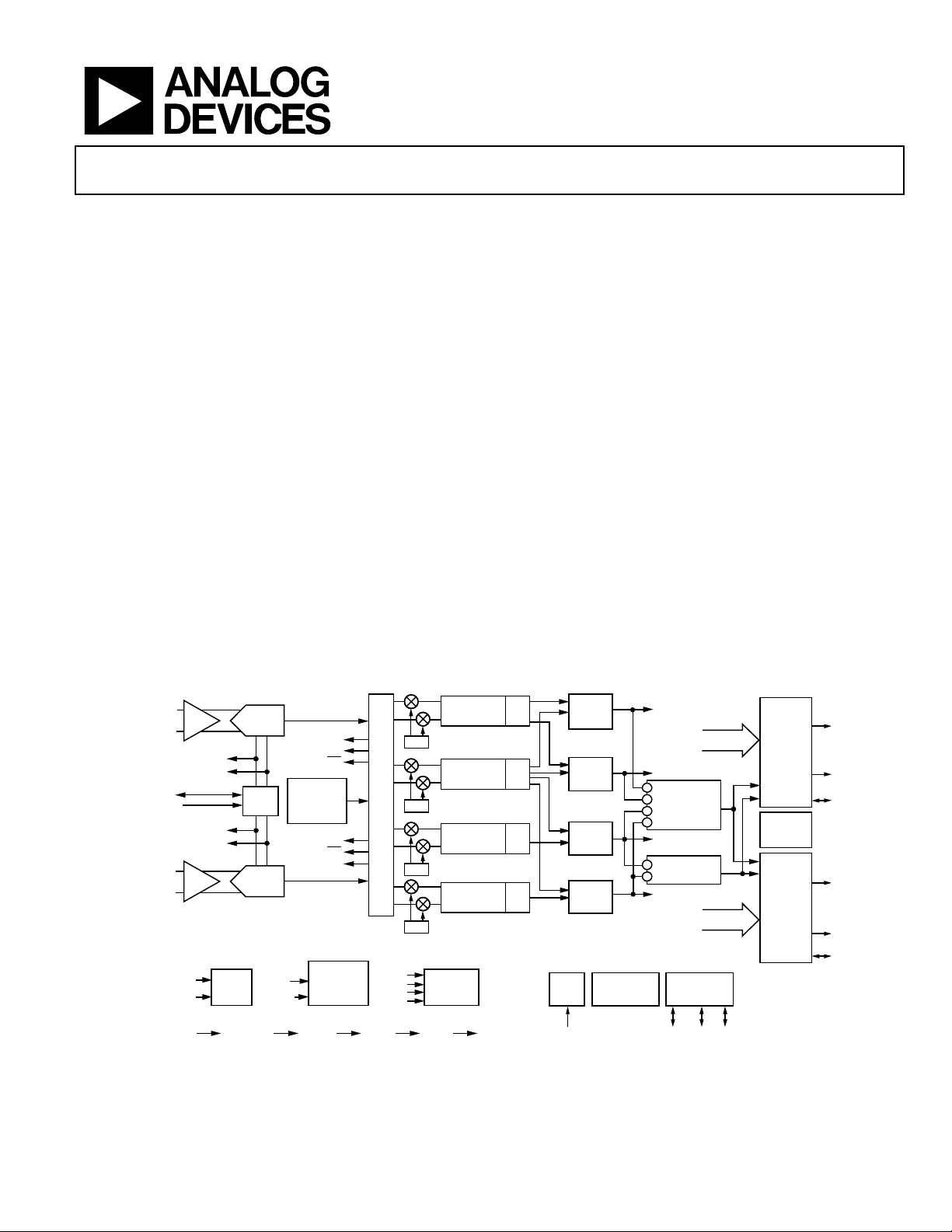
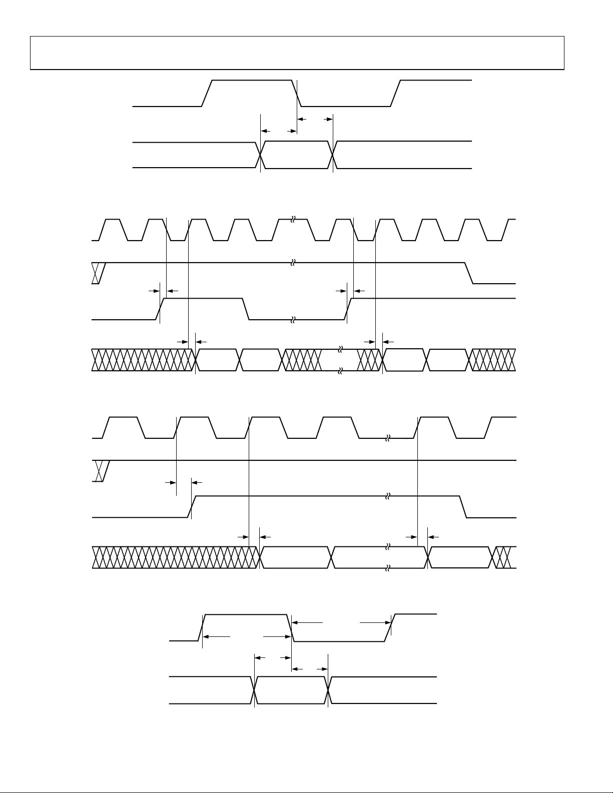
FUNCTIONAL BLOCK DIAGRAM
DUAL-CHANNEL 12-BIT A/D FRONT END WIDEBAND DIGITAL DOWNCONVERTER (DDC)
INA
SHA
–
REF
ENSE
INB+
SHA
INB–
PDWN
SHRDREF
+3.0AVDD +3.3VDDIO 2.5VDD AGND DGND
REFTA
REFBA
REFTB
REFBB
MODE
SELECT
CHANNEL
CHANNEL
ADC
A
VREF
ADC
B
ACLK
DUTYEN
12
CHANNEL A
/
OTRA
LIA
LIA
PSEUDO
RANDOM
NOISE
SEQUENCE
LIB
LIB
OTRB
12
/
CHANNEL B
CLOCK
DUTY
CYCLE
STABILIZER
INPUT MATRIX
SYNCA
SYNCB
SYNCC
SYNCD
NCO
NCO
NCO
NCO
RCIC2
RESAMPLER
RCIC2
RESAMPLER
RCIC2
RESAMPLER
RCIC2
RESAMPLER
EXTERNAL
SYNC.
CIRCUIT
IF to Baseband Diversity Receiver
AD6652
APPLICATIONS
Communications
Diversity radio systems
Multimode digital receivers:
GSM, EDGE, PHS, AMPS, UMTS, WCDMA, CDMA-ONE,
IS95, IS136, CDMA2000, IMT-2000
I/Q demodulation systems
Smart antenna systems
General-purpose software radios
Broadband data applications
Instrumentation and test equipment
CIC5
CIC5
CIC5
CIC5
*DATA INTERLEAVING AND INTERPOLATING HB FILTER
RAM
COEF.
FILTER
CHANNEL 0
RAM
COEF.
FILTER
CHANNEL 1
RAM
COEF.
FILTER
CHANNEL 2
RAM
COEF.
FILTER
CHANNEL 3
DDC
CLK
CLK DATA CONT ADD
BUILT-IN
SELF-TEST
CIRCUITRY
TO OUTPUT PORTS
CHANNELS 0, 1, 2, 3
TO OUTPUT PORTS
TO OUTPUT
PORTS
TO OUTPUT PORTS
CHANNELS 0, 1, 2, 3
Figure 1.
RCF OUTPUTS
AGC A*
AGC B*
RCF OUTPUTS
PROGRAM
MICROPORT
/
/
833
PORT A
8-BIT DSP
LINK
OR
16-BIT
PARALLEL
OUTPUT
CONTROL
OUTPUT
MUX
CIRCUITRY
PORT B
8-BIT DSP
LINK
OR
16-BIT
PARALLEL
OUTPUT
CONTROL
/
03198-0-001
Rev. 0
Information furnished by Analog Devices is believed to be accurate and reliable.
However, no responsibility is assumed by Analog Devices for its use, nor for any
infringements of patents or other rights of third parties that may result from its use.
Specifications subject to change without notice. No license is granted by implication
or otherwise under any patent or patent rights of Analog Devices. Trademarks and
registered trademarks are the property of their respective owners.
One Technology Way, P.O. Box 9106, Norwood, MA 02062-9106, U.S.A.
Tel: 781.329.4700
Fax: 781.326.8703 © 2004 Analog Devices, Inc. All rights reserved.
www.analog.com
Page 2

AD6652
TABLE OF CONTENTS
Product Description......................................................................... 4
Gain Switching............................................................................ 31
Product Highlights....................................................................... 4
Specifications..................................................................................... 5
Recommended Operating Conditions ...................................... 5
ADC DC Specifications ............................................................... 5
ADC Switching Specifications.................................................... 5
ADC AC Specifications ............................................................... 6
Electrical Characteristics ............................................................. 7
General Timing Characteristics ................................................. 8
Microprocessor Port Timing Characteristics ........................... 9
Absolute Maximum Ratings.......................................................... 10
Thermal Characteristics ............................................................10
Test Level .....................................................................................10
ESD Caution................................................................................ 10
Pin Configuration and Function Descriptions........................... 11
Typical Performance Characteristics ...........................................14
Numerically Controlled Oscillator............................................... 33
Frequency Translation to Baseband......................................... 33
NCO Shadow Register............................................................... 33
NCO Frequency Hold-Off Register......................................... 33
Phase Offset................................................................................. 33
NCO Control Register............................................................... 33
Second-Order rCIC Filter ............................................................. 35
rCIC2 Scale Factor ..................................................................... 35
rCIC2 Output Level ................................................................... 36
rCIC2 Rejection.......................................................................... 36
Decimation and Interpolation Registers ................................. 36
rCIC2 Scale Register .................................................................. 36
Fifth-Order CIC Filter ................................................................... 37
CIC5 Rejection ........................................................................... 37
RAM Coefficient Filter .................................................................. 38
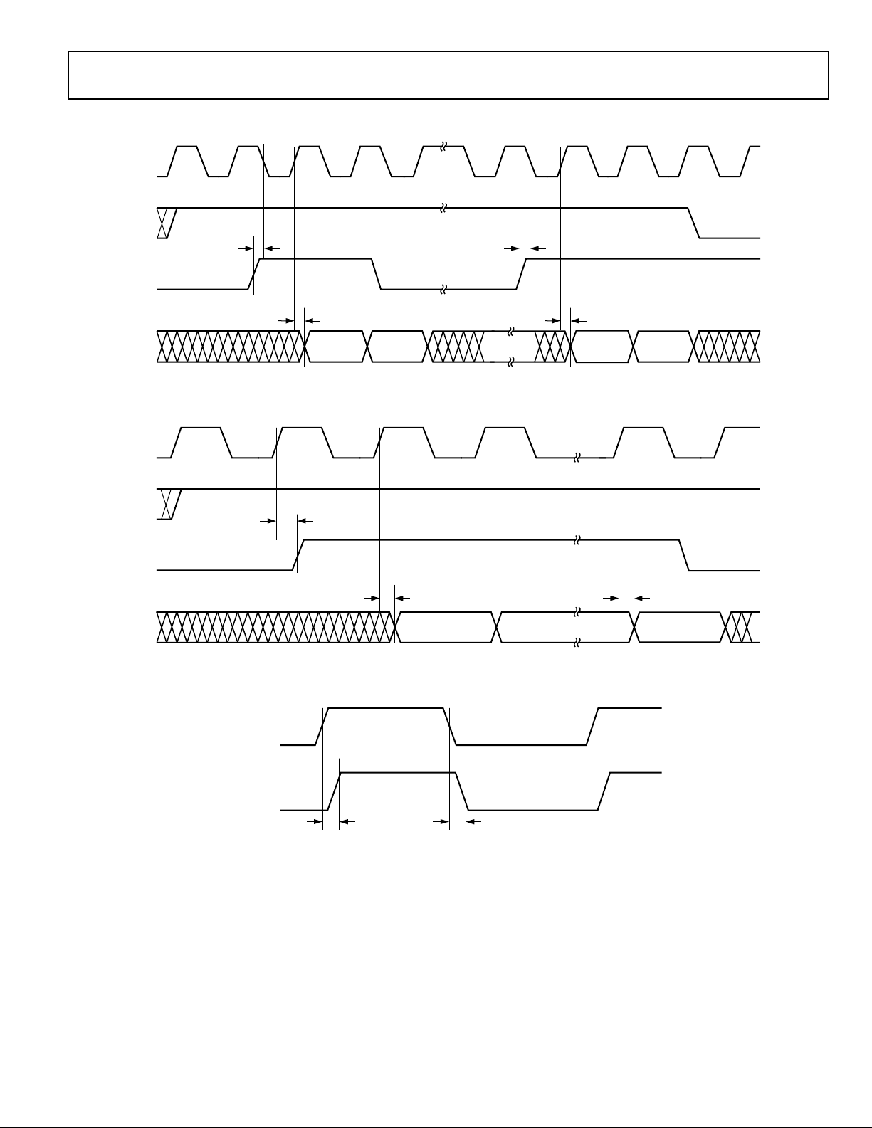
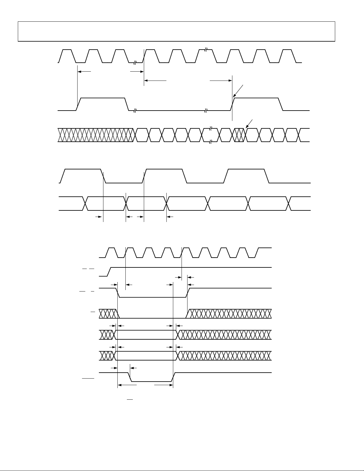
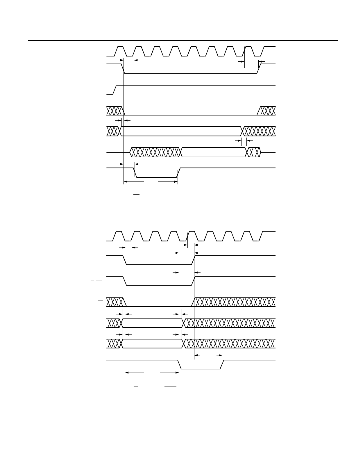
DDC Timing Diagrams .................................................................17
Terminology ....................................................................................23
ADC Equivalent Circuits........................................................... 23
Theory of Operation ...................................................................... 24
ADC Architecture ...................................................................... 24
Digital Downconverter Architecture Overview .........................29
Data Input Matrix....................................................................... 29
Numerically Controlled Oscillator...........................................29
Second-Order rCIC Filter .........................................................29
Fifth-Order CIC Filter ............................................................... 29
RAM Coefficient Filter ..............................................................29
Interpolating Half-Band Filters and AGC............................... 29
Control Register and Memory Map Address Notation .............31
DDC Input Matrix...................................................................... 31
DDC Data Latency ..................................................................... 31
RCF Decimation Register.......................................................... 38
RCF Decimation Phase.............................................................. 38
RCF Filter Length....................................................................... 38
RCF Output Scale Factor and Control Register..................... 39
Interpolating Half-Band Filters .................................................... 40
Automatic Gain Control................................................................ 41
AGC Loop ................................................................................... 41
Desired Signal Level Mode........................................................ 41
Synchronization.......................................................................... 44
User-Configurable Built-In Self-Test (BIST).............................. 45
RAM BIST................................................................................... 45
Channel BIST.............................................................................. 45
Channel/Chip Synchronization.................................................... 46
Start .............................................................................................. 46
Hop............................................................................................... 48
Rev. 0 | Page 2 of 76
Page 3

AD6652
Parallel Output Ports.......................................................................50
Pin_Sync Control Register.........................................................57
Channel Mode .............................................................................50
AGC Mode...................................................................................51
Master/Slave PCLK Modes........................................................52
Parallel Port Pin Functions ........................................................52
Link Port...........................................................................................53
Link Port Data Format ...............................................................53
Link Port Timing.........................................................................53
TigerSHARC Configuration......................................................54
External Memory Map ...................................................................55
Access Control Register (ACR).................................................56
Channel Address Register (CAR) .............................................56
Soft_Sync Control Register........................................................56
REVISION HISTORY
7/04—Revision 0: Initial Version
Sleep Control Register................................................................57
Data Address Registers...............................................................57
Channel Address Registers (CAR)............................................57
Input Port Control Registers .....................................................63
Output Port Control Registers ..................................................64
Microport Control......................................................................71
Applications .....................................................................................73
AD6652 Receiver Applications..................................................73
Design Guidelines.......................................................................73
AD6652 Evaluation Board and Software.....................................75
Outline Dimensions........................................................................76
Ordering Guide ...........................................................................76
Rev. 0 | Page 3 of 76
Page 4

AD6652
PRODUCT DESCRIPTION
The AD6652 is a mixed-signal IF to baseband receiver
consisting of dual 12-bit 65 MSPS ADCs and a wideband
multimode digital downconverter (DDC). The AD6652 is
designed to support communications applications where low
cost, small size, and versatility are desired. The AD6652 is also
suitable for other applications in imaging, medical ultrasound,
instrumentation, and test equipment.
The dual ADC core features a multistage differential pipelined
architecture with integrated output error correction logic. Both
ADCs feature wide bandwidth differential sample-and-hold
analog input amplifiers supporting a variety of user-selectable
input ranges. An integrated voltage reference eases design
considerations. A duty cycle stabilizer is provided to compensate for variations in the ADC clock duty cycle, allowing the
converters to maintain excellent performance.
ADC data outputs are internally connected directly to the
receiver’s digital downconverter (DDC) input matrix, simplifying layout and reducing interconnection parasitics. Overrange
bits are provided for each ADC channel to alert the user to
ADC clipping. Level indicator bits are also provided for each
DDC input port that can be used for external digital VGA
control.
The digital receiver has four reconfigurable channels and
provides extraordinary processing flexibility. The receiver input
matrix routes the ADC data to individual channels, or to all four
receive processing channels. Each receive channel has five
cascaded signal processing stages: a 32-bit frequency translator
(numerically controlled oscillator (NCO)), two fixed-coefficient
decimating filters (CIC), a programmable RAM coefficient
decimating FIR filter (RCF), and an interpolating half-band
filter/AGC stage. Following the CIC filters, one, several, or all
channels can be configured to use one, several, or all the RCF
filters. This permits the processing power of four 160-tap RCF
FIR filters to be combined or used individually.
After FIR filtering, data can be routed directly to the two
external 16-bit output ports. Alternatively, data can be routed
through two additional half-band interpolation stages, where up
to four channels can be combined (interleaved), interpolated,
and processed by an automatic gain control (AGC) circuit with
96 dB range. The outputs from the two AGC stages are also
routed directly to the two external 16-bit output ports. Each
output port has a 16-bit parallel output and an 8-bit link port to
permit seamless data interface with DSP devices such as the
TS-101 TigerSHARC® DSP. A multiplexer for each port selects
one of six data sources to appear on the device outputs pins.
digitizes a wide spectrum of IF frequencies and then downconverts the desired signals to baseband using individual
channel NCOs. The AD6652 provides user-configurable digital
filters for removal of undesired baseband components, and the
data is then passed on to an external DSP, where demodulation
and other signal processing tasks are performed to complete the
information retrieval process. Each receive channel is independently configurable to provide simultaneous reception of the
carrier to which it is tuned. This IF sampling architecture
greatly reduces component cost and complexity compared with
traditional analog techniques or less integrated digital methods.
High dynamic range decimation filters offer a wide range of
decimation rates. The RAM-based architecture allows easy
reconfiguration for multimode applications. The decimating
filters remove unwanted signals and noise from the channel of
interest. When the channel occupies less bandwidth than the
input signal, this rejection of out-of-band noise is referred to as
processing gain. By using large decimation factors, this processing gain can improve the SNR of the ADC by 20 dB or more. In
addition, the programmable RAM coefficient filter allows
antialiasing, matched filtering, and static equalization functions
to be combined in a single, cost-effective filter.
Flexible power-down options allow significant power savings,
when desired.
PRODUCT HIGHLIGHTS
• Integrated dual 12-bit 65 MSPS ADC.
• Integrated wideband digital downconverter (DDC).
• Proprietary, differential SHA input maintains excellent
SNR performance for input frequencies up to 200 MHz.
• Crossbar-switched digital downconverter input ports.
• Digital resampling permits noninteger relationships
between the ADC clock and the digital output data rate.
• Energy-saving power-down modes.
• 32-bit NCOs with selectable amplitude and phase dithering
for better than −100 dBc spurious performance.
• CIC filters with user-programmable decimation and
interpolation factors.
• 160-tap RAM coefficient filter for each DDC channel.
• Dual 16-bit parallel output ports and dual 8-bit link ports.
The AD6652 is part of the Analog Devices SoftCell® multimode
and multicarrier transceiver chipset. The SoftCell receiver
Rev. 0 | Page 4 of 76
• 8-bit microport for register programming, register read-
back, and coefficient memory programming.
Page 5

AD6652
SPECIFICATIONS
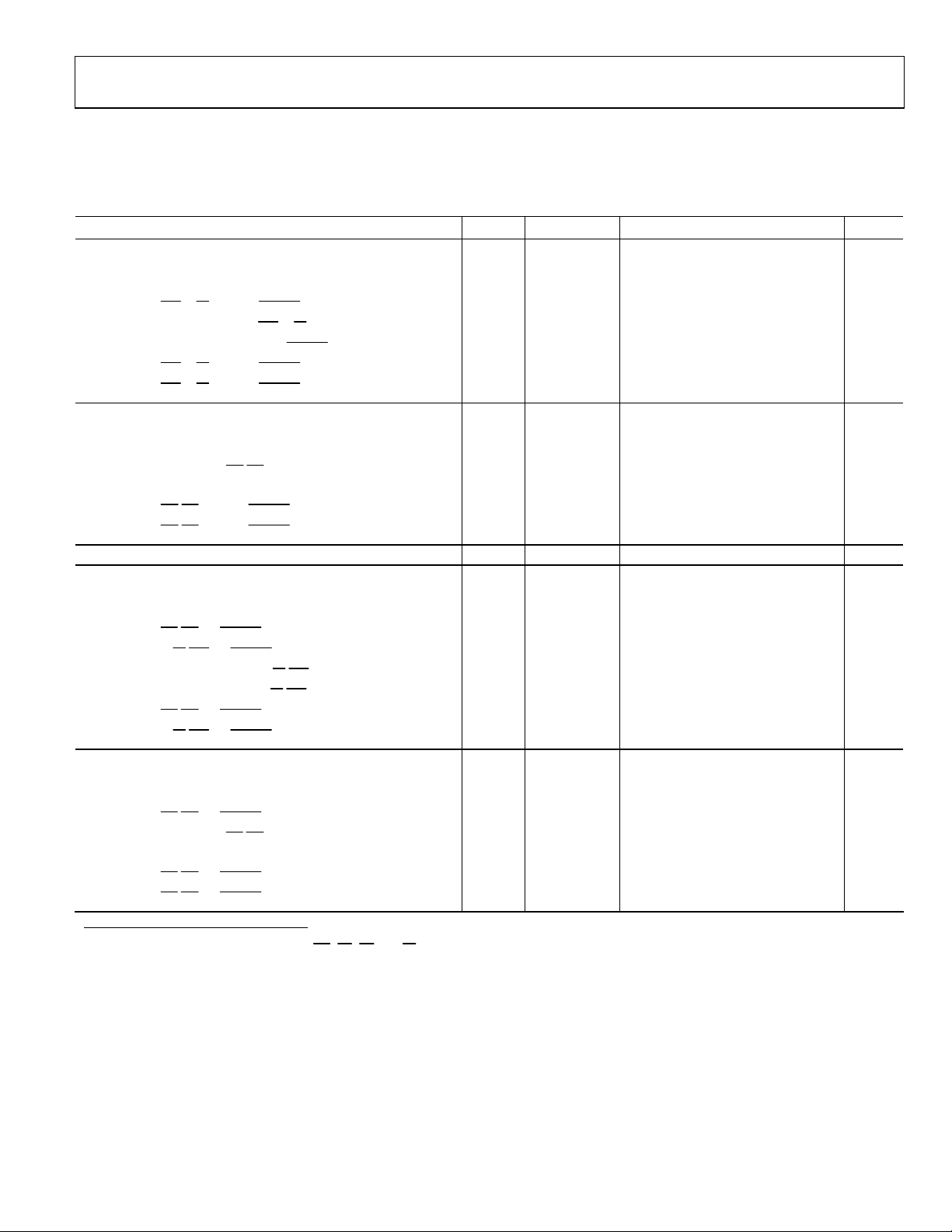
RECOMMENDED OPERATING CONDITIONS
Table 1.
Parameter Temp Test Level Min Typ Max Unit
AVDD Full IV 2.75 3.0 3.3 V
VDD Full IV 2.25 2.5 2.75 V
VDDIO Full IV 3.0 3.3 3.6 V
T
AMBIENT
ADC DC SPECIFICATIONS
AVDD = 3.0 V, VDD = 2.5 V, VDDIO = 3.3 V, 61.44 MSPS, −1.0 dBFS differential input, 1.0 V internal reference, unless otherwise noted.
Table 2.
Parameter (Conditions) Temp Test Level Min Typ Max Unit
RESOLUTION Full IV 12 Bits
INTERNAL VOLTAGE REFERENCE
Output Voltage Error (1 V Mode) Full IV ±5 ±35 mV
Load Regulation @ 1.0 mA Full V 0.8 mV
Output Voltage Error (0.5 V Mode) Full V ±2.5 mV
Load Regulation @ 0.5 mA Full V 0.1 mV
INPUT REFERRED NOISE
Input Span = 1 V Internal 25°C V 0.54 LSB rms
Input Span = 2 V Internal 25°C V 0.27 LSB rms
ANALOG INPUT
Input Span = 1.0 V Full IV 1 V p-p
Input Span = 2.0 V Full IV 2 V p-p
Input Capacitance Full V 7 pF
REFERENCE INPUT RESISTANCE Full V 7 kΩ
MATCHING CHARACTERISTICS
Offset Error Full V ±0.1 % FSR
Gain Error Full V ±0.1 % FSR
IV −40 +25 +85 °C
ADC SWITCHING SPECIFICATIONS
AVDD = 3.0 V, VDD = 2.5 V, VDDIO = 3.3 V, 61.44 MSPS, −1.0 dBFS differential input, 1.0 V internal reference, unless otherwise noted.
Table 3.
Parameter (Conditions) Temp Test Level Min Typ Max Unit
SWITCHING PERFORMANCE
Maximum Conversion Rate Full IV 65 MSPS
Minimum Conversion Rate Full V 1 MSPS
ACLK Period Full V 15.4 ns
ACLK Pulse Width High
ACLK Pulse Width Low1 Full V 6.2 ACLK/2 ns
DATA OUTPUT PARAMETERS
Wake-Up Time
2
OUT-OF-RANGE RECOVERY TIME Full V 2 Cycles
1
Duty cycle stabilizer enabled.
2
Wake-up time is dependent on the value of decoupling capacitors, typical values shown with 0.1 µF and 10 µF capacitors on REFT and REFB.
1
Full V 6.2 ACLK/2 ns
Full V 2.5 ms
Rev. 0 | Page 5 of 76
Page 6

AD6652
ADC AC SPECIFICATIONS
AVDD = 3.0 V, VDD = 2.5 V, VDDIO = 3.3 V, 61.44 MSPS, −1.0 dBFS differential input, 1.0 V internal reference.
Table 4.
Parameter (Conditions) Temp Test Level Min Typ Max Unit
SIGNAL-TO-NOISE RATIO1 (WITHOUT HARMONICS)
Analog Input Frequency 10.4 MHz 25°C V 90 dB
Full V 90 dB
25.0 MHz 25°C II 85 90 dB
Full V 90 dB
68.0 MHz 25°C II 84 89.5 dB
Full V 88.5 dB
101 MHz 25°C V 88.0 dB
150 MHz 25°C V 87.5 dB
200 MHz 25°C V 85 dB
WORST HARMONIC (2nd or 3rd)1
Analog Input Frequency 10.4 MHz 25°C V −85 dBc
Full V −83 dBc
25 MHz 25°C II −83 −71 dBc
Full V −80 dBc
68 MHz 25°C II −80 dBc
Full V −76 dBc
101 MHz 25°C V −79 dBc
150 MHz 25°C V −72 dBc
200 MHz 25°C V −69 dBc
TWO-TONE IMD REJECTION (TWO TONES SEPARATED BY 1 MHz)2
Analog Inputs = 15/16 MHz 25°C V −81 dBc
Analog Inputs = 55/56 MHz 25°C V −79 dBc
CHANNEL ISOLATION/CROSSTALK
1
Analog Input A or B = single tone @ −1 dB below full scale, 150 kHz DDC filter bandwidth.
2
Analog Input A or B = each single tone @ −7 dB below full scale, 5 MHz DDC filter bandwidth.
3
Analog Inputs A and B = each single tone @ −1 dB below full scale at 4.3 MHz and 68 MHz, 150 kHz DDC filter bandwidth.
3
Full V 85 dB
Rev. 0 | Page 6 of 76
Page 7

AD6652
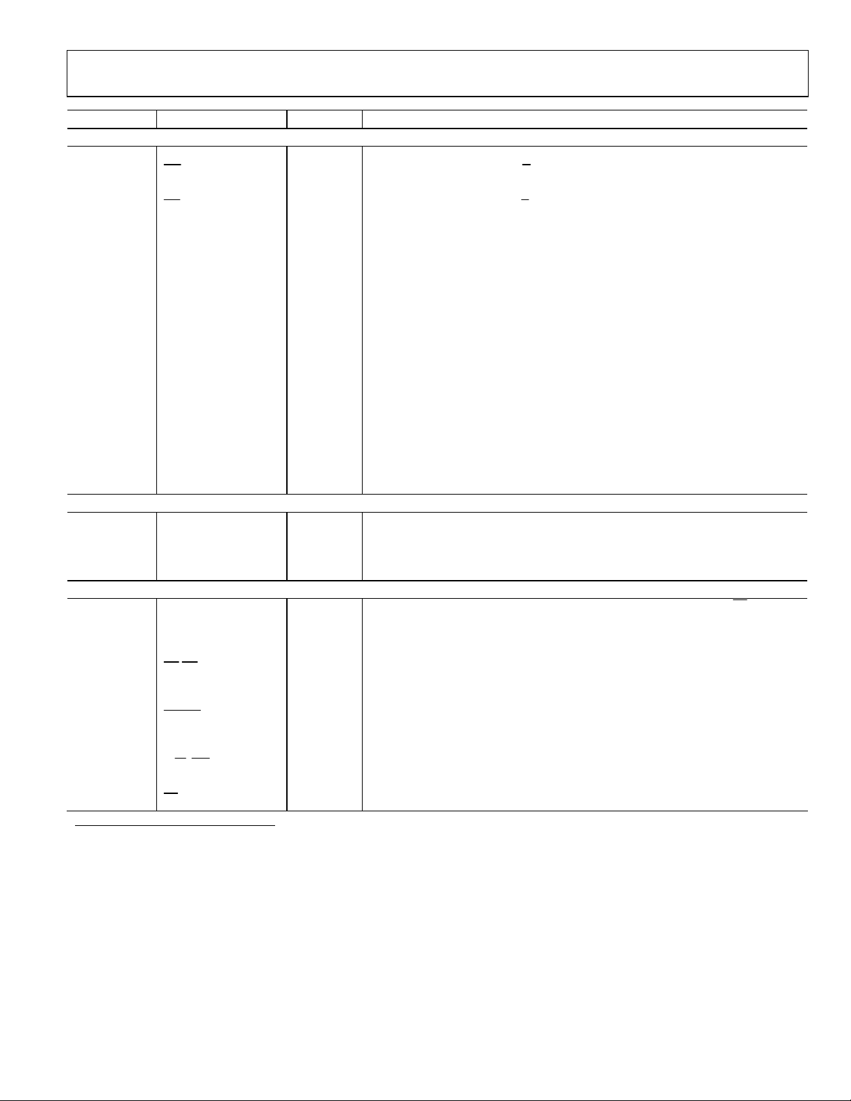
ELECTRICAL CHARACTERISTICS
AVDD = 3.0 V, VDD = 2.5 V, VDDIO = 3.3 V, 61.44 MSPS, −1.0 dBFS differential input, 1.0 V internal reference, unless otherwise noted.
Table 5.
Parameter (Conditions) Temp Test Level Min Typ Max Unit
LOGIC INPUTS
Logic Compatibility Full IV 3.3 V CMOS
Logic 1 Voltage Full IV 2.0 V
Logic 0 Voltage Full IV 0.8 V
Logic 1 Current Full IV −10 +10 µA
Logic 0 Current Full IV −10 +10 µA
Input Capacitance 25°C V 4 pF
LOGIC OUTPUTS
Logic Compatibility Full IV 3.3 V CMOS/TTL
Logic 1 Voltage (VOH) (IOH = 0.25 mA) Full IV 2.4 VDDIO − 0.2 V
Logic 0 Voltage (VOL) (IOL = 0.25 mA) Full IV 0.2 0.4 V
SUPPLY CURRENTS
Narrow Band (150 kHz BW) (61.44 MHz CLK)
Four Individual Channels
I
AVDD
I
VDD
I
VDDIO
CDMA (1.25MHz BW) (61.44 MHz CLK) Example
I
AVDD
I
VDD
I
VDDIO
1
WCDMA (5 MHz BW) (61.44 MHz CLK) Example1
I
AVDD
I
VDD
I
VDDIO
TOTAL POWER DISSIPATION
Narrow Band (150 kHz BW) (61.44 MHz CLK)
Four Individual Channels
CDMA (61.44 MHz)1
WCDMA (61.44 MHz)1
ADC in Standby and DDC in Sleep Mode
2
25°C II 160 200 215 mA
25°C II 240 280 300 mA
25°C II 25 40 45 mA
25°C V 200 mA
25°C V 336 mA
25°C V 68 mA
25°C V 200 mA
25°C V 330 mA
25°C V 89 mA
25°C II 1.2 1.5 1.6 W
25°C
25°C
25°C
V 1.7 W
V 1.7 W
V 2.3 mW
1
All signal processing stages and all DDC channels active.
2
ADC standby power measured with ACLK inactive.
Rev. 0 | Page 7 of 76
Page 8

AD6652
GENERAL TIMING CHARACTERISTICS
All timing specifications valid over VDD range of 2.25 V to 2.75 V and VDDIO range of 3.0 V to 3.6 V.
CLOAD = 40 pF on all outputs, unless otherwise specified.
Table 6.
Parameter (Conditions) Temp Test Level Min Typ Max Unit
CLK TIMING REQUIREMENTS
t
CLK
t
CLKL
t
CLKH
RESET TIMING REQUIREMENTS
t
RESL
LEVEL INDICATOR OUTPUT SWITCHING CHARACTERISTICS
t
DLI
SYNC TIMING REQUIREMENTS
t
SS
t
HS
PARALLEL PORT TIMING REQUIREMENTS (MASTER MODE)
Switching Characteristics
t
DPOCLKL
t
DPOCLKLL
t
DPREQ
t
DPP
Input Characteristics
t
SPA
t
HPA
PARALLEL PORT TIMING REQUIREMENTS (SLAVE MODE)
Switching Characteristics1
t
POCLK
t
POCLKL
t
POCLKH
t
DPREQ
t
DPP
Input Characteristics
t
SPA
t
HPA
LINK PORT TIMING REQUIREMENTS
Switching Characteristics1
t
RDLCLK
t
FDLCLK
t
RLCLKDAT
t
FLCLKDAT
1
The timing parameters for Px[15:0], PxREQ, and PxACK apply for Port A and B (x stands for A or B).
CLK Period Full IV 15.4 ns
CLK Width Low Full IV 6.2 t
CLK Width High Full IV 6.2 t
/2 ns
CLK
/2 ns
CLK
RESET Width Low
↑CLK to LI (LIA, LIA; LIB, LIB) Output Delay Time
SYNC(A,B,C,D) to ↑CLK Setup Time
SYNC(A,B,C,D) to ↑CLK Hold Time
1
↓CLK to ↑PCLK Delay (Divide-by-1)
↓CLK to ↑PCLK Delay (Divide-by-2, -4, or -8)
↑PCLK to ↑PxREQ Delay
↑PCLK to Px[15:0] Delay
PxACK to ↓PCLK Setup Time
PxACK to ↓PCLK Hold Time
Full IV 30.0 ns
Full IV 3.3 10.0 ns
Full IV 2.0 ns
Full IV 1.0 ns
Full IV 6.5 10.5 ns
Full IV 8.3 14.6 ns
1.0 ns
0.0 ns
7.0 ns
−3.0 ns
PCLK Period Full IV 12.5 ns
PCLK Low Period (when PCLK Divisor = 1) Full IV 2.0 0.5 × t
PCLK High Period (when PCLK Divisor = 1) Full IV 2.0 0.5 × t
↑PCLK to ↑PxREQ Delay
↑PCLK to Px[15:0] Delay
PxACK to ↓PCLK Setup Time
PxACK to ↓PCLK Hold Time
10.0 ns
11.0 ns
IV 1.0 ns
IV 1.0 ns
↑PCLK to ↑LxCLKOUT Delay
↓PCLK to ↓LxCLKOUT Delay
↑LCLKOUT to Lx[7:0] Delay
↓LCLKOUT to Lx[7:0] Delay
Full IV 2.5 ns
Full IV 0 ns
Full IV 0 2.9 ns
Full IV 0 2.2 ns
POCLK
POCLK
ns
ns
Rev. 0 | Page 8 of 76
Page 9
AD6652
MICROPROCESSOR PORT TIMING CHARACTERISTICS
All timing specifications valid over VDD range of 2.25 V to 2.75 V and VDDIO range of 3.0 V to 3.6 V.
CLOAD = 40 pF on all outputs, unless otherwise specified.
Table 7.
MICROPROCESSOR PORT, MODE INM (MODE = 0) Temp Test Level Min Typ Max Unit
MODE INM WRITE TIMING
t
t
t
t
t
t
t
SC
HC
HWR
SAM
HAM
DRDY
ACC
Control1 to ↑CLK Setup Time
Control1 to ↑CLK Hold Time
WR(R/W) to RDY(DTACK) Hold Time
Address/Data to WR(R/W) Setup Time
Address/Data to RDY(DTACK) Hold Time
WR(R/W) to RDY(DTACK) Delay
WR(R/W) to RDY(DTACK) High Delay
MODE INM READ TIMING
t
t
t
t
t
t
SC
HC
SAM
HAM
DRDY
ACC
Control1 to ↑CLK Setup Time
Control1 to ↑CLK Hold Time
Address to RD(DS) Setup Time
Address to Data Hold Time Full IV 5.0 ns
RD(DS) to RDY(DTACK) Delay
RD(DS) to RDY(DTACK) High Delay
MICROPROCESSOR PORT, MODE MNM (MODE = 1) Temp Test Level Min Typ Max Unit
MODE MNM WRITE TIMING
t
SC
t
HC
t
HDS
t
HRW
t
SAM
t
HAM
t
DDTACK
t
ACC
Control1 to ↑CLK Setup Time
Control1 to ↑CLK Hold Time
DS(RD) to DTACK(RDY) Hold Time
R/W(WR) to DTACK(RDY) Hold Time
Address/Data To R/W(WR) Setup Time
Address/Data to R/W(WR) Hold Time
DS(RD) to DTACK(RDY) Delay
R/W(WR) to DTACK(RDY) Low Delay
MODE MNM READ TIMING
t
SC
t
HC
t
HDS
t
SAM
t
HAM
t
DDTACK
t
ACC
Control1 to ↑CLK Setup Time
Control1 to ↑CLK Hold Time
DS(RD) to DTACK(RDY) Hold Time
Address to DS(RD) Setup Time
Address to Data Hold Time Full IV 5.0 ns
DS(RD) to DTACK(RDY) Delay
DS(RD) to DTACK(RDY) Low Delay
Full IV 2.0 ns
Full IV 2.5 ns
Full IV 7.0 ns
Full IV 3.0 ns
Full IV 5.0 ns
Full IV 8.0 ns
Full IV 4 × t
CLK
5 × t
CLK
9 × t
CLK
ns
Full IV 5.0 ns
Full IV 2.0 ns
Full IV 0.0 ns
Full IV 8.0 ns
Full IV 8 × t
CLK
10 × t
CLK
13 × t
CLK
ns
Full IV 2.0 ns
Full IV 2.5 ns
Full IV 8.0 ns
Full IV 7.0 ns
Full IV 3.0 ns
Full IV 5.0 ns
Full IV 8.0 ns
Full IV 4 × t
CLK
5 × t
CLK
9 × t
CLK
ns
Full IV 5.0 ns
Full IV 2.0 ns
Full IV 8.0 ns
Full IV 0.0 ns
Full IV 8.0 ns
Full IV 8 × t
CLK
10 × t
CLK
13 × t
CLK
ns
1
Specification pertains to control signals: R/W, (WR), DS, (RD), and CS.
Rev. 0 | Page 9 of 76
Page 10

AD6652
ABSOLUTE MAXIMUM RATINGS
Table 8.
Parameter Rating
ELECTRICAL
AVDD Voltage −0.3 V to +3.9 V
VDD Voltage −0.3 V to +2.75 V
VDDIO Voltage −0.3 V to +3.9 V
AGND, DGND −0.3 V to +0.3 V
ADC VINA, VINB Analog Input Voltage −0.3 V to AVDD + 0.3 V
ADC Digital Input Voltage −0.3 V to AVDD + 0.3 V
ADC OTRA, OTRB Digital Output Voltage
ADC VREF, REFA, REFB Input Voltage −0.3 V to AVDD + 0.3 V
DDC Digital Input Voltage −0.3 V to VDDIO + 0.3 V
DDC Digital Output Voltage −0.3 V to VDDIO + 0.3 V
ENVIRONMENTAL
Operating Temperature Range
(Ambient)
Maximum Junction Temperature
Under Bias
Storage Temperature Range (Ambient) −65°C to +150°C
−0.3 V to VDDIO + 0.3 V
−40°C to +85°C
150°C
Stresses above those listed under the Absolute Maximum
Ratings may cause permanent damage to the device. This is a
stress rating only; functional operation of the device at these or
any other conditions above those indicated in the operational
section of this specification is not implied. Exposure to absolute
maximum rating conditions for extended periods may affect
device reliability.
THERMAL CHARACTERISTICS
256-lead CSPBGA, 17 mm sq.
= 23°C/W, still air.
θ
JA
Estimate based on JEDEC JC51-2 model using horizontally
positioned 4-layer board.
TEST LEVEL
I. 100% production tested.
II.
100% production tested at 25°C.
III. Sample tested only.
IV. Parameter guaranteed by design and characterization testing.
V. Parameter is a typical value only.
VI.
100% production tested at 25°C; guaranteed by design and
characterization testing for industrial temperature range.
ESD CAUTION
ESD (electrostatic discharge) sensitive device. Electrostatic charges as high as 4000 V readily accumulate on
the human body and test equipment and can discharge without detection. Although this product features
proprietary ESD protection circuitry, permanent damage may occur on devices subjected to high energy
electrostatic discharges. Therefore, proper ESD precautions are recommended to avoid performance
degradation or loss of functionality.
Rev. 0 | Page 10 of 76
Page 11
AD6652
PIN CONFIGURATION AND FUNCTION DESCRIPTIONS
Table 9. BGA Pin Configuration (Top View)
1 2 3 4 5 6 7 8 9 10 11 12 13 14 15 16
DGND PA7_LA7 A2 PA6_LA6 D1 D3
A
Do Not
Connect
PA4_LA4
B
PA9 PA3_LA3 A1
C
PA1_LA1 PA2_LA2
D
PA8 PA5_LA5 n.c. VDD VDD VDD VDD VDDIO VDDIO VDDIO VDDIO VDDIO AVDD AVDD AGND AGND
E
PA0_LA0 DGND PA10 DGND DGND DGND DGND DGND DGND DGND DGND VDDIO AVDD AGND AGND AGND
F
PA12 PA11 PA13 DGND DGND DGND DGND DGND DGND DGND DGND VDDIO AVDD AGND REFBB REFTB
G
PAR EQ PA 15 PA1 4 DGND DGND DGND DGND DGND DGND DGND DGND VDDIO AVDD AGND AGND SENSE
H
CHIP_ID1 DGND DGND DGND DGND DGND DGND DGND DGND DGND DGND VDDIO AVDD AGND AGND VREF
J
CHIP_ID3 PAACK CHIP_ID0 DGND DGND DGND DGND DGND DGND DGND DGND VDDIO AVDD AGND REFBA REFTA
K
PB6_LB6 PB7_LB7 DGND DGND DGND DGND DGND DGND DGND DGND DGND VDDIO AVDD AGND AGND AGND
L
PAC H0 _
LACLK
OUT
PAC H1 _
LACLKIN
A0
DS (RD
VDD VDD VDD VDD VDDIO VDDIO VDDIO VDDIO VDDIO AVDD AVDD AGND VI N−B
DGND
D0 D2 D5 D7
)
R/
CS RESE T
W (WR
D4 D6 SYNCC SYNCA LIA DUTYEN
)
MODE SYNCD OTRA PDWN AVDD AVDD AGND AGND
DTACK
(RDY)
SYNCB
LIA
AVDD AVDD AGND AGND
LIB AVDD AVDD AGND VIN+B
CHIP_ID2 PB3_LB3 PB4_LB4 VDDIO VDDIO VDDIO VDDIO VDD VDD VDD VDD VDDIO AVDD AVDD AG ND AGND
M
PAI Q
N
P
PBIQ
R
DGND PCLK PB5_ LB5 PB11 PB13 PBREQ n.c. n.c. n.c. n.c. DCLK SHRDREF AVDD ACLK AGND AGND
T
PBCH1_
LBCLK IN
DGND PB0_LB0 PB8 PB10 PB14 VDDIO PBACK
PBCH0_L
BCLKOUT
PB2_LB2
PB1_ LB1 PB9 PB12 PB15 n.c. n.c. n.c. n.c. n.c. PDWN
VDDIO VDDIO VDDIO VDDIO VDD VDD VDD VDD VDDIO AVDD AVDD AGND VI N−A
LIB
n.c. n.c. OTRB n.c. AVDD AVDD AGN D VIN+A
AVDD AVDD AGND AGND
Rev. 0 | Page 11 of 76
Page 12

AD6652
Table 10. Pin Function Descriptions
Pin No. Mnemonic Type Function
POWER SUPPLY
A13, B13, C13, D13, E13, F13, G13, H13, J13, K13, L13, M13, N13, P13, R13,
T13, A14, B14, C14, D14, E14, M14, N14, P14, R14
D4, D5, D6, D7, E4, E5, E6, E7, M8, M9, M10, M11, N8, N9, N10, N11 VDD Power 2.5 V Digital Core Supply, 16 Pins.
D8, D9, D10, D11, D12, E8, E9, E10, E11, E12, F12, G12, H12, J12, K12, L12,
M4, M5, M6, M7, M12, N4, N5, N6, N7, N12, P6
A1, B5, F2, F4, F5, F6, F7, F8, F9, F10, F11, G4, G5, G6, G7, G8, G9, G10, G11,
H4, H5, H6, H7, H8, H9, H10, H11, J2, J3, J4, J5, J6, J7, J8, J9, J10, J11, K4,
K5, K6, K7, K8, K9, K10, K11, L3, L4, L5, L6, L7, L8, L9, L10, L11, P1, T1
A15, A16, B15, B16, C15, D15, E15, E16, F14, F15, F16, G14, H14, H15, J14,
J15, K14, L14, L15, L16, M15, M16, N15, P15, R15, R16, T15, T16
MISCELLANEOUS
E3, P9, P10, P12, R7, R8, R9, R10, R11, T7, T8, T9, T10 NC N/A No Connect, 13 Pins.
B1 DNC N/A Do Not Connect.
Pin No. Mnemonic Type Function
ADC INPUTS
P16 VIN+A Input Differential Analog Input Pin (+) for Channel A.
N16 VIN−A Input Differential Analog Input Pin (−) for Channel A.
C16 VIN+B Input Differential Analog Input Pin (+) for Channel B.
D16 VIN−B Input Differential Analog Input Pin (−) for Channel B.
J16 VREF I/O Voltage Reference Input/Output.
H16 SENSE Input Voltage Reference Mode Select.
T14 ACLK Input ADC Master Clock.
B12 DUTYEN Input Duty Cycle Stabilizer, Active High.
A12, R12 PDWN
1
Input Power-Down Enable, Active High.
T12 SHRDREF Input Shared Voltage Reference Select, Low = Independent, High = Shared.
ADC OUTPUTS
A11 OTRA Output Out-of-Range Indicator for Channel A, High = Overrange.
P11 OTRB Output Out-of-Range Indicator for Channel B, High = Overrange.
K16 REFTA Output Top Reference Voltage, Channel A.
G16 REFTB Output Top Reference Voltage, Channel B.
K15 REFBA Output Bottom Reference Voltage, Channel A.
G15 REFBB Output Bottom Reference Voltage, Channel B.
DDC INPUTS
A8
RESET
Input Master Reset, Active Low.
T11 DCLK Input DDC Master Clock.
T2 PCLK I/O Link Port Clock Output or Parallel Port Clock Input.
D3 PACH1_LACLKIN
2
I/O
Channel ID Output Bit, MSB, for Parallel Port A, or Link Port A Data Ready Input.
Function depends on logic state of 0x1B:7 of output port control register.
N2 PBCH1_LBCLKIN2 I/O
Channel ID Output Bit, MSB, for Parallel Port B, or Link Port B Data Ready Input.
Function depends on logic state of 0x1D:7 of output port control register.
B10 SYNCA
3
Input Hardware Sync, Pin A, Routed to All Receiver Channels.
C10 SYNCB3 Input Hardware Sync, Pin B, Routed to All Receiver Channels.
B9 SYNCC3 Input Hardware Sync, Pin C, Routed to All Receiver Channels.
A10 SYNCD3 Input Hardware Sync, Pin D, Routed to All Receiver Channels.
3
K3, J1, M1,
K1
CHIP_ID[3:0]
Input
Chip ID Selector, Four Pins, Used in Conjunction with Access Control Register
Bits 5–2.
AVDD Power 3.0 V Analog Supply, 25 Pins.
VDDIO Power 3.3 V Digital I/O Supply, 27 Pins.
DGND Ground Digital Ground, 56 Pins.
AGND Ground Analog Ground, 28 Pins.
Rev. 0 | Page 12 of 76
Page 13
AD6652
Pin No. Mnemonic Type Function
DDC OUTPUTS
B11 LIA Output Level Indicator, Input A, Data A.
C11
LIA
C12 LIB Output Level Indicator, Input B, Data B.
P8
LIB
B3 PACH0_LACLKOUT2 Output
R2 PACH0_LBCLKOUT2 Output
F1, D1, D2,
PA[7:0]_LA[7:0] Output Link Port A Data or Parallel Port A Data [7:0], Eight Pins.
C2, B2, E2,
A4, A2
P2, R3, N3,
PB[7:0_LB[7:0] Output Link Port B Data or Parallel Port B Data [7:0], Eight Pins.
M2, M3, T3,
L1, L2
E1, C1, F3,
PA[15:8] Output Parallel Port A Data [15:8], Eight Pins.
G2, G1, G3,
H3, H2
P3, R4, P4,
PB[15:8] Output Parallel Port B Data [15:8], Eight Pins.
T4, R5, T5,
P5, R6
N1 PAIQ Output Parallel Port A I or Q Data Indicator, I = High, Q = Low.
R1 PBIQ Output Parallel Port B I or Q Data Indicator, I = High, Q = Low.
PARALLEL OUTPUT PORT CONTROL
K2 PAACK Input Parallel Port A Acknowledge.
H1 PAREQ Output Parallel Port A Request.
P7 PBACK Input Parallel Port B Acknowledge.
T6 PBREQ Output Parallel Port B Request.
MICROPORT CONTROL
C5, A5, C6,
D[7:0] I/O
A6, B7, C7,
B8, C8
B4, C3, A3 A[2:0] Input Microport Address Bus, 3 Pins.
C4
C9
B6
4
DS(RD)
DTACK(RDY)
W (WR)4
R/
4, 5
A9 MODE4 Input Mode Select Pin. 0 = Intel mode, 1 = Motorola mode.
A7
CS3
Output
Output
Level Indicator, Input A, Data
Level Indicator, Input B, Data
A.
B.
Channel ID Output Bit, LSB, for Parallel Port A, or Link Port A Clock Output.
Function depends on logic state of 0x1B:7 of output port control register.
Channel ID Output Bit, LSB, for Parallel Port B, or Link Port B Clock Output.
Function depends on logic state of 0x1D:7 of output port control register.
Bidirectional Microport Data, Eight Pins. This bus is three-stated when CS is high.
Input Function depends upon MODE pin.
Active Low Data Strobe when MODE = 1.
Active Low Read Strobe when MODE = 0.
Output Function depends upon MODE pin.
Active Low Data Acknowledge when MODE = 1.
Microport Status Pin when MODE = 0.
Input Read/Write Strobe when MODE = 1. Active Low Write strobe when MODE = 0.
Input Active Low Chip Select. Logic 1 three-states the microport data bus.
1
PDWN pins must be the same logic level: both logic high or both logic low.
2
PACH0 and PACH1 form a 2-bit output word in the parallel output mode that identifies the processing channel (0, 1, 2, or 3) whose data appears on Port A parallel
outputs. Likewise, PBCH0 and PBCH1 identify the channel for Port B.
3
Pins with a pull-down resistor of nominal 70 kΩ.
4
Mode 0 is Intel nonmultiplexed (IMN), and Mode 1 is Motorola nonmultiplexed (MNM). Pin logic level corresponds to mode.
5
Pins with a pull-up resistor of nominal 70 kΩ.
Rev. 0 | Page 13 of 76
Page 14
AD6652
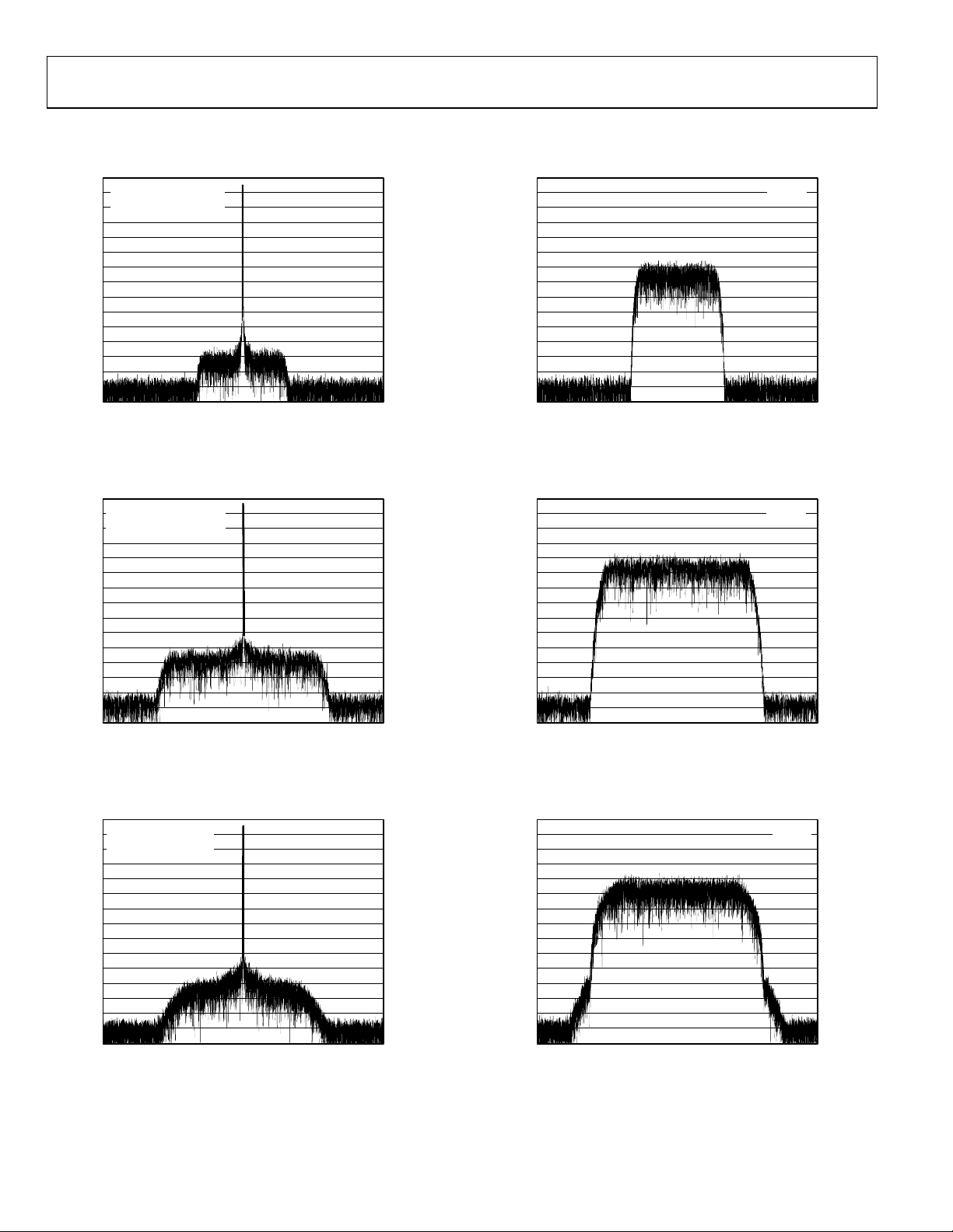
TYPICAL PERFORMANCE CHARACTERISTICS
0
AIN = –1dBFS
–10
SNR = 90dB (200kHz BW)
–20
32k FFT
–30
–40
–50
–60
–70
–80
dBFS
–90
–100
–110
–120
–130
–140
–150
–300 –200 –100 0 100 200 300
FREQUENCY (kHz)
Figure 2. GSM/EDGE with Single Tone A
= 30 MHz; Encode = 61.44 MSPS
IN
0
AIN = –1dBFS
–10
SNR = 80dB (1.25MHz BW)
–20
32k FFT
–30
–40
–50
–60
–70
–80
dBFS
–90
–100
–110
–120
–130
–140
–150
–1.2 –0.8 –0.4 0 0.4 0.8 1.2
FREQUENCY (MHz)
Figure 3. CDMA2000 with Single Tone A
= 76 MHz; Encode = 61.44 MSPS
IN
0
AIN = –1dBFS
–10
SNR = 70dB (5MHz BW)
–20
32k FFT
–30
–40
–
50
–60
–70
–80
dBFS
–90
–100
–110
–120
–130
–140
–150
Figure 4. WCDMA with Single Tone A
–101234–3 –2–4
FREQUENCY (MHz)
= 169 MHz; Encode = 61.44 MSPS
IN
03198-0-060
03198-0-062
03198-0-064
0
–10
–20
–30
–40
–50
–60
–70
–80
dBFS
–90
–100
–110
–120
–130
–140
–150
–300 –200 –100 0 100 200 300
FREQUENCY (kHz)
Figure 5. GSM/EDGE Carrier A
= 30 MHz; Encode = 61.44 MSPS
IN
0
–10
–20
–30
–40
–50
–60
–70
–80
dBFS
–90
–100
–110
–120
–130
–140
–150
–1.2 –0.8 –0.4 0 0.4 0.8 1.2
FREQUENCY (MHz)
Figure 6. CDMA2000 Carrier A
= 76 MHz; Encode = 61.44 MSPS
IN
0
–10
–20
–30
–40
–50
–60
–70
–80
dBFS
–90
–100
–110
–120
–130
–140
–150
Figure 7. WCDMA Carrier A
–101234–3 –2–4
FREQUENCY (MHz)
= 169 MHz; Encode = 61.44 MSPS
IN
32k FFT
32k FFT
32k FFT
03198-0-059
03198-0-061
03198-0-063
Rev. 0 | Page 14 of 76
Page 15
AD6652
0
ENCODE = 61.44MSPS
–10
A
IN
–20
32k FFT
–30
–40
–50
–60
–70
–80
dBFS
–90
–100
–110
–120
–130
–140
–150
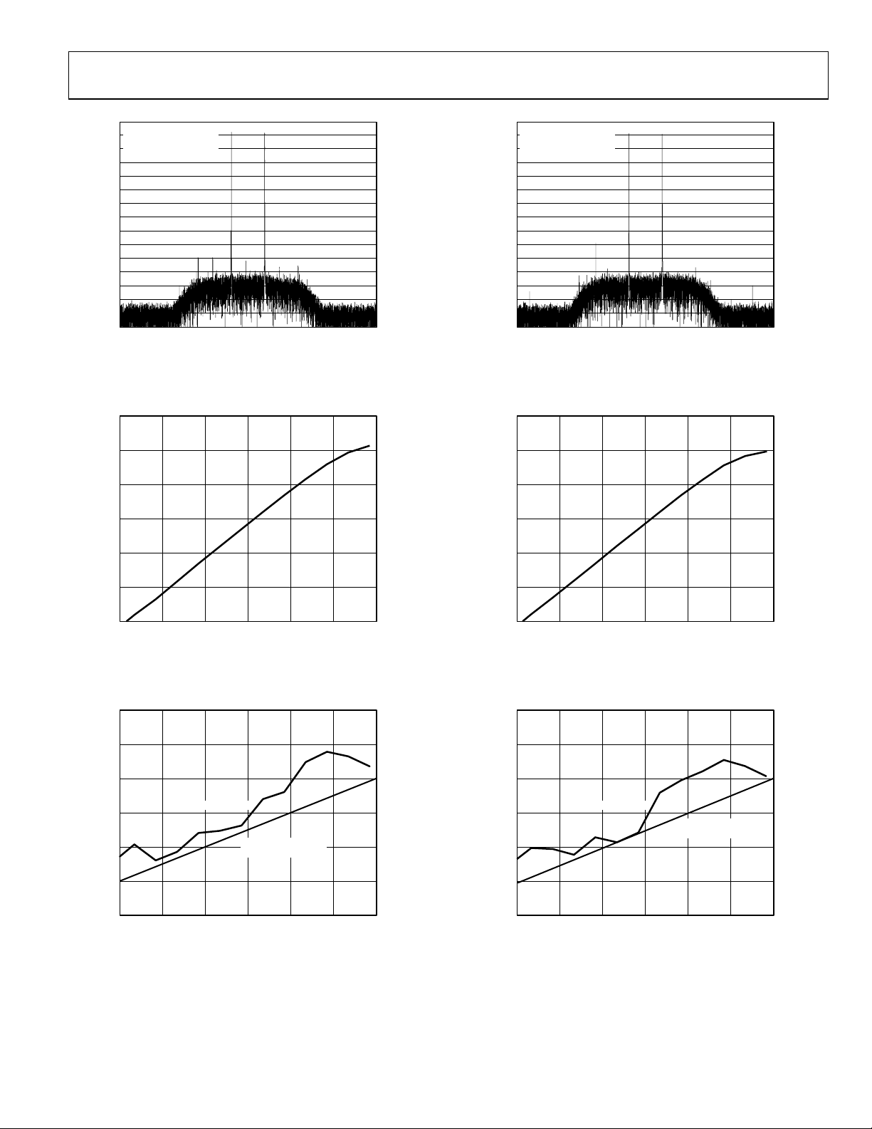
100
= –7dBFS
–101234–3 –2–4
FREQUENCY (MHz)
Figure 8. Two Tones at 15 MHz and 16 MHz
03198-0-070
0
ENCODE = 61.44MSPS
–10
A
IN
–20
32k FFT
–30
–40
–50
–60
–70
–80
dBFS
–90
–100
–110
–120
–130
–140
–150
100
= –7dBFS
–101234–3 –2–4
FREQUENCY (MHz)
Fig z ure 11. Two Tones at 55 MHz and 56 MH
03198-0-066
90
80
70
60
SNR (dB) [150kHz BW]
50
40
SNR
–40 –30–60 –50 –20 –10 0
ANALOG INPUT AMPLITUDE (dBFS)
03198-0-071
Figure 9. Noise vs. Analog Amplitude at 25 MHz
100
90
80
70
60
HARMONICS (dBc)
HARMONICS
HARMONICS = 80dB
REFERENCE LINE
90
80
70
60
SNR (dB) [150kHz BW]
50
40
SNR
–40 –30–60 –50 –20 –10 0
ANALOG INPUT AMPLITUDE (dBFS)
03198-0-072
Figure 12. Noise vs. Analog Amplitude at 68 MHz
100
90
80
70
60
HARMONICS (dBc)
HARMONICS
HARMONICS = 80dB
REFERENCE LINE
50
40
–40 –30–60 –50 –20 –10 0
ANALOG INPUT AMPLITUDE (dBFS)
Figure 10. Harmonics vs. Analog Amplitude at 25 MHz
03198-0-073
Rev. 0 | Page 15 of 76
50
40
–40 –30–60 –50 –20 –10 0
ANALOG INPUT AMPLITUDE (dBFS)
Figure 13. Harmonics vs. Analog Amplitude at 68 MHz
03198-0-074
Page 16
AD6652
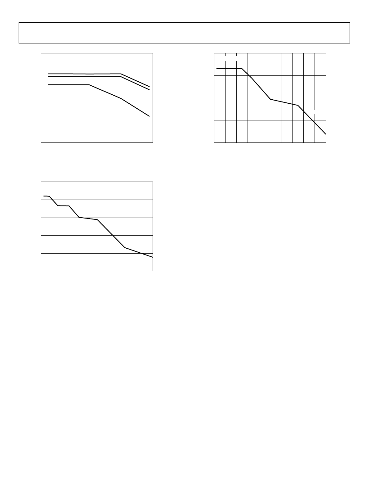
92
AIN = –1dBFS
92
AIN = –1dBFS
25°C
90
= 150kH
88
SNR (dB) [BW z]
86
0 10203040506070
ANALOG INPUT FREQUENCY (MHz)
85°C
–40°C
Figure 14. Noise vs. Analog Frequency
90
AIN = –1dBFS
85
80
25°C
75
03198-0-068
90
88
SNR (dB) [BW = 150kHz]
86
84
0 20 40 60 80 100 120 140 160 180 200
ANALOG INPUT FREQUENCY (MHz)
Figure 16. Noise vs. Analog Frequency (IF)
25°C
03198-0-067
70
WORST-CASE HARMONIC (dBc)
65
75 100 125 150 175 20025 500
ANALOG FREQUENCY (MHz)
03198-0-069
Figure 15. Harmonics vs. Analog Frequency
Rev. 0 | Page 16 of 76
Page 17
AD6652
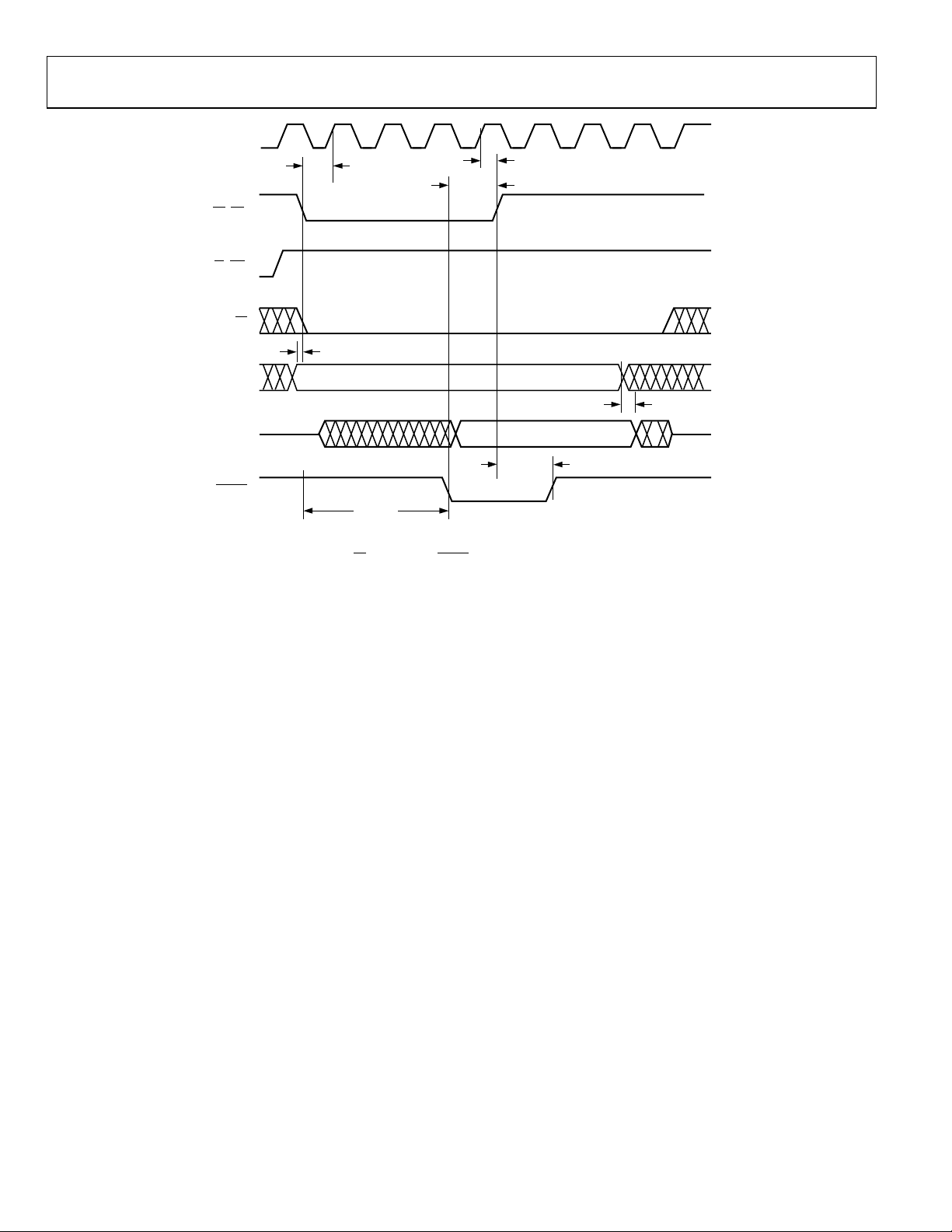
K
K
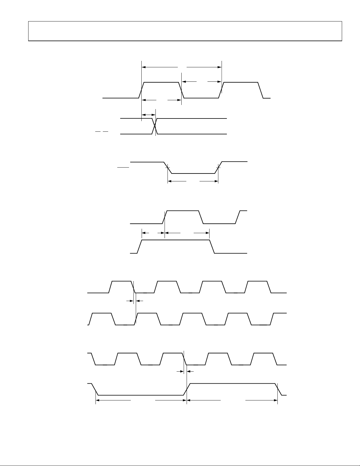
DDC TIMING DIAGRAMS
t
CLK
t
CLKL
CL
t
CLKH
t
DLI
LIA, LIB
LIA, LIB
03198-0-065
Figure 17. Level Indicator Output Switching Characteristics
RESET
t
RESL
03198-0-003
Figure 18. Reset Timing Requirements
CLK
t
HS
03198-0-006
SYNCA
SYNCB
SYNCC
SYNCD
t
SS
Figure 19. SYNC Timing Inputs
CLK
t
DPOCLKL
PCL
03198-0-007
Figure 20. PCLK to CLK Switching Characteristics Divide-by-1
CLK
t
DPOCLKLL
PCLK
t
POCLKH
t
POCLKL
03198-0-008
Figure 21. PCLK to CLK Switching Characteristics Divide-by-2, -4, or -8
Rev. 0 | Page 17 of 76
Page 18
AD6652
K
PCLK
PxREQ
PxACK
PCLK
PxACK
t
HPA
t
SPA
03198-0-009
Figure 22. Master Mode PxACK to PCLK Setup and Hold Characteristics
t
SPA
t
SPA
Px[15:0]
t
DPP
DATA 1 DATA 2 DATA N – 1 DATA N
t
DPP
03198-0-010
Figure 23. Master Mode PxACK to PCLK Switching Characteristics
PCLK
PxACK
t
DPREQ
PxREQ
Px[15:0]
t
DPP
DATA 1 DATA N
t
DPP
03198-0-011
Figure 24. Master Mode PxREQ to PCLK Switching Characteristics
t
PCLK
t
POCLKH
POCLKL
t
SPA
PxAC
t
HPA
03198-0-012
Figure 25. Slave Mode PxACK to PCLK Setup and Hold Characteristics
Rev. 0 | Page 18 of 76
Page 19
AD6652
PCLK
PxREQ
PxACK
t
SPA
t
SPA
Px[15:0]
t
DPP
DATA 1 DATA 2 DATA N – 1 DATA N
t
DPP
03198-0-013
Figure 26. Slave Mode PxACK to PCLK Switching Characteristics
PCLK
PxACK
t
DPREQ
PxREQ
Px[15:0]
t
DPP
DATA 1 DATA N
t
DPP
03198-0-014
Figure 27. Slave Mode PxREQ to PCLK Switching Characteristics
PCLK
LxCLKOUT
t
RDLCLK
t
FDLCL
03198-0-015
Figure 28. LxCLKOUT to PCLK Switching Characteristics
Rev. 0 | Page 19 of 76
Page 20
AD6652
LxCLKOUT
LxCLKIN
WAIT ≥ 6 CYCLES
ONE TIME CONNECTIVITY CHECK
8 LxCLKOUT CYCLES
NEXT TRANSFER
ACKNOWLEDGE
NEXT TRANSFER
BEGINS
Lx[7:0]
LxCLKOUT
Lx[7:0]
CLK
RD (DS)
WR (R/W)
Figure 29. LxCLKIN to LxCL
t
FDLCLKDAT
Figure 30. LxCLKOUT to Lx
t
SC
D0
D1
t
RDLCLKDAT
D2 D3 D4 D15 D3
KOUT Data witching Characteristics
S
D0 D1 D2
[7:0] Data Switching Characteristics
t
HC
t
HWR
03198-0-016
03198-0-017
CS
t
t
HAM
HAM
03198-0-018
A[2:0]
D[7:0]
RDY
(DTACK)
t
SAM
VALID ADDRESS
t
SAM
LID DATA
VA
t
DRDY
t
ACC
NOTES
1.
t
ACCESS TIME DEPENDS ON THE ADDRESS ACCESSED. ACCESS TIME IS MEASURED
ACC
FROM FE OF WR TO RE OF RDY.
t
REQUIRES A MAXIMUM OF 9 CLK PERIODS.
2.
ACC
Figure 31. INM Microport Write Timing Requirements
Rev. 0 | Page 20 of 76
Page 21
AD6652
CLK
t
RD (DS)
WR (RW)
CS
SC
t
SAM
t
HC
A[2:0]
D[7:0]
RDY
(DTACK)
t
DRDY
NOTES
1.
t
ACCESS TIME DEPEND
ACC
FROM FE OF WR TO RE OF RDY.
t
REQUIRES A MAXIMUM OF 13
2.
ACC
VALID ADDRESS
t
ACC
S ON THE ADDRESS
CLK PERIOD
t
HA
VALID DATA
ACCESSED. ACCESS TIME IS MEASURED
S.
03198-0-019
iming Requirements Figure 32. INM Micropor t Read T
CLK
t
HC
DS (RD)
RW (WR)
t
SC
t
HDS
t
HRW
CS
t
HAM
t
HAM
t
ACC
HE FE OF DTACK.
XIMUM OF 9 CLK PERIODS.
THE ADDRESS ESS TIME IS MEASURED
ort Write Timing Requirements
t
DDTACK
ACCESSED. ACC
03198-0-020
A[2:0]
D[7:0]
DTACK
(RDY)
t
SAM
VALID ADDRESS
t
SAM
NOTES
t
ACCESS TIME DEPENDS ON
1.
ACC
FROM FE OF DS TO T
2.
t
REQUIRES A MA
ACC
Figure 33. MNM Microp
VALID DATA
Rev. 0 | Page 21 of 76
Page 22
AD6652
CLK
DS (RD)
R/W (WR)
CS
A[2:0]
t
t
SC
t
HDS
t
SAM
HC
VALID ADDRESS
t
HA
D[7:0]
DTACK
(RDY)
t
ACC
NOTES
1.
t
ACCESS TIME DEPENDS ON T
ACC
FROM THE FE OF DS TO THE FE O
t
REQUIRES A MAXIMUM OF 13
2.
ACC
HE ADDRESS ACC
F DTACK.
CLK PERIOD
S.
Timing Requirements Figure 34. MNM Microport Read
VALID DATA
t
DDTACK
ESSED. ACCESS TIME IS MEASURED
03198-0-021
Rev. 0 | Page 22 of 76
Page 23
AD6652
TERMINOLOGY
Crosstalk
Coupling onto one channel being driven by a (−0.5 dBFS) signal
when the adjacent interfering channel is driven by a full-sc
ale
signal. Measurement includes all spurs resulting from both
direct coupling and mixing components.
IF Sampling (Undersampling)
Due to the effects of aliasing, an ADC is not necessarily limited
to Nyquist sampling. Frequencies above Nyquist are aliased and
appear in the first Nyquist zone (dc to Sample Rate/2). Care
must be taken to limit the bandwidth of the sampled signal so
that it does not overlap Nyq
sam y the bandwidth of the input
pling performance is limited b
HA (sample-and-hold amplifier) and clock jitter. (Jitter adds
S
uist zones and alias onto itself. IF
more noise at higher input frequencies.)
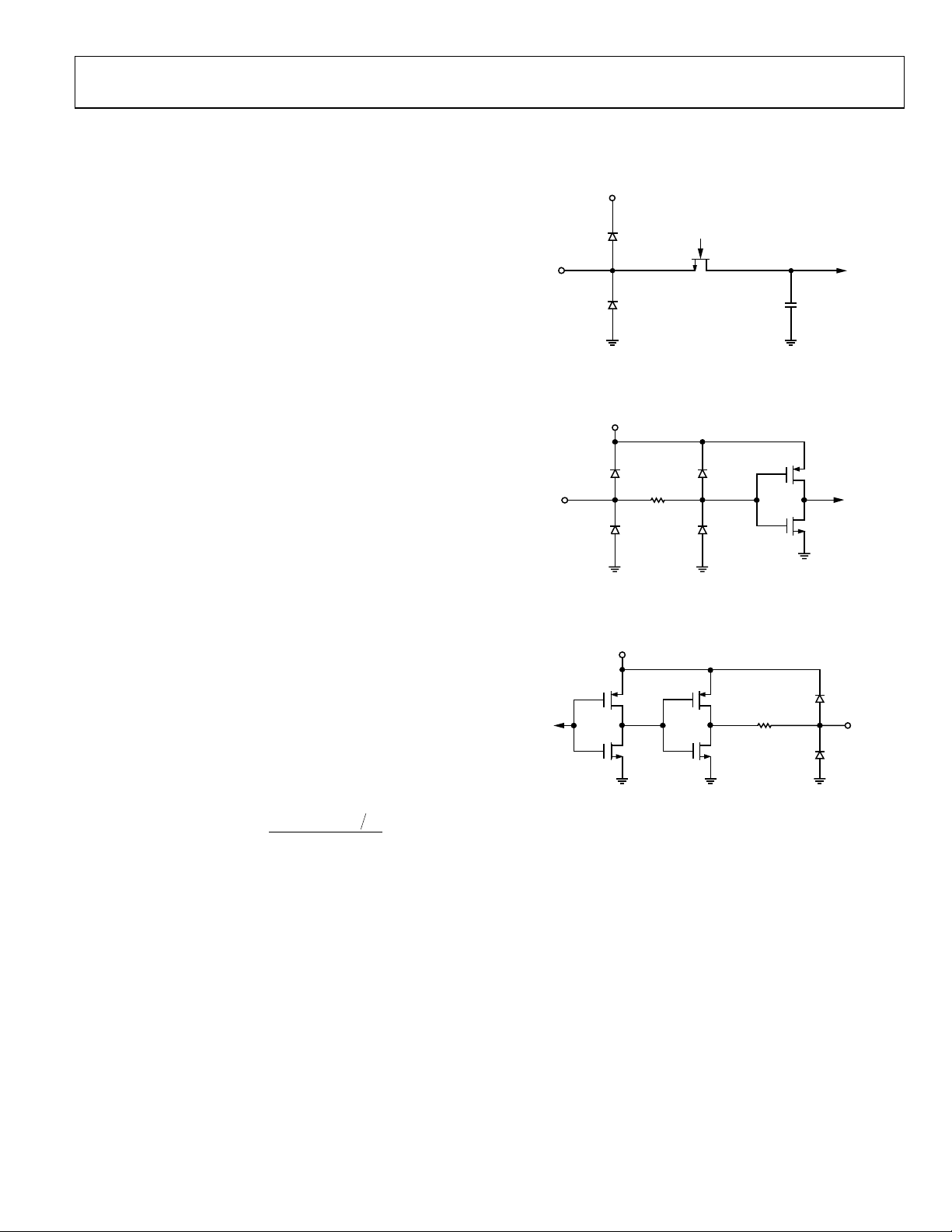
ADC EQUIVALENT CIRCUITS
AVDD
Figure 35. Analog Input Circuit
AVDD
03198-0-022
Nyquist Samplin ling)
Oversampling occu frequen f the
analog input signal are be e Nyqu
and requires that the analo ut frequency b at least
g (Oversamp
rs when the cy components o
low th ist frequency (F
g inp e sampled
/2),
clo
ck
two samples per cycle.
ut-of-Range Recovery Time
O
Out-of-range recovery time is th time it takes for the analogto-digital co after a
transient fro ove
nverter (ADC) to reacquire the analog input
m 10% above positive full scale to 10% ab
e
negative full scale, or from 10% below negative full scale to 10%
below positive full scale.
Processing Gain
When the tuned channel occupies less bandwidth than the
input signal, this rejection of out-of-band noise is referred to as
processing gain. By using large decimation factors, this processing gain can improve the SNR of the ADC by 20 dB or more.
The following equation can be used to estimate processing gain:
RateSample
2_
=
_GainProcessing
⎡
log10
⎢
⎣
BandwidthFilter
_
⎤
⎥
⎦
Signal-to-Noise Ratio (SNR)
The ratio of the rms value of the measured input signal to the
rms sum of all other spectral components within the programmed DDC filter bandwidth, excluding the first six
harmonics
cibels (dB).
de
and dc. The value for SNR is expressed in
03198-0-023
Figure 36. Digital Input
VDD
03198-0-024
Figure 37. Digital Output
Two -Ton e I MD Rejection
The ratio of the rms value of either input tone to the rms value
of the worst third-order intermodulation product; reported
in dBc.
Rev. 0 | Page 23 of 76
Page 24

AD6652
THEORY OF OPERATIO
The AD6652 has two analog input channels, four digital filtering channels, and two digital output channels. The IF input
signal passes through several stages before it appears at th
output port(s) as a well-filtered, decimated digital baseba
signal:
•
12-bit A/D conversio
•
Frequency translation from IF to baseband using
quadrature mixers and NCOs
•
Second-order resampling decimating CIC FIR filter
(rCIC2)
•
Fifth-order decimating CIC FIR filter (CIC5)
•
RAM coefficient decimating FIR filter (RCF)
•
Automatic gain control (AGC)
•
2× interpolation and channel interleave
Any stage can be bypassed with the exception of the ADC f
end. Any combination of processing channels can be combined
or interleaved after the R
filtering objectives that are not possible with just one channel.
In the following sections, each st ge is examined to allow the
user to f
The dual ADC design is useful for diversity reception of signals,
where the ADCs are operating identically on the same carrier
but from two separate antennae. The ADCs can also be
operated with independent analog inputs. The user can sample
any fs/2 frequency segment from dc to 100 MHz using
appropriate low-pass or band-pass filtering at the ADC inputs
with little loss in ADC performance. Operation to 200 MHz
analog input is permitted, but at the expense of increased ADC
distortion.
In nondiversity applications, up to four GSM/EDGE-type
carriers can be concurrently processed from the ADC stage.
Wideband signals, such as WCDMA/CDMA2000, require the
power of two AD6652 processing channels per carrier to
adequately remove adjacent channel interference. When
diversity techniques a er of carriers that
can be processed is halv ocessing requirement of diversity reception.
Flexi
(D
one output port. Four synch
frequency hop, and AGC functions to be precisely orchestr
with other devices. The NCO’s phase can be set to produce a
known offset relative to another channel or device.
ully utilize the AD6652’s capabilities.
ble channel multiplexing in the digital downconverter
DC) stage allows one to four channels to be interleaved onto
n
CF stages to achieve demanding
re employed, the numb
ed due to the dual pr
N
e
nd
ront
a
ronization input pins allow startup,
ated
ADC ARCHITECTU
The AD6652 front-end consists of two high performance, 12-bit
ADCs, preceded by differential sample-and-hold amplifiers
(SHA) that provide excellent SNR performance from dc to
200 MHz. A flexible, integrated voltage reference allows analog
inputs up to 2 V p-p. Each channel is equipped with an
overrange pin that toggles high whenever the analog input
exceeds the upper or lower reference voltage boundary. ADC
outputs are internally routed to the input matrix of the DDC
stage for channel distribution. The ADC data outputs are not
directly accessible to the user.
Each sample-and-hold amplifier (SHA) is followed by a pipelined switched capacitor ADC. The pipelined ADC is divided
into three sections, consisting of a 4-bit first stage followed by
eight 1.5-bit stages and a final 3-bit flash. Each stage provides
sufficient overlap to correct for flash errors in the preceding
stages. The quantized outputs from each stage are combined
into a final 12-bit result in the digital correction logic. The
pipelined architecture permits the first stage to operate on a
new input sample while the remaining stages operate on the
preceding samples. Sampling occurs on the rising edge of the
clock.
RE
Analog Input Operation
The analog inputs to the AD6652 are differential switched
capacitor SHAs that have been designed for optimum performance while processing differential input signals. The AD6652
accepts inputs over a wide common-mode range; however, an
input common-mode voltage V
recommended to maintain optimal performance and to
minimize signal-dependent errors.
Referring to Figure 38, the clock signal alternatively switches the
SHA between sample mode and hold mode. When the SHA is
switched into sample mode, the signal source must be capable
of charging the sample capacitors and settling within one-half
of a clock cycle. A small resistor in series with each input can
help reduce the peak transient current required from the output
stage of the driving source. Also, a small shunt capacitor can be
placed across the inputs to provide dynamic charging currents.
This passive network creates a low-pass filter at the ADC’s
input; therefore, the precise values are dependent upon the
application. In IF undersampling applications, any shunt capacitors should be removed. In combination with the driving source
impedance, the shunt capacitors would limit the input
bandwidth.
, one-half of AVDD, is
CM
Programming and control of the AD6652 is accomplished using
an 8-bit parallel interface.
Rev. 0 | Page 24 of 76
Page 25

AD6652
e source impedances driving For best dynamic performance, th
the differential analog inputs should be matched such that
common-mode settling errors are symmetrical. These errors are
reduced by the common-mode rejection of the ADC.
H
S
VINA+
S
VINA–
Figure 38. Switched-Capacitor SHA Input for One ADC Channel
5pF
S = SAMPLE
H = HOLD
5pF
S
S
H
03198-0-025
The SHA should be driven from a source that keeps the signal
peak e
s within the allowable range for the selected referenc
voltage. m put
The minimum and maximum common- ode in
levels are defined as follows:
VCM
VCM
The minimum common-mode input level allows the AD66
= VREF/2
MIN
= (AV D D + VREF)/2
MAX
52 to
accommodate ground-referenced inputs.
This is especially true in IF undersampling applications in
which input frequencies in the range of 70 MHz to 200 MHz are
being sampled. For these applications, differential transform
coupling is the recommended input configuration, as shown i
Figure 39. Transforme
ratio broadband RF transfor
r T1 is a center-tapped, 1:4 impedance
mer. The signal characteristics must
be considered when selecting a transformer. Most RF
transformers saturate at frequencies below a few MHz, and
excessive signal power can also cause core saturation, which
leads to distortion.
AVDD
VINA
AD6652
VINB
AGND
1V p-p
Figure 39. Differential AC-
49.9Ω
T1
Coupled Input for One Channel of the AD6652
1kΩ
1kΩ0.1µF
50Ω
10pF
50
10pF
Ω
ADC Voltage Reference
A stable and accurate 0.5 V voltage reference is built into the
AD6652. The input span of the ADC tracks reference voltage
changes linearly. An internal differential reference buffer creates
positive and negative reference voltages, REFT and REFB,
respectively, that define the span of the ADC core. The output
common mode of the reference buffer is set to midsupply, and
the REFT and REFB voltages and span are defined as follows:
er
n
03198-0-028
Although optimum performance is achieved with a differ
put, a single-ended source can be driven into VIN+ or VIN−.
in
n this configuration, one input accepts the signal, while the
I
ential
opposite input should be set to midscale by connecting it to an
appropriate reference. For example, a 2 V p-p signal can be
applied to VIN+, while a 1 V reference is applied to VIN−. The
AD6652 then accepts a signal varying between 2 V and 0 V. In
the single-ended configuration, distortion performance might
degrade significantly, compared to the differential case.
However, the effect is less noticeable at lower analog input
frequencies.
Differential Input Configurations
Optimum performance is achieved while driving the AD6652
inputs in a differential input configuration. For baseband
applications to Nyquist, the AD8138 Differential Driver
provides excellent performance and a flexible interface to the
ADC The output common-mode voltage of the AD8138 is
easily set to one-half of AVDD, and the driver can be configured
in a Sallen-Key filter topology to provide band limiting of the
input signal.
At input frequencies above Nyquist, the performance of most
amplifiers is not adequate to achieve the true performance of
the AD6652 ADC stage.
1/2 (AV D D + VREF)
REFT =
REFB = 1/2 (AV D D − VREF)
Span = 2 × (REFT − REFB) = 2 × VREF
As shown by the equations above, the REFT and REFB voltages
are symmetrical about the midsupply voltage and, by definition,
the input span is twice the value of the VREF voltage. Proper
operation of the AD6652 requires that VREF be no less than
0.5 V and no greater than 1.0 V.
The internal voltage reference can be pin-strapped to fixed
values of 0.5 V or 1.0 V, or adjusted within the same range, as
discussed in the Internal Reference Connection section. Maximum SNR performance is achieved with the reference set to the
largest input span of 2 V p-p. The relative SNR degradation is
3 dB when changing from 2 V p-p mode to 1 V p-p mode.
If operation using an external reference voltage is desired, it can
be substituted for the internal reference, as detailed in the
External Reference Operation section.
Rev. 0 | Page 25 of 76
Page 26

AD6652
0
Internal Reference Connection
A comparator within the AD6
SENSE pin and configures t
652 detects the potential at the
he reference into four possible
states, which are summarized in Table 11. If SENSE is grounde
d,
In all referen
conversion core and establish its in
the ADC always equals twice the v
either an internal or an external reference.
the reference amplifier switch is connected to the internal
resistor divider (see Figure 40), setting VREF to a FIXED 1 V
reference output. Connecting the SENSE pin directly to V
REF
switches the reference amplifier output to the SENSE pin,
completing the loop and providing a fixed 0.5 V reference
output. If a resistor divider is connected, as shown in Figure 41,
the switch is again set to the SENSE pin. This puts the reference
amplifier in a noninverting mode with the VREF programmab
le
The reference amplifier switch is located near the bottom left.
The SENSE pin is shown connected to ground, which sets VREF
to 1 V. Decoupling capacitors must be duplicated for the
Channel B ADC core, if it is used. The Channel B ref amp an
ADC core are identical to those of Channel A, but a
shown.
output defined as follows:
VREF = 0.5 × (1 + R2/R1)
Table 11. Reference SENSE Operation
Selected Mode SENSE Voltage Resu (V) Resulting Differential Span (V p-p)
lting VREF
External Reference AVDD External Reference 2 × External Reference
Internal Fixed Reference VREF 0.5 1.0
Programmable Reference 0.2 V to VREF 0.5 × (1 + R2/R1) 2 × VREF (See Figure 42)
Internal Fixed Reference AGND to 0.2 V 1.0 2.0
ce configurations, REFT and REFB drive the A/D
put span. The input range of
oltage at the reference pin for
d
re not
.1µF
VINA+
VINA–
CH A
ADC
CORE
0.5V
VREF
10µF
SENSE
R
R
INT
INT
TO CH B
REF AMP
SELECT
LOGIC
REF
AMP A
VREF
Figure 40. Fixed Internal Reference Configuration
REFT_A
0.1µF
REFB_A
0.1µF
0.1µF
10µF
03198-0-029
0.1 F
µ
VINA+
VINA–
REF
AMP A
R
R
INT
INT
TO CH B
REF AMP
SELECT
LOGIC
VREF
WHERE R1 + R2 =
10kΩ TO 20kΩ
10µF
R2
R1
VREF
SENSE
Figure 41. Programmable Reference Configuration
CH A
ADC
CORE
0.5V
REFT_A
REFB_A
0.1µF
0.1µF
0.1µF
10µ
F
03198-0-030
Rev. 0 | Page 26 of 76
Page 27

AD6652
External Reference Operation
An external reference voltage can be used to enhance the gain
accuracy of the ADC or improve thermal drift characteristics.
When multiple ADCs track one another, a single reference
(internal or external) might be necessary to reduce gainmatching errors to an acceptable level. A high-precision
external reference can also be selected to provide lower gain and
offset temperature drift.
When the SENSE pin is tied to AVDD as in Figure 42, the
internal reference is disabled, allowing the use of an external
reference. An internal reference buffer loads the external
reference with an equivalent 7 kΩ load. The internal buffer still
generates the positive and negative full-scale references, REFT
and REFB, for the ADC core. The input span is always twice the
value of the reference voltage; therefore, the external reference
must be limited to a maximum of 1 V.
If the internal reference of the AD6652
s, the loading on VREF by the other converters must be
IC
onsidered. Figure 44 shows how the internal reference voltage
c
is used to drive multiple
is affected by loading.
VINA+
0.5V TO 1.0V
EXTERNAL
REFERENCE IN
0.1µF
VINA–
CH A
ADC
CORE
10µF
SENSE
+3.0V
VREF
R
R
INT
INT
TO CH B
REF AMP
SELECT
LOGIC
REF
AMP A
VREF
Figure 42. External Reference Operation with Connections
Shown for Channel A Only
REFT_A
0.1µF
0.1µF
10µF
REFB_A
0.1µF
0.5V
03198-0-031
1.2
1.0
V
= 1V
REF
0.8
= 0.5V
V
0.6
ERROR (%)
REF
V
0.4
0.2
0
–40 –30 –20 –10 0 20 6010 30 40 50 70 80 90
TEMPERATURE (°C)
REF
Figure 43. Typical VREF Drift
0.05
0
–0.05
–0.10
RROR (%)
E
–0.15
–0.20
–0.25
1V ERROR
1.0 1.50 0.5 2.0 2.5 3.0
LOAD (mA)
0.5V ERROR
Figure 44. VREF Accuracy vs. Load
Shared Reference Mode
The shared reference mode allows the user to connect the
references from the dual ADCs together for superior gain and
offset matching performance. If the ADCs are to function
independently, the reference decoupling should be treated
independently and can provide superior isolation between the
dual ADC channels. To enable shared reference mode, the
SHRDREF pin must be tied high and the differential references
must be externally shorted together, that is, REFTA must be
shorted externally to REFTB and REFBA must be shorted
externally to REFBB.
03198-0-075
03198-0-076
Rev. 0 | Page 27 of 76
Page 28

AD6652
Clock Input Considerations
Typical high speed ADCs use both clock edges to generate a
variety of internal timing signals, and as a result can be sensiti
to ACLK clock duty cycle. Commonly a 5% tolerance is
required on the clock duty cycle to maintain dynamic performance characteristics. The AD6652 contains a clock duty cycle
stabilizer that re-times the nonsampling edge, providing a
internal clock signal
b
sta ilizing is engaged by setting DUTYEN to logic high. This
w
allo s a wide range of ACLK clock input duty cycles without
affec
ting the performance of the AD6652 ADC stage.
e
Th duty cycle stabilizer uses a delay-locked loop (DLL) to
crea
te the nonsampling edge. As a result, any changes to the
sam low
pling frequency require approximately 2 ms to 3 ms to al
the quire and lock to the new rate.
DLL to ac
gh
Hi speed, high resolution ADCs are sensitive to the quality of
the c
lock input. The degradation in SNR at a given full-scale
inpu f
t frequency (
with a nominal 50% duty cycle. Duty cycle
) due only to aperture jitter (tA) can be
INPUT
calculated with the following equation:
SNR degradation = 20 × log10 [1/2 × p × f
In the equation, the rms aperture jitter, t
, represents the root-
A
INPUT
× tA]
sum square of all jitter sources, which include the clock inpu
analog input signal, and ADC aperture jitter specification.
Undersampling applications are particularly sensitive to jitter.
To minimize clock jitter, treat the ACLK clock input as an
analog signal. Power supplies for clock drivers should be
separated from the ADC output driver supplies to avoid
ve
n
t,
modulating the clock
crystal-controlled osci
signal with digital noise. Low jitter,
llators make the best clock sources. If the
ACLK clock is generated from another type of source (by
gating, dividing, or other methods), re-time it by the origi
clock at the tep.
last s
nal
ADC Power-Down Mode
e power dissip d by the AD6652 front-end AD is propor-
Th ate C
nal to its samp g rate. Norma DC operation uires that
tio lin l A req
th PDWN pin e set to logic lo he ADC can placed in
bo s b w. T be
a p od th o lo
ower-down m e by setting bo PDWN pins t gic high.
w power dissi ion in power-d n mode is ach ed by
Lo pat ow iev
shu e r two
tting down th eference buffers and biasing ne rks of
bo els down e d
th ADC chann . Both power- pins must b riven
tog igh pe ion
ether either h or low for pro r ADC operat .
Fo ow AC g in
r maximum p er savings, the LK and analo put(s)
ould remain st while in stan mode, result in a
sh atic dby ing
typ nsum W If t
ical power co ption of 1 m for the ADC. he clock
inp tive dby
uts remain ac while in stan mode, typical power
co th .
nsumption for e ADC is 12 mW
ADC Wake-Up Time
The deco
when entering standby mo
upling capacitors on REFT and REFB are discharged
de, and then must be recharged when
returning to normal operation. As a result, the wake-up time is
related to the time spent in standby mode. Shorter standby
cycles result in proportionally shorter wake-up times. With
recommended 0.1 µF and 10 µF deco
REFB, it takes approximately 1 s to full
and y discharge the
referenc
operatio
e buffer decoupling capacitors, and 5 ms to restore full
n.
upling capacitors on REFT
the
Rev. 0 | Page 28 of 76
Page 29

AD6652
DIGITAL DOWNCONVERTER ARCHITE RVIEW
DATA INPUT MATRIX
The digital downconverter (DDC) section features dual high
speed 12-bit input ports that are capable of crossbar multiplexing of data to the four processing channels that follow the inpu
matrix. In addition, a third input option to the matrix is
available to facilitate BIST (built-in self-test). This option is a
pseudorandom noise (PN) sequence. The dual input ports
permit diversity reception of a carrier, or they can be treated as
unrelated and independent inputs. Either input port or the P
sequence can be routed to any or all four tuner channels. This
flexibility allows up to four signals to be processed simultane
ously. Refer to the DDC Input Matrix section for a
complete description.
NUMERICALLY CONTROLLED OSCILLATOR
Frequency translation is accomplished with a 32-bit complex
numerically controlled oscillator (NCO). Each of the four
processing channels contains a separate NCO. Real data
entering this stage is separated
(Q) components. This stage translates the input signal from a
digital intermediate frequency (IF) to digital baseband. Phase
and amplitude dither can be enabled on-chip to improve
spurious performance of the NCO. A phase-offset word is
available to create a known phase relationship between multiple
AD6652s or between channels.
SECOND-ORDER rCIC FILTER
Following frequency translation is a resampling, fixed
coefficient, high s g cascade
integrator comb (rCIC2) filter, which reduces the sample rate
based on the ratio between the decimation and interpolation
registers. The resampler allows for noninteger relationships
etween the master clock and the output data rate. This stage
b
can be bypassed by setting the decimation/interpolation ratio
to 1.
peed, second-order, resamplin
FIFTH-ORDER CIC FILTER
The next stage is a fifth-order cascaded integrator comb (CIC5)
filter, whose response is defined by the decimation rate. The
purpose of these filters is to reduce the data rate to the final
filter stage and to provide antialias filtering. The reduced data
rate allows the RAM coefficient filter (RCF) stage to calculate
more taps per output.
into in-phase (I) and quadrature
CTURE OVE
more
N
-
RAM COEFFICIENT FILTER
The RAM coefficient filter (RCF) stage is a sum-of-products
FIR filter with programmable 20-bit coefficients, and decima-
t
tion rates programmable from 1 to 256 (1 to 32 in practice).
Each RAM coefficient FIR filter (RCF in Figure 1) can handle
maximum of 160 taps. Two or more RCF stages can be combined using flexible channel configuration to increase the
processing powe
The RCF outputs of each channel can be directly routed to one
or both output ports or to an AGC stage, where selected DDC
channels can be interleaved and interpolated in a half-band
filter, if desired.
INTERPOLATING HALF-BAND FILTERS AND AGC
Processed RCF data can also be routed to two half-band
interpolation stages, where up to four channels can be
combined (interleaved), interpolated by a factor of two, and
automatic gain control (AGC) applied. Each AGC stage ha
dynamic range of 96.3 dB. These stages can be bypassed
independently of each other. The outputs from the two AGC
stages are routed to both output port multiplexers. Each outpu
has a link port to permit seamless data interface with DSP
devices such as the T
selects one of the six data sources to appear at the device
parallel or link output pins.
The overall filter response for the AD6652 is the composite o
all decimating and interpolating stages. Each successive filter
stage is capable of narrower transition bandwidths, but requires
a greater number of CLK cycles to calculate the output. Mor
decimation in the first filter stage helps to minimize overal
power consumption.
Figure 45 illustrates the basic function of the AD6652, that is, to
select and filter a single carrier from a wide input spectrum and
to down-convert it to baseband data. Figure 46 shows examples
of the combined filter response of the rCIC2, CIC5, and RCF for
narrowband and wideband carriers.
a
r beyond the 160 tap maximum.
s a
t
igerSHARC. A multiplexer for each port
f
e
l
Rev. 0 | Page 29 of 76
Page 30

AD6652
–
–
f
/2
S
f
/2 3
S
20
0
–20
–40
dBc
–60
–80
–100
–120
–1.53 104–1.03 10
(–
f
/2 TO +
f
WIDEBAND INPUT SPECTRUM
SIGNAL OF INTEREST IMAGE SIGNAL OF INTEREST
–f
f
/8 –5
S
f
/8 –5
S
–f
/4
f
f
/16
S
f
S
S
AFTER FREQUENCY TRANSLATION NCO TUNES SIGNAL TO BASEBAND
–f
/16
/4
S
/16–3
–3
S
WIDEBAND INPUT SPECTRUM (FOR EXAMPLE, 30MHz FROM HIGH SPEED ADC)
f
/16–3
S
FREQUENCY TRANSLATION (FOR EXAMPLE, SINGLE 1MHz CHANNEL TUNED TO BASEBAND)
/8
–f
/1 3f/85f/16
S
–f
/8
S
6
S
–f
/16
S
Figure 45. AD6652 Frequency Translation
4
–5000 0 5000
kHz
1.03 1041.
53 10
Figure 46. Filter Response (left) Meets UMTS (Wideband) Spec
(65 MSPS ADC Conversion Ra
SAMPLE
DC
f
/16
DC
f
/16
S
of Wideband Input Spectrum
10
0
–10
–20
–30
–40
–50
–60
–70
dBc
–80
–90
–100
–110
–120
–130
–140
–150
4
–1000
–800 –600 –400 –200 0 200 400 600 800 1000
ns. Narrower Filter (right) Designed for EDGE A pplication
ificatio
1.6 kSPS DDC Output Rate)
te and 54
SAMPLE
f
/8
f
/8
S
/2)
3f/16
3
f
/16
S
f
f
S
/4
/4
kHz
f
/2
SSSS
f
S
f
/16–3
S
SSS
f
/85
/2
S
03198-0-032
03198-0-033
Rev. 0 | Page 30 of 76
Page 31

AD6652
CONTROL REGISTER AND SS NOTATIO
The following sections make frequent references to programmable registers and the memory mapping structure of the
AD6652. A good overview of the control registers and memory
mapping structure is found beginning in the External Mem
Map section. The following conventions are used in this
addressing scheme:
•
Contro
•
cimal addresses are 8 bits wide, and each adAll hexade
•
A colon following an address indicates the specific bit
•
Eight, 3-bit external memory map addresses are shown in
Decimal Addressing Example: 7:4 indicates that this is an
external memory address (no 0x prefix) and that the binary
address is 111, because only 3 external address bits are assigned.
Also, only Bit 4 of the 8-bit data field is described or referred to.
Hex Addressing Example:
address is 00001010 and that Bits 7 through 0 are involved with
l register addresses that begin with 0x indicate that
the address
can accom
that follows is in hexadecimal notation.
modate register data that is 20 bits wide;
however, many of the available 20 bits per address are
unused.
number(s), in decimal format, of the function that is being
described.
decimal format in Table 22. Each of these addresses can
accommodate 8 bits of register data.
0x0A:7–0 indicates that the binary
MEMORY MAP ADDRE N
Table 12. Crossbar-Switched Routing of the Two 12-Bit ADC
Data Streams (A and B) Using the DDC Input Matrix
Channel 3 Channel 2 Channel 1 Channel 0
ory
dress
A A A A
A A A B
A A B A
A A B B
A B A A
A B A B
A B B A
A B B B
B A A A
B A A B
B A B A
B A B B
B B A A
B B A B
B B B A
B B B B
DDC DATA LATENCY
The overall signal path latency from DDC input to output can
be expressed in high speed clock cycles. Use the following
equation to calculate the latency:
T
= M
latency
where:
rCIC2
the function being described. Because this address begins with
0x, the user knows that it is not an external memory address,
and can be either an individual channel address register or an
output port control register, depending upon how it was routed
using the external memory address registers.
The largest 8-bit address that is used in the hexadecimal address
scheme is A9 or 169 decimal. This might not seem to be enough
memory addressing capacity, but, because addresses are re-used
with the external memory mapping scheme, there is no shortage
of address capability.
and M
M
rCIC2
filters, respectively.
N
is the number RCF taps chosen.
taps
GAIN SWITCHING
The AD6652 includes circuitry that is useful in applications in
which large dynamic range input signals exist. This circuitry
allows digital thresholds to be set such that an upper and a
lower threshold can be programmed.
are decimation values for the rCIC2 and CIC5
CIC5
(M
+ 7) + N
CICS
taps
+ 26
DDC INPUT MATRIX
The digital downconverter stages feature dual high speed
crossbar-switched input ports that allow the most flexibility in
routing the two ADC data streams to the four receive processing channels. Crossbar switching means that any of the four
processing channels can receive data from either Port A or
Port B for a total of 16 possible combinations, as shown in
Table 12. Input port routing is selected in each NCO’s control
register at 0x88:6.
Rev. 0 | Page 31 of 76
One use of this circuitry is to detect when an ADC is about to
reach full scale with a particular input condition. The results
provide a flag can quickly insert an attenuator to prevent ADC
overdrive. If 18 dB (or any arbitrary value) of attenuation (or
gain) is switched in, then the signal dynamic range of the
system is increased by 18 dB. The process begins when the input
signal reaches the upper programmed threshold. In a typical
application, this might be set 1 dB (user definable) below full
scale. When this input condition is met, the appropriate LI (LIA,
LIA
, LIB or
LIB
) signal associated with either the A or B input
port is made active. This can be used to switch the gain or
attenuation of the external circuit. The LI line stays active until
Page 32

AD6652
LOW
mmed
UPPER
THRESHOLD
LOWER
THRESHOLD
wer
the input condition falls below the lower progra
threshold.
To provide hysteresis, a dwell time register (see Table 28) is
available to hold off switching of the control line for a
predetermined number of clocks. Once the input condition is
below the lower threshold, the programmable counter begins
counting high speed clocks. As long as the input signal stays
below the lower threshold for the number of high speed clock
cycles programmed, the attenuator is removed on the terminal
count. However, if the input condition goes above the lo
threshold with the counter running, it is reset and must fall
below the lower threshold again to initiate the process. This
prevents unnecessary switching between states.
Threshold settings for LI are illustrated in Figure 47. When the
input signal goes above the upper threshold, the appropriate LI
signal becomes a ive. Once the signal falls below the lower
ct
threshold, the counter begins counting. If the input condition
goes above the lower threshold, the counter is reset and starts
again, as shown in the figure. Once the counter has terminated
to 0, the LI line goes inactive.
HIGH
DWELL TIME
MANTISSA
Figure 47. Threshold Settings for LI
COUNTER
RESTARTS
TIME
The LI line can be used for a variety of functions. It can be used
to set the controls of an attenuator, DVGA, or integrated and
03198-0-034
used with an analog VGA. To simplify the use of this feature, the
AD6652 in
is inactiv
register) and the other when
cludes two separate gain settings, one when this line
e (rCIC2_QUIET[4:0] stored in Bits 9:5 of 0x92
active (rCIC2_LOUD[4:0] stored
egin Bits 4:0 of 0x92 r ister). This allows the digital gain to
be
adjusted to the external changes. In conjunction with the gain
setting, a variable hold-off is included to compensate for the
pipeline delay of the ADC and the switching time of the gain
control element. Together, these two features provide seamless
gain switching.
rCIC2_LOUD[4:0] and rCIC2_QUIET[4:0]
These 5-bit registers contain scale values to compensate for th
rCIC2 gain
and external attenuator gain (if used). If no external
e
attenuator is used, both the rCIC2_QUIET and rCIC2_LOUD
registers contain the same value. These 5-bit scale values are
stored in the rCIC2 scale register (0x92) and the scaling is
applied before the data enters the rCIC2 resampling filter.
Both DDC input ports of the AD6652 have independent ga
in
control circuits, allowing each respective LI pin to be programmed to different set points. Note that the input gain
control circuits are wideband and are implemented prior to any
filtering elements t
o minimize loop delays. Any of the four
DDC processing channels can be set to monitor either of the
DDC input ports.
The chip also provides appropriate scaling of the internal data,
based on the attenuation associated with the LI signal. In thi
manner, data to the DSP main
tains a correct scale value
s
throughout the process, making it totally independent. The
AD6652 includes a programmable pipeline delay that can be
used to compensate for the inherent 7-clock pipeline delay
associated with the front-end ADC. This feature promotes
smoother switching among gain settings.
Rev. 0 | Page 32 of 76
Page 33

AD6652
NUMERICALLY CON
TROLLED OSCILLATOR
FREQUENCY TRANSLATION TO BASEBAND
This processing stage comprises a digital tuner consisting
two multipliers, I and Q, and a 32-bit complex numerically
contr lled oscillator (NCO). Each channel of the AD6652 has
o
pendent NCO. The NCO serves as a quadrature local
an inde
oscillato
−CLK
mode. The worst-case spurious signal from the NCO is better
than −100 dBc for all output frequencies.
The NCO frequency programmed in Registers 0x85 and 0x
interpreted as a 32-bit un
equation to calculate th
where:
NCO_FREQ is a decimal number equal to the 32-bit binary
number to be programm
f is the desired NCO output frequency in Hz.
CLK is the AD6652 DDC master clock rate (in Hz).
r capable of producing an NCO frequency between
/2 and
/2 with a resolution of CLK/232 in the complex
+CLK
signed integer. Use the following
e NCO frequency:
f
⎛
⎜
⎝
CLK
⎞
⎟
⎠
FREQNCO
32
×=
2_
ed at 0x85 and 0x86.
of
86 is
NCO SHADOW REGISTER
A shadow register generally precedes an active register. It holds
the next number to be used by the active egister whenever that
function’s hold-off counter causes the active register to be
updated with the new value. Active registers are also updated
with the contents of a shadow register any time the channel is
brought out of sleep mode.
The NCO shadow register is updated during normal program
ming of the registers through the microport or serial input p
The active frequency register can receive update data on
the NCO shadow register. When software reads back an NCO
frequency, it is reading back the active frequency register and
not the shadow register.
NCO FREQUENCY HOLD-OFF REGIST
When the NCO frequency registers are written, data is actua
passed to a shadow register. Data can be moved to the active
register by one of two methods: when the channel comes out of
sleep mode or when a SYNC hop occurs. As a result of either
event, a count-down counter is loaded with an NCO frequen
hold-off value. The 16-bit unsigned integer counter (0x84
arts counting down at the DDC CLK rate and, when it reaches
st
one, the new frequency value in the shadow register is written to
the active NCO frequency register.
r
-
ort.
ly from
’s
ER
lly
cy
)
The NCO can be set up to update its frequency immediately
upon receipt of a HOP_SYNC or START_SYNC, with no
hold-off count, by setting the hold-off count value to 1. S
the hold-off count to zero prevents any frequen pdat
E E
PHAS OFFS T
e pha et r (0 dd gra le o o
Th se offs egister x87) a s a pro mmab ffset t
e phas mu f t O. This 16-b ter r-
th e accu lator o he NC it regis is inte
eted as a 16-bit ed r. A 0x0000 in this reg
pr unsign intege ister
rrespo no , an FF res to et
co nds to offset d a 0x FF cor ponds an offs
2π ra Th ster m NC be
of dians. is regi allows ultiple Os to
nchro p e o wi stan n
sy nized to roduc utputs th con t and k own
e dif ces.
phas feren
O C O IS
NC ONTR L REG TER
he con gis te 88 igu
Use t NCO trol re ter loca d at 0x to conf re the
ures NC ich nt n han
feat of the O, wh are co rolled o a per c nel
Th atu n ollo sect
basis. ese fe res are described i the f wing ions.
ass
Byp
To bypass the NCO of the AD6652, set Bit 0 of 0x88 high. When
the NCO is bypassed, down-con ersion is not performed, and
the AD6652 channel functions simply as a real filter on comp
data. This feature is useful for baseband sampling applications,
where the A input is connected to the I signal path within the
filter and the B input is connected to the Q signal path. Bypass
ing the NCO might be desired, if the
been converted to baseband in prior analog stages or by other
digital preprocessing.
v
digitized signal has already
cy u es.
etting
lex
-
Phase Dither
The AD6652 provides a phase dither option for improving the
spurious performance o
Bit 1 of Register 0x88, which causes discrete spurs due to phase
truncation in the NCO to be randomized. The energy from
these spurs is spread into th
dynamic range is increased at the expense of slight decreases in
the SNR. The choice of whether to use phase dither in a sy
depends ultimately on the system goals. If lower sp
desired at the expense of a slightly raised noise flo
dither should be employed. If the lowest noise floor is desired
and higher spurs can be tolerated or filtered by subsequen
stages, then phase dither is not needed.
Amplitude Di
Amplitude dither can also be used to improve spurious
performance of the NCO. To enable amplitude dither, set Bit 2
of 0x88, which causes amplitude quantization errors to be
randomized within the angular-to-Cartesian conversion stage
of the NCO. This option reduces spurs at the expense of a
slightly raised noise floor and slightly reduced SNR. Amplitude
dither and phase dither can be used together, separately, or not
at all.
ther
f the NCO. To enable phase dither, set
e noise floor and spurious free
stem
urs are
or, then phase
t
Rev. 0 | Page 33 of 76
Page 34

AD6652
Clear Phase Accumulator on Hop
When Bit 3 is logic high, the NCO phase acc
(set to all zeros) at the beginning of the next frequency change.
This ensures a consistent phase of the NCO on each hop by
defeating the phase continuous feature. The NCO phase offs
unaffected by this setting. If phase continuous hopping is
desired, this bit should be cleared so that the last phase in the
NCO phase register becomes th
frequ ncy.
e
e beginning phase for the new
Reserved Bits
Bits 4 and 5 are reserved and should be written to Logic 0.
Input Select
Bit 6 of the NCO control register at Address 0x88 controls in
port selection. If this bit is set high, th
connected to the selected filter channel. If this bit is cleared,
then Input Port A is connected to the lected filter channel.
umulator is cleared
et is
put
en Input Port B is
se
Sync Pin Select
Bits 7 and 8 of the NCO control register determine which
external sync pin (if any) is assigned to the channel of interes
The AD6652 has four s
SYNCD. Any sync pin can be assigned to any or all four receiver
channels of the AD6652; however, a channel can have only one
sync pin assigned to it. The sync pin(s) must als
the PIN_SYNC control register at Address 4 of the exter
o a h b u el
mem ry map. T ble 13 s ows the it values sed to s ect a
ecifi al in.
sp c extern sync p
ble r g el ss R
Ta 13. Prog ammin Chann Addre egister (CAR)
ts to se a n Se NC
Bi Choo Sync Pi for a lected O
dre x8 Ad Bit 0x88:7 ted c Pin
Ad ss/Bit 0 8:8 dress/ Selec Syn
0 0 A SYNC
0 1 B SYNC
1 0 C SYNC
1 1 SYNCD
ync pins: SYNCA, SYNCB, SYNCC, and
be enabled in
o
t.
nal
Rev. 0 | Page 34 of 76
Page 35

AD6652
SECOND-ORDER rCIC FILTE
R
The rCIC2 filter is a second-order resampling cascaded
integrator comb filter. The resampler is implemented using a
unique technique, which does not require the use of a highspeed clock, thus simplifying the design and saving power. The
resampler allows for noninteger relationships between the D
CLK and the output data rate. This allows easier implemen
DC
tation of systems that are either multimode or require a master
clock that is not a multiple of the data rate to be used.
Interpolation up to 512 and decimation up to 4096 is al
lowed in
the rCIC2. The resampling factor for the rCIC2 (L) is a 9-bit
integer. When combined with the decimation factor M, a 12-bit
number, the total rate-change can be any fraction in the form of
L
=
R
2
rCIC
R
rCIC
The only co than or
equal to one. This implies that the rC
M
1
≤
2
nstraint is that the ratio L/M must be less
IC2 decimates by 1 or
more.
Resampling is implemented by apparently increasing the input
sample rate by the factor L, using zero stuffing for the new data
samples. Following the resampler is
integrator comb filter. Filter chara
by the fractional rate-change (L/M
The filter can process signals at the full rate of the input po
a second-order cascaded
cteristics are determined only
).
rt
(65 MHz). The output rate of this stage is given by the followin
equation:
f
SAMP
2
=
2
M
rCIC
2
fL
SAMPrCIC
where:
and M
L
rCIC2
, the interpolation rate, can be from 1 to 512.
L
rCIC2
, the decimation, can be between 1 and 4096.
M
rCIC2
are unsigned integers.
rCIC2
⎛
⎛
⎜
⎜
π
sin
⎜
=
)(
fH
1
S
2
rCIC
×
2
L
rCIC
⎜
⎝
⎜
×
⎜
2
⎜
⎜
⎝
sin
⎛
⎜
⎜
⎝
π
rCIC
2
f
SAMP
×
2
×
fL
SAMPrCIC
f
2
⎞
⎞
fM
⎟
⎟
⎟
⎟
⎠
⎟
⎞
⎟
⎟
⎠
⎟
⎟
⎟
⎠
Use these equations along with the following filter transfer
equations to calculate the gain and pass-band droop of the
rCIC2. Excessive pass-band droop can be compensated for in
the RCF stage by peaking the pass-band by the inverse of the
roll-off.
rCIC2 SCALE FACTOR
The scale factor, S
between 0 and 31, which serves as an attenuator that can reduce
the gain of the rCIC2 in 6 dB increments. For the best dynami
range, set S
rCIC2
overflow condition. This can be safely accomplished using the
following equation, where input_level is the largest fraction of
full scale possible at the input to the AD6652 (normally 1). The
S
scale factor is always used whether or not the rCIC2 is
rCIC2
bypassed.
The S
value must be less than 32 or the interpolation and
rCIC2
decimation rates must be adjusted to validate this equation. The
ceil function denotes the next whole integer, and the floor
function denotes the current whole integer. For example, the
g
ceil(4.2) is 5 while the floor(4.2) is 4. When S
determined for all channels, i
o be programmed a
als a redundan
rdware feature.
ha
The gain and p roop d be calculated by the previous equations, as well as the rCIC2 filter
transfer equations. Excessive pass-band droop can be compensated for in the RCF stage by peaking the pass-band by the
inverse of the roll-off.
, is a programmable unsigned 5-bit
rCIC2
to the least attenuation without creating an
has been
rCIC2
t must be programmed at 0x92
addr[9:5] of each channel
ess register. The sam
t 0x92[4:0] t date t
o accommo
e va uld
lue sho
ass-band d of the rCIC2 shoul
c
The stage can be bypassed
frequency response of the
equations:
=
)(
z
H
1
S
2
rCIC
×
2
L
rCIC
by setting the decimation to 1/1. The
rCIC2 filter is given by the following
z
rCIC
rCIC
−
2
⎞
2
⎟
⎟
2
1
⎟
⎟
⎟
⎠
Rev. 0 | Page 35 of 76
M
⎛
−
1
z
⎜
L
⎜
×
⎜
−
2
1
⎜
⎜
⎝
rCIC
⎡
⎛
⎜
⎢
⎢
ceilS
=
log
⎢
2
2
⎢
⎢
⎢
⎣
2
rCIC
⎜
⎜
⎛
⎜
⎜
2
⎜
⎜
⎜
⎝
⎝
⎛
⎜
floorM
+
⎜
⎝
rCICrCIC
M
⎞
2
rCIC
⎟
×
⎟
L
2
rCIC
⎠
⎛
M
2
rCIC
⎜
floorLM
×−×
22
⎜
L
2
rCIC
⎝
⎤
⎞
⎟
⎥
⎟
⎥
⎟
⎥
⎞
⎟
⎞
⎥
⎟
⎟
+
1
⎟
⎥
⎟
⎟
⎟
⎠
⎠
⎥
⎠
⎦
Page 36

AD6652
rCIC2 OUTPUT LEVEL
After the prop
level from the rCIC2 stage can be determined using the
following equation:
OL
where:
input_level is normally full sca
rCIC2 stage.
OL
rCIC2
fraction of the input_level. OL
stage-level calculations.
rCIC2 REJECTION
Table 14 f bandwid
the data rate into the rC e. T
scaled to any other a ple
table can be u ide how
decimation between rCIC2, CIC5, and the RCF.
Example Calculations:
Implement a filter with an input sample rate of 10 MHz,
Goal:
requiring 100 dB of alias rejection for a ±7 kHz pass band.
Solution: First determine the percentage of th
is rep ented by the pass band, as follows:
res
BW
Then find the −100 dB column on the right of the table and
look down this column for a value greater than or equal to the
pass-band percentage of the clock rate. Then look across to the
extreme left column and find the corresponding rate change
factor (M
M
rCIC2/LrCIC2
rejection is 0.071%, which is slightly greater than the 0.07%
calculated. Therefore, for this example, the maximum bound on
rCIC2 rate change is 4. A higher chosen M
alias rejection than the 100 dB required.
er scaling factor has been determined, the output
2
()
M
rCIC
rCIC
2
2
L
×
rCIC
2
×=
S
rCIC
2
2
levelinput
_
le (or 1) from the ADC to the
is the output level from the rCIC2 stage expressed as a
is used later in the CIC5
rCIC2
illustrates the amount o th in percentage of
IC2 stag he data in this table can be
llowable sam rate up to 65 MHz. The
sed as a tool to dec to distribute the
e sample rate that
fraction
rCIC2/LrCIC2
100 =×=
kHz7
MHz10
). Referring to the table, notice that for a
07.0
of 4, the frequency having −100 dB of alias
rCIC2/LrCIC2
means less
consumed in subsequent stages. It should also be noted that
there is more than one way to get the decimation by 4. A
decimation of 4
integer combination of L/M that yields 0.25 works (1/4, 2/8, o
is the same as an L/M ratio of 0.25. Thus, any
r
4/16). However, for the best dynamic range, use the simplest
ratio. For example, 1/4 gives better performance than 4/16.
Table 14. SSB rCIC2 Alias Rejection Table (f
Bandwidth Shown in Percentage of f
M
/
rCIC2
L
2 1.79 1.007 0.566 0.318 0.179 0.101
3 1.508 0.858 0.486 0.274 0.155 0.087
4 1.217 0.696 0.395 0.223 0.126 0.071
5 1.006 0.577 0.328 0.186 0.105 0.059
6 0.853 0.49 0.279 0.158 0.089 0.05
7 0.739 0.425 0.242 0.137 0.077 0.044
8 0.651 0.374 0.213 0.121 0.068 0.038
9 0.581 0.334 0.19 0.108 0.061 0.034
10 0.525 0.302 0.172 0.097 0.055 0.031
11 0.478 0.275 0.157 0.089 0.05 0.028
12 0.439 0.253 0.144 0.082 0.046 0.026
13 0.406 0.234 0.133 0.075 0.043 0.024
14 0.378 0.217 0.124 0.07 0.04 0.022
15 0.353 0.203 0.116 0.066 0.037 0.021
16 0.331 0.19 0.109 0.061 0.035 0.02
−50 dB −60 dB −70 dB −80 dB −90 dB −100 d
rCIC2
SAMP
SAMP
= 1)
B
DECIMATION AND INTERPOLATION REGISTERS
rCIC2 decimation values are stored in Register 0x90. This 1
register contains the decim
ation value minus 1. The interpolation portion is stored in Register 0x91. This 9-bit value holds
the interpolation value minus one.
2-bit
rCIC2 SCALE REGISTER
Register 0x92 contains the scaling information for the rCIC2.
The primary function is to store the scale value computed in the
previous sections.
Bits 4–0 of this register should be written with the same values
as those written to Bits 9–5 to accommodate a redundant
internal hardware feature.
Bits 9–5 (S
Bits 11–10 are reserved and must be written low.
) contain the 5-bit scaling factor for rCIC2.
rCIC2
An M
rCIC2/L rCIC2
of less than 4 would still yield the required
rejection; however, power consumption can be minimized by
decimating as much as possible in this rCIC2 stage. Decimation
in rCIC2 lowers the data rate, and, therefore, reduces power
Rev. 0 | Page 36 of 76
In applications that do not require the features of the rCIC2,
bypass it by setting the L/M ratio to 1/1. This effectively
bypasses all circuitry of the rCIC2 except the scaling, which is
still effectual.
Page 37

AD6652
()(
)
FIFTH-ORDER CIC FILTER
The fourth signal processing stage, CIC5, implements a sharp
fixed-coefficient, decimating filter than rCIC2. The input rate to
this filter is f
following equation. N
input mode; otherwise, N
increase M
f ≤
SAMP
The decimation ratio, M
. The maximum input rate is given by the
SAMP2
equals two for diversity channel real
CH
equals one. To satisfy this equat
CH
or reduce NCH.
rCIC2
f
CLK
2
N
CH
, can be programmed from 2 to 32
CIC5
(all integer values). The frequency response of the filter is given
by the following equations. Use these equations to calculate the
gain and pass-band droop of CIC5. Both parameters can be
compensated for in the RCF stage.
)(
zH
S
CIC
2
fH
)(
S
CIC
2
The scale factor, S
⎛
1
1
1
−
⎜
×=
+
5
⎜
5
5
1
⎝
⎛
⎜
sin
⎜
×=
⎜
5
+
⎜
⎜
⎝
, is a programmable unsigned integer
CIC5
z
−
sin
⎞
⎟
−
1
⎟
z
⎠
5
⎞
fM
×
⎛
CIC
⎜
π
⎜
f
SAMP
⎝
⎛
⎜
π
⎜
f
SAMP
⎝
⎞
5
⎟
⎟
⎟
⎟
2
⎠
⎟
⎞
f
⎟
⎟
⎟
⎟
2
⎠
⎠
5
M
−
5
CIC
between 0 and 20. It serves to control the attenuation of the data
into the CIC5 stage in 6 dB increments. For the best dynamic
range, set S
to the least attenua
CIC5
tion without creating an
overflow condition. This can be safely accomplished using the
following equation, where OL
is the largest fraction of full
rCIC2
scale possible at the input to this filter stage. This value is output
from the rCIC2 stage, then pipelined into the CIC5.
OL
2
5
()
M
5
CIC
5
S
+
5
CIC
2
CIC
5
5
5
OLMceilS
5
OL
×=
rCIC
rCICCICCIC
2
5log
−×=
2
The output rate of this stage is given by the following equation:
f
SAMP
f =
SAMP
5
M
CIC
2
5
CIC5 REJECTION
Table 15 lists the amount of bandwidth in percentage of the
input rate that can be protected with various decimation rates
and alias rejection specifications. The maximum input rate into
the CIC5 is 65 MHz when the rCIC2 decimates by 1. As in the
previous rCIC2 table (Table 14), these are the single-sideband
bandwidth characteristics of the CIC5.
er
ion,
The CIC5 stage can protect a much wider band to any given
rejection than rCIC2.
Given the desired filter characteristics, Table 15 can help in t
SAMP2
CIC5
.
= 1)
calculation o
f an upper bound on decimation, M
Table 15. SSB CIC5 Alias Rejection Table (f
M
−50 dB −60 dB −70 dB −80 dB −90 dB −100 dB
CIC5
2 10.277 8.078 6.393 5.066 4.008 3.183
3 7.924 6.367 5.11 4.107 3.297 2.642
4 6.213 5.022 4.057 3.271 2.636 2.121
5 5.068 4.107 3.326 2.687 2.17 1.748
6 4.267 3.463 2.808 2.27 1.836 1.48
7 3.68 2.989 2.425 1.962 1.588 1.281
8 3.233 2.627 2.133 1.726 1.397 1.128
9 2.881 2.342 1.902 1.54 1.247 1.007
10 2.598 2.113 1.716 1.39 1.125 0.909
11 2.365 1.924 1.563 1.266 1.025 0.828
12 2.17 1.765 1.435 1.162 0.941 0.76
13 2.005 1.631 1.326 1.074 0.87 0.703
14 1.863 1.516 1.232 0.998 0.809 0.653
15 1.74 1.416 1.151 0.932 0.755 0.61
16 1.632 1.328 1.079 0.874 0.708 0.572
17 1.536 1.25 1.016 0.823 0.667 0.539
18 1.451 1.181 0.96 0.778 0.63 0.509
19 1. 483 375 1.119 0.91 0.737 0.597 0.
20 1.307 1.064 0.865 0.701 0.568 0.459
21 1.245 1.013 0.824 0.667 0.541 0.437
22 1.188 0.967 0.786 0.637 0.516 0.417
23 1.137 0.925 0.752 0.61 0.494 0.399
24 1.09 0.887 0.721 0.584 0.474 0.383
25 1.046 0.852 0.692 0.561 0.455 0.367
26 1.006 0.819 0.666 0. 4 3 5 0.437 0.35
27 0.969 0.789 0.641 0.52 0.421 0.34
28 0.934 0.761 0.618 0.501 0.406 0.328
29 0.902 0.734 0.597 0.484 0.392 0.317
30 0.872 0.71 0.577 0.468 0.379 0.306
31 0.844 0.687 0.559 0.453 0.367 0.297
32 0.818 0.666 0.541 0.439 0.355 0.287
he
+10
–10
–30
–50
–70
dB
–90
–110
–130
–150
–2 –1 0 1 2
MULTIPLES OF CIC5 OUTPUT RATE
Figure 48. Double Side-Band Graph Showing CIC5 Filter Response
and Alias Rejection of −100 dB
03198-0-035
Rev. 0 | Page 37 of 76
Page 38

AD6652
RAM COEFFICIENT FILTER
The final signal processing stage is a sum-of-products decimating filter with programmable coefficients. A simplified block
diagram is shown in Figure 49. The data memories I-RAM an
Q-RAM store the 160 most recent complex samples from th
previous filter stage with 20-bit resolution. The coefficient
memory, CMEM, stores up to 256 coefficients with 20-bit
resolution. On every CLK cycle
, one tap for I and one tap for Q
are calculated using the same coefficients. The RCF output
consists of 24 bits of I data and 24 bits of Q data.
e
The RCF coefficients are located in addresses 0x00 to 0x7F and
are interpreted as 20-bit twos complement numbers. When
d
writing the coefficient RAM, the lower addresses are multiplied
by relatively older data from the CIC5, and the higher coefficient addresses are multiplied by relatively newer data from
CIC5. The coeffici
coefficient length, N
are symmetric, th ponse must be
ents need not be symmetric, and the
, can be e r odd. If the coefficients
taps
ven o
en both sides of the impulse res
the
written into the coefficient RAM.
I IN
160 × 20B
I-RAM
256 × 20B
C-RAM
Q IN
160 × 20B
Q-RAM
Figure 49. RAM Coefficient Filter Block Diagram
Σ
Σ
I OUT
Q OUT
03198-0-036
RCF DECIMATION REGISTER
Use each RCF channel to decimate the data rate. The decimation register is an 8-bit register that can decimate from 1 to 256
1.
The RCF decimation is stored in 0xA0 in the form of M
The input rate to the RCF is f
SAMP5
.
RCF
−
RCF DECIMATION PHASE
Use the RCF decimation phase to synchronize multiple filters
within a chip. This is useful when using multiple channels
within the AD6652 to implement a polyphase filter, requiring
that the resources of several filters be paralleled. In such an
application, two RCF filters would be processing the same data
from the CIC5. However, each filter is delayed by one-half th
e
decimation rate, thus creating a 180° phase difference between
the two halves. The AD6652 filter channel uses the value stored
in this register to preload the RCF counter. Therefore, instead
of
starting from 0, the counter is loaded with this value, thus
creating an offset in the processing that should be equivalent to
the required processing delay. This data is stored in 0xA1 as an
8-bit number.
RCF FILTER LENGTH
The maximum number of taps this filter can calculate, N
given by the following equation. The value N
− 1 is written to
taps
the channel register within the AD6652 at address 0xA
2.
taps
, is
Although the base memory for coefficien
long, the actual length is 256 words long. There are two pag
ts is only 128 words
es,
each of 128 words long. The page is selected by Bit 8 of 0xA4.
Although this data must be written in pages, the internal core
handles filters that exceed the length of 128 taps. Therefore, the
full length of the data RAM can be used as the filter length
(160 taps).
The RCF stores the
160 × 20 is assigned to I data and 160 × 20 is assigned to Q data.
data from the CIC5 into a 160 × 40 RAM.
The RCF uses the RAM as a circular buffer, so that it is difficult
.
to know in which address a particular data element is stored.
When the RCF calculates a filter output, it starts by multiplying
the oldest value in the data RAM by the first coefficient, which
is pointed to by the RCF coefficient offset register (0xA3). This
value is accumulated with the products of newer data words
multiplied by the subsequent locations in the coefficient RAM
+ N
until the coef
ficient address RCF
OFF
− 1 is reached.
taps
Table 16. Three-Tap Filter
Coefficient Address Impulse Response Data
0 h(0) N(0) oldest
1 h(1) N(1)
2 = (N
The RCF coefficient offset register has two purposes. The ma
purpose of this register is for rapid filter changes, by allowin
− 1) h(2) N(2) newest
taps
in
g
multiple filters to be loaded into memory and then selected
simply by changing the offset as a pointer. The other use of t
his
register is to form part of symbol timing adjustment. If the
desired filter length is padded with zeros on the ends, then the
starting point can be adjusted to form slight delays in when the
filter is computed with reference to the high speed clock. This
allows for vernier adjustment of the symbol timing. Course
adjustments can be made with the RCF decimation phase.
×
N
taps
min indicates th
here
w
⎛
⎜
≤
⎜
⎝
CLK
Mf
RCF
f
5SAMP
at N
is the lesser of the two values,
taps
⎞
⎟
160,min
⎟
⎠
separated by the comma, that appear within the brackets.
The output rate of this filter is determined by the output rate o
the CIC5 stage and M
Rev. 0 | Page 38 of 76
f
SAMPR
RCF
f
SAMP
M
5
RCF
=
f
, as follows:
Page 39

AD6652
RCF OUTPUT SCALE FACTOR AND CONTROL REGISTER
Register 0xA4 is a compound register used to configure several
aspects of the RCF register. Use Bits 3–0 to set the scale of the
fixed-point output mode. This scale value can also be used to
set the floating-point outputs in conjunction with Bit 6 of this
register.
Bits 4 and 5 determine the output mo . Mode 00 sets the chip
up in fixed-point mode. The number f bits is determined by
the seria
Mo e 01 selects floating-point mode 8 +
8-bit mantissa is followed by a 4-bit exponent. In mode 1x
don’t care), the mode is 12 + 4, or 12-bit mantissa and 4-bi
exponent.
Table 17.
Format Value
Floating Point 12 + 4 1x
Floating Point 8 + 4 01
Fixed Point 00
Normally, the AD6652 determines the exponent value that
optimizes numerical accuracy. However, if Bit 6 is set, the value
stored in Bits 3–0 is used to scale the output. This ensures
consistent scaling and accuracy during conditions that might
warrant predictable output ranges. If Bits 3–0 are represented by
RCF scale, the scaling factor in dB is given by
l port configuration.
d 4. In this mode, an
Output Mode Formats
de
o
(x is
t
×−= ScaleRCFFactorScaling
dB)2(log20)3(
10
For an RCF scale of 0, the scaling factor is equal to −18.06 dB,
and for a maximum RCF scale of 15, the scaling factor is equal
to +72.25 dB.
If Bit 7 is set, the same exponent is used for both the real and
imagina
prevents numeric overflow at the expense of small signal
accuracy. However, this is seldo
numbers would represent 0 regardless of the exponent used.
Bit 8 is the RCF bank select bit used to program the register.
When this bit is 0, the lowest block of 128 is selected (taps 0 to
127). When high, the highest block is selected (taps 128 to 255).
It should be
Tap 127 is adjacent to Tap 128 and there are no paging issues.
Bit 9 selects where the input to each RCF originates. If Bit 9 is
clear, then the RCF input comes from the CIC5 normally
associated with the RCF. However, if the bit is set, then the in
comes from CIC5 Channel 1. The only exception is Channel 1,
which uses the output of CIC5 Channel 0 as its alternate. Using
this feature, each RCF can either operate on its own channe
data or be paired with the RCF of Channel 1. The RCF of
Chann
used with polyphase distributed filtering.
If Bit 10 is clear, the AD6
However, if Bit 10 is set, then the RCF is bypassed to Channel
BIST ee the User-Configurable Built-In Self-Test (BIST)
section for more details.
ry (I and Q) outputs. The exponent used is the one that
m a problem, because small
noted that while the chip is computing filters,
put
l
el 1 can also be paired with Channel 0. This control bit is
652 channel operates in normal mode.
. S
Rev. 0 | Page 39 of 76
Page 40

AD6652
INTER
The AD6652 has two interpolating half-band FIR filters th
immediately precede the two digital AGCs a
POLATING HALF-BAND FILTERS
at
nd follow the four
RCF channel outputs. Each interpolating half-band takes
16-bit I and 16-bit Q data from the preceding RCF and output
16-bit I and 16-b
opera e independently of each other, so the AGC can be
t
bypassed
directly
to the output data port. The half-band filters also
operate independently of each other—eith
or disabled. The control register for Half-Band A is
it Q to the AGC. The half-band and AGC
, in which case the output of the half-band is sent
er one can be enabled
at Address
0x08 and for Half-Band B is at Address 0x09.
Half-band filters also perform the function of interleaving data
from various RCF channel outputs prior to the actual function
of interpolation. Interleaving of data is allowed even when the
half-band filter is bypassed. This allows the implementation of
polyphase filter by combining the processing power of multiple
channels to act upon a single carrier. This is accomplished by
appropriate phasing of the processing channels using one o
following m
ethods:
f the
• RCF phase decimation
• Start hold-off counter
two on the combined data from those channels. For one channel
running at twice the chip rate, the half-band can be used to
output channel data at four times the chip rate. The frequency
s
response of the interpolating half-band FIR is shown in
Figure 50.
0
–10
–20
–30
a
–40
–50
dB(|SPECTRUM_COEF|)
–60
–70
–80
0.5 1.5 2.5
0 1.0 2.0 3.0 3.5 4.0
Figure 50. Interpolating Half-Band Frequency Response
SPECTRUM OF HALF-BAND
i
3
f
SAMP
N
f
MULTIPLES OF CHIP RATE
CHIP
f
SAMP
f
CHIP
03198-0-037
For example, if two c
hannels of the AD6652 are used to process
one CDMA2000 carrier, RCF filters for both the channels
should be 180° out of phase. This can be done using RCF phas
decimation or an appropriate start hold-off counter followed
by
appropriate NCO phase offsets.
Half-band A can listen to all four channels: Channels 0, 1, 2, and
3; Channel 0 and 1; or only Channel 0. Half-band B can listen t
Channels 2 and 3, or only C
hannel 2. Each half-band interleaves
the channels specified in its control register and interpolates by
The SNR of the interpolating half-band is around −149.6 dB.
The highest error spurs due to fixed-point arithmetic are
e
around −172.9 dB. The coefficients of the 13-tap interpolating
half-ban d FIR are given in Table 18.
Table 18. Half-Band Coefficients
o
0
14 0
−66
0
309 512 309 0
−66
0
14 0
Rev. 0 | Page 40 of 76
Page 41

AD6652
AUTOMATIC GAIN CONTROL
The AD6652 is equipped with two independent automatic
control (AGC) loops for direct interface with a Rake receive
gain
r.
Each AGC circuit has 96 dB of range. It is important that the
decimating filters of the AD6652 preceding the A
undesired signals, so that each AGC loop is operating on o
GC reject
nly
the carrier of interest and carriers at other frequencies do not
affect the ranging of the loop.
The AGC compresses the 23-bit complex output from the
interpolating half-band filter into a programmable word size o
f
4 to 8, 10, 12, or 16 bits. Because the small signals from the
lower bits are pushed into higher bits by adding gain, the
clipping of the lower bits does not compromise the SNR of t
signal of interest. T
he AGC strives to maintain a constant mean
he
output power despite input signal fluctuations. This permits
operation in environments where the dynamic range of the
signal exceeds the dynamic range of the output resolution.
The AGCs and the interpolation filters need not be linked
together. Either can be selected without the other. The AGC
section can be bypassed, if desired, by setting Bit 0 of the AGC
control word. When bypassed, the I/Q data is still clipped to a
desired number of bits, and a constant gain can be provided
through the AGC gain
Three sources of error can be introduced by the AGC function
multiplier.
:
underflow, overflow, and modulation. Underflow is caused by
uncation of bits below the output range. Overflow is caused by
tr
pping errors when the output signal exceeds the output range.
cli
Modulation error occurs when the output gain varies during the
reception of data.
Set the desired signal level based on the probability-density
function of the signal, so that the errors due to underflow and
overflow are balanced. Set the gain and damping values of the
loop filter so that the AGC is fast enough to track long-term
amplitude variations of the signal that might cause excessive
underflow or overflow, but slow enough to avoid excessive loss
of amplitude information due to the modulation of the signal.
AGC LOOP
The AGC loop is implemented using a log-linear architecture. It
performs four basic operations: power calculation, error calculation, loop filtering, and gain multiplication. The AGC can be
configured to operate in one of the following modes:
• Desired signal level mode
• Desired clipping level mode as set by Bit 4 of AGC control
word (0x0A, 0x12)
The AGC adjusts the gain of the incoming data according to
how far its level is from the desired signal level or desired
clipping level, depending on the mode of operation selected.
Two datapaths to the AGC loop are provided: one before the
clipping circuitry and one after the clipping circuitry, as show
in Figure 51. For desired signal level mode, only the I/Q pat
n
h
before the clipping is used. For desired clipping level mode, the
difference of the I/Q signals before and after the clipping
circuitry is used.
I
23 BITS
Q
x
2
–1
K × z
1 – (1 + P) × z–1 + P × z
GAIN
MULTIPLIER
MEAN SQUARE (I + jQ)
AVERAGE 1 – 16384 SAMPLES
DECIMATE 1 – 4096 SAMPLES
ERROR
K GAIN
–2
P POLE
Figure 51. Block Diagram of the AGC
CLIP
CLIP
–
–
SQUARE ROOT
LOG2(X)
–
+
R DESIRED
PROGRAMM
BIT WIDTH
USED ONLY FOR
DESIRED
CLIPPING LEVEL
MODE
I
ABLE
Q
DESIRED SIGNAL LEVEL MODE
In this mode of operation, the AGC strives to maintain the
output signal at a programmable set level. This mode of operation is selected by writing AGC control word (0x0A:4, and
0x12:4) to Logic 0. First, the loop finds the square (or power) of
the incoming complex data signal by squaring I and Q and
adding them. This operation is implemented in exponential
domain using 2
The AGC loop has average and decimate blocks that operate on
power samples before the square root operation, as shown in
Figure 51. The average block can be programmed to average
1 to 16,384 power samples, and the decimate block can be programmed to update the AGC once every 1 to 4096 samples. The
limitations on the averaging operation are that the number of
averaged power samples must be an integer multiple of the
decimation value, and the only allowable multiple values are
1, 2, 3, or 4.
The averaging and decimation effectively mean that the AGC
can operate over averaged power of 1 to 16,384 output samples.
The choice of updating the AGC once every 1 to 4096 samples
and operating on average power facilitates the implementation
of a loop filter with slow time constants, where the AGC error
converges slowly and makes infrequent gain adjustments. It
would also be useful where the user wants to keep the gain
scaling constant over a frame of data (or a stream of symbols).
x
.
03198-0-038
Rev. 0 | Page 41 of 76
Page 42

AD6652
×
=
Because the number of average samples must be an integer
multiple of the decimation value, only the multiple number 1, 2,
3, or 4 is programmed. This number is programmed in Ou
Port Control Registers 0x10:1–0 and 0x18:1–0. These averaged
samples are then decimated with decimation ratios programm
ble from 1 to 4096. This 12-bit decimation ratio is defined in
Registers 0x11 and 0x19.
tput
a-
Set this p
outpu
rogrammable request signal level,
t signal level desired. The request signal level
R, according to the
R is
programmable from 0 to −23.99 dB in steps of 0.094 dB. The
requ f any, due
est signal level should also compensate for error, i
to th e
e CIC scaling, as explained previously. Therefore, th
requ l is offset by the amount of error induced in
est signal leve
C,
CI given by
The average and decimate operations are linked together and
implemented using a first-order CIC filter and FIFO re
The gain and
bit growth associated with CIC filters depends on
gisters.
the decimation ratio. To compensate for the gain associated
with these operations, attenuation scaling is provided before the
CIC filter.
This scaling operation acco
a in
the veraging operation as well as the traditional bit growth
C t
CI filters. Because this scaling is implemented as a bit shif
unts for the division associated with
operation, only coarse scaling is possible. Fine scaling is imple-
n
me ted as an offset in the request level, explained later in this
secti
on. The attenuation scaling, S
14 u ort control
sing four bits of 0x10 and 0x18 of the output p
iste
reg rs, and is given by
2 avg
CICCIC
wher
e:
M
is the decimation ratio (1 t
CIC
N
is the number of averaged s
avg
multiple of dec ation ratio (1, 2, 3,
Ceil is M speak for roundin he next whole
ber.
num
xample, if a ation ratio
For e decim
ted to be 3 (decimation of 1000 and av g of 3000
selec eragin
amples), then the actual gain due to averaging and decimation
s
3000 or 69.54 dB ( = log
is
implemented as a bit sh
attenuations are possible.
to 72.24 dB. This way,
im or 4).
athCad- g up to t
(3000)). Because attenuation is
2
ift operation, only multiples of 6.02 dB
S
CIC
S
scaling always attenuates more than
CIC
, is programmable from 0 to
CIC
)]([log
NMceilS ×=
o 4096).
amples programmed as a
M
is 1 d N
000 an
CIC
is
avg
, in this case, is 12 correspondin
g
is
sufficient to compensate for the gain changes in average and
decimate sections and, therefore, prevents overflows in the AGC
loop. But it is also evident that the CIC scaling is inducing a
gain error (difference between gain due to CIC and attenuation
provided) of up to 6.02 dB. This error should be compensated
for in the request signal level, as explained below.
Logarithm to the Base 2 is applied to the o
utput from the aver-
age and decimate section. These decimated power samples (in
a
log rithmic domain) are converted to rms signal samples by
appl ing a
ying a square root. This square root is implemented us
simp b-
le shift operation. The rms samples so obtained are su
tracted from the request signal level,
R, specified in Registers
(0x0B, 0x14), leaving an error term to be processed by the loop
G(z).
filter,
CIC
avg
CIC
10
SNMOffset
02.6)(log20
×−×
wh re the offset is in dB. e
C ntinuing with the previous example, this offset is given by
o
Offset = 72.24 − 69.54 = 2.7 dB
h
So t e request signal level is given by
−=OffsetDSL
⎡
ceilR
⎢
⎣
e:
wher
R is the request signal level.
DSL
(desired signal level) is the output signal level that the user
desir
es.
)(
⎤
094.0
×
094.0
⎥
⎦
Therefore, in the previous example, if the desired signal level is
−13.8 dB, the request signal level,
−16.
54 dB.
R, is programmed to be
The AGC provides a programmable second-order loop filter.
The programmable parameters, gain
defin
e the loop filter characteristics. The error term after
subt rocessed by the loop
racting the request signal level is p
G(z). The open loop poles of the second-order loop filter
filter,
are 1 and
gain
P, respectively. The lo op filter parameters, pole P and
K, allow adjustment of the filter time constant, which
determines the window for calculating the peak-to-averag
ratio
.
The
open loop transfer function for the filter, including the gain
para
meter is as follows:
1
−
)( =zG
Kz
)1(1
++− PzzP
If the AGC is properly configured (in terms of offset in request
K and pole P, completely
21
−−
e
level), then there are no gains except the filter gain K. Under
these circumstances, a closed loop expression for the AGC loop
is possible and is given by
1
)(
=
zG
closed
+
The gain parameter
)(
zG
=
zG
K and pole P are programmable through
Kz
−
21
)1(1)(1
−−
+−−+
PzzPK
registers (0x0E and 0x0F, respectively, for AGC Channel A and
Channel B) from 0 to 0.996 in steps of 0.0039 using 8-bit
Rev. 0 | Page 42 of 76
Page 43

AD6652
representation. Though the user defines the open loop po
and gain
K, they directly impact the placement of the clo
loop poles and filter characteristics. These closed loop pole
P
are the roots of the denominator of the above closed loop
2
le P
sed
P
s
transfer function and are given by
2
4)1()1(
PKPKP
−−++−+
,
PP
=
21
2
Typically the AGC loop performance is defined in terms of its
time constant or settling time. In such a case, set the closed
loop
poles to meet the time constants required by the AGC loop. The
following relation between time constant and closed loop po
les
can be used for this purpose:
⎡
M
=
exp
P
2,1
⎢
⎢
⎣
CIC
ratesample
⎤
⎥
τ×
⎥
2,1
⎦
where:
are the time constants corresponding to the poles P
τ
1,2
.
1,2
exp denotes the inverse of the natural log.
The time constants can also be derived from settling times as
follows:
%2 timesettling
=τ
timesettling
4
or
%5
3
where:
(CIC decimation) is from 1 to 4096.
M
CIC
settling time or time constant is chosen by the user.
sample rate is the combined sample rate of all the interleaved
channels coming into the AGC/half-band interpolated filters.
If two channels are being used to process one carrier of UMTS
at 2× chip rate, then each channel works at 3.84 MHz and the
combined sample rate coming into the half-band interpolated
filters is 7 les in
.68 MSPS. Use this rate in the calculation of po
the previous equation, if half-band interpolating filters are
bypassed.
The loop filter output corresponds to the signal gain that is
updated by the AGC. Because all computation of the samp
les in
the loop filter is done in logarithmic domain (to the base 2), the
signal gain is generated using the exponent (power of 2) of the
loop filter output.
The gain multiplier gives the produc
both the I
and Q data entering the AGC section. This signal
t of the signal gain with
gain is applied as a coarse 4-bit scaling and then a fine scale
8-bit multiplier. Therefore, the applied signal gain is between
0 dB and 96.296 dB in steps of 0.024 dB. Initial value for signal
gain is programmable using Register 0x0D for AGC A and
Register 0x15 for AGC B.
,
1
The products of the gain multiplier are the AGC scaled outputs,
which have 19-bit representation. These are in turn used as I
and Q for calculating the power and AGC error and loop
filtered to produce signal
gain for the next set of samples. These
AGC scaled outputs can be programmed to have 4-, 5-, 6-, 7-, 8-,
10-, 12-, or 16-bit widths using the AGC control word (0x0A,
0x12). The AGC scaled outputs a
t
wid hs using the clipping circuitry shown in Figure 51.
Ope
n Loop Gain Setting
If fi
lter gain K occupies only one LSB or 0.0039, then, during
the m o 6.02 dB could
ultiplication with error term, errors of up t
tr s
be uncated. This truncation is due to the lower bit width
avai
lable in the AGC loop. If filter gain K is the maximum value,
trun
cated errors are less than 0.094 dB (equivalent to 1 LSB of
erro
r term representation). Generally, a small filter gain is used
to ac
hieve a large time constant loop (or slow loops), but, in this
case
, it would cause large errors to go undetected. Due to this
pecu
liarity, the designers recommend that, if a user wants slow
AGC y high values for filter gain K
loops, they should use fairl
re truncated to the required bit
and then use CIC decimation to achieve a slow loop. In this way,
the AGC loop makes large infrequent gain changes compared
to
small frequent gain changes, as in the case of a normal smallgain loop filter. However, though the AGC loop makes large
infrequent gain changes, a slow time constant is still achie
ved
and there is less truncation of errors.
Average Samples Setting
Though it is complicated to express the exact effect of the
number of averaging samples, thinking intuitively, it has a
smoothing effect on the way the AGC loop attacks a sudd
increase or a spike in t
he signal level. If averaging of four
en
samples is used, the AGC attacks a sudden increase in signal
level more slowly compared to no averaging. The same applies
to the manner in which the AGC attacks a sudden decrease in
al level.
the sign
Desired Clipping Level Mode
As n
oted previously, each AGC can be configured so that the
loop l.
locks onto a desired clipping level or a desired signal leve
Selec g level mode by setting Bit 4 of the
t desired clippin
individual AGC control words (0x0A, 0x12). For signals that
tend ds of the peak-to-average ratio, the
to exceed the boun
desired clipping level option provides a way to keep from
n
tru cating those signals and still provide an AGC that attacks
quic
kly and settles to the desired output level. The signal path
for t
his mode of operation is shown with broken arrows in
Figu l
re 51, and the operation is similar to the desired signal leve
mod
e.
First, the data from the gain multiplier is truncated to a lower
solution (4, 5, 6, 7, 8, 10, 12, or 16 bits) as set by the AGC
re
control word. An error term (both I and Q) is generated that is
the difference between the signals before and after truncation.
This term is passed to the complex squared magnitude block,
Rev. 0 | Page 43 of 76
Page 44

AD6652
for averaging and decimating the update samples and taking
their square root to f
mode. In place of the request de
ipping level is subtracted, leaving an error term to be proc-
cl
essed by the second-or
operates the same way a
way, the truncation error is calculated and the AGC loop
operates to maintain a constant truncation error level.
Apart from Bit 4 of the AGC control words, the only register
setting changes compared to the desired signal level mode is
that the desired clipping level is stored in the AGC desired le
registers (0x0C, 0x15) instead of the request signal level (as in
desired signal level mode).
SYNCHRONIZATION
n
In i stances where the AGC output is connected to a Rake
recei he
ver, a signal from the Rake receiver can synchronize t
aver e AD6652 to update the
age-and-update section of th
average power for AGC error calculation and loop filtering. This
e
ext rnal signal synchronizes the AGC changes to the Rake
rece
iver and makes sure that the AGC gain word does not
chan e accurate
ge over a symbol period and, therefore, mor
m o
esti ation. The external synchronization signal is connected t
one or more of the pin sync pins (A, B, C, or D).
Pin
synchronization requires the use of an AGC hold-off
coun at
ter. The hold-off counter of AGC A shares the pin sync th
the u e,
ser has assigned to DDC processing Channel 0. Therefor
the u
ser must attach the external sync signal to the pin sync
chos hannel 0. Likewise, the hold-off counter of
en for DDC C
AGC B shares the pin synch that the user has assigned to DDC
processing Channel 2. Therefore, the user must attach the
external sync signal to the pin sync that will be assigned to
DDC Channel 2.
The hold-off counter register, 0x0B and 0x13 for AGC A
AGC B, respectively, must be programmed with a 16-bit
ind rms samples, as in desired signal level
sired signal level, a desired
der loop filter. The rest of the loop
s the desired signal level mode. This
vel
and
number that corresponds to the number of CLK cycles that will
be counted ( a known delay) before a new C
is updated. Writing a logic high to
triggers the AGC hold-off counter with a one-shot pulse every
time the pin is written high. Once triggered, the counter counts
down to a value of one and then causes a start of decimation for
a ne
w update sample.
Note he hold-off
: Setting the hold-off count to zero disables t
counter. Setting the hold-off count to one provides the smallest
dela
y.
If the user chooses not to use pin sync signals, the user can use
S
the ync Now command through the microport. Each AGC
cont
rol register has a sync now bit in Registers 0x0A:3 and
0x12 n written high, performs an immediate start of
:3 that, whe
decimation for a new up
characte d does n to be reset in order
to a ne gh n to
by C ter
fun ut d
Ea
hold-off counter unless First Sync Only of the AGC’s control
register (Bit 1) is set to logic high. When high, only the first sync
signal is recognized and any others disregarded until First Sync
Only is reset.
Along with updating a new decimation value, the CIC filter
accumulator can be reset if the Init on Sync bit (Bit 2) of the
AGC control register is set. Init on Sync is triggered by either
sync signal, pin sync, or sync now.
Addresses 0x0A to 0x11 have b
AGC A, and Addresses 0x12 to 0x19 have been reserved for
configuring AGC B. The register specifications are detailed in
Table 29.
ristic an ot need to respond
w logic hi being writte it. Use of the sync now bit
passes the AG hold-off coun s and performs sync
ctions witho elay.
ch Pin Sync logic high initiates a new trigger event for the
date sample. This bit has a one-shot
the proper pin sync pin
een reserved for configuring
IC decimated value
Rev. 0 | Page 44 of 76
Page 45

AD6652
USER-CONFIGURABLE BUILT-IN SELF-TE
The AD6652 includes two built-in test features to test the
integrity of each channel. The first is a RAM BIST (built-in
test), w
hich is intended to test the integrity of the high speed
random access memory within the AD6652. The second is
channel BIST, which is designed to test the integrity of the m
signal paths of the AD6652. The BIST functions are independent of each other and can be operated simultaneously.
RAM BIST
Use the RAM BIST to validate functionality of the on-chip
RAM. Thi
confidence that the chann
steps to perform this t
Put the channels to be tested into sleep mode via the
1.
Program the RAM BIST enable bit in the RCF Register
2.
Read back Register 0xA8 (see Table 19). If Bit 0 is high
3.
Table 19. BIST Register 0xA8
3-Bi Data MEM
xx1 Test incomplete Test incomplete
000 PASS PASS
010 FAIL PASS
100 PASS FAIL
110 FAIL FAIL
s feature provides a simple pass/fail test, which gives
el RAM is operational. Follow these
est:
External Address Register 0x01.
0xA8 of the channel address registers to logic high. Wai
least 1600 clock cycles, then perform Step 3.
test is not yet complete. If Bit 0 is low, the test is complete
and Bits 1 and 2 indicate the condition of the internal
RAM. If Bit 1 is high, then CMEM is bad. If Bit 2 is high,
then DMEM is bad.
t Data Coefficient MEM
CHANNEL BIST
The channel BIST is a thorough test of the selected AD6652
signal path. With this test mode enabled, it is possible to use
externally supplied test vectors or an internal pseudonoise (PN)
data generator. An error signature register in the RCF monitors
the output data of the channel and is used to determine if the
proper data exits the RCF. If errors are detected, then each
internal block can be bypassed and another test can be r
debug the fault. The I and Q paths are tested independen
Follow these steps to perform this test:
self-
ain
t at
, the
un to
tly.
ST (BIST)
2.
Configure the channels to be tested as required for the
Program the start hold-off counter, 0x83, to a value of 1 in
3.
Program Channel Address Registers 0xA5 and 0xA6 to all
4.
Enable the channel BIST located at 0xA7 by programming
5.
For External Address Register 5:3–0, program the desired
6.
External Address Register 5:4 should be programmed high
7.
Reset External Address Register 5:6 to 0 to allow user-
8.
For External Address Register 5, an internal negative full-
9.
10.
11.
12.
Note: To better visualize these instructions, see Figure 53, Sync
Control Block Diagram; Table 22, the External Memory Map;
and Table 24, the Channel Address Registers Memory Map.
application. This might require setting the NCO
parameters, the decimation rates, scalars, and RCF
coefficients.
the channel address registers of the channels to be tested.
0s for the channels to be tested.
Bits 19–0 to the number of RCF outputs to observe.
SYNC CH bits to logic high to select which channels will
receive a start soft-sync signal.
to emit a one-shot soft sync pulse for the start function.
provided test vectors. The internal pseudorandom number
generator can also be selected to generate a PN data input
sequence by setting Bit 7 high.
scale sine wave is output at the NCO frequency, when Bit 6
is set to 1 and Bit 7 is cleared.
When the SOFT_SYNC control register is written with the
above parameters, the selected channels become active
with the programmed attributes.
If the user is providing external vectors, then the chip can
be brought out of sleep mode by one of the other methods.
After a sufficient amount of time, the channel BIST
Signature Registers 0xA5 and 0xA6 contain a numeric
value that can be compared to the expected value for a
known good AD6652 with the exact same configuration. If
the values are the same, then there is a very low probability
of an error in the channel.
Place the channel(s) to be programmed in sleep mode at
1.
External Address 3:3–0. Set the appropriate bits high.
Example 3:0 = 1 places Chan
nel 0 in sleep mode.
Rev. 0 | Page 45 of 76
Page 46

AD6652
CHANNEL/CHI
P SYNCHRONIZATION
The AD6652 has been designed to easily synchronize two
common functions: Start and Hop. While the AGC stage can
also be synchronized, it is not accommo
dated using the versatile
soft-sync and pin-sync signals normally associated with
AD6652 synchronization. Start and Hop functions are describe
in detail in the followin
m
acco plished with the use of a shadow register and a hold-off
g sections. The synchronization is
counter. See Figure 52 for a simplified schematic of the NCO
shad
ow register and NCO frequency hold-off counter to
understand basic operation. Triggering of the hold-off counter
can ia the microport), or a
occur with either a Soft_Sync (v
Pin_Sync (via any of the four AD6652 SYNC pins A, B, C, and
F
D). igure 53 details how synchronization signals are managed
for a
single receive processing channel.
NCO
FREQUENCY
REGISTER
D0
32 32
D31 Q31
Q0
I0
REGISTER
READBACK
FROM TC OF
START HOLD-OFF
COUNTER
TO NCO
PHASE
ACCUMULATOR
SOFT SYNC
PIN SYNC
NCO
SHADOW
REGISTER
D0
FROM
0x85 AND
0x86 NCO
FREQUENCY
D31
NCO HOP
HOLD-OFF
COUNTER
D0
PRELOAD
INPUTS FROM
0x84
D15
ENB
CLK
Figure 52. NCO Shadow Register and Hold-Off Counter
Q0
Q31
TC
There are two types of synchronization stimuli to choose from:
Soft_Sync and Pin_Sync. The first method is initiated over the
microport or serial programming port using a software routine.
The second method relies on an external stimulus that is
attached to one of the four synchronization input pins (SYNC
A, B, C, and D). In both cases, a logic high triggers the synchronization process. Both methods can be used simultaneously by
setting the appropriate qualifiers.
START
Start refers to the startup of an individual channel or chip, or
multiple chips. If a channel is not used, it should be placed in
sleep mode to reduce power dissipation. Following a hard reset
RESET
(low pulse on the AD6652
in sleep mode. Channels can also be manually placed in sleep
pin), all channels are placed
mode by writing to the register controlling the sleep function,
External Address 3:3–0.
Before and after a start command is received by one or more
channels, the following occurs:
d
1.
Just before the start command is issued, while the channel i
s
in sleep mode, any or all control registers, including filter
coefficients, can be safely reprogrammed without crashin
g
the AD6652 or creating unwanted output.
When a Start_Sync pulse is received, it transfers the
2.
contents of the channel’s start hold-off register, 0x83, to the
counter’s preload inputs and commences counting. When
the count reaches a value of one, the channel is awakened
and initialized with the information from each applicab
register for a proper channel startup. However, if t
preload va
lue is 0, this defeats the start function, and the
le
he start
channel remains dormant.
Note that start does not affect the AGC hold-off counter. The
counter can be triggered only by setting the sync now bit or by
pin sync signals (see the Automatic Gain C
ontrol section).
What happens if a Start_Sync pulse is received while the
channel is awake (actively processing data)? This can actually be
a very useful tool to dynamically adjust the RCF phase or
timing to allow synchronization of multiple AD6652 ICs. Refer
to the discussions of Registers 0x83 and 0xA1 in the Channel
Address Register (CAR) section for further explanation.
Start with No Sync
If no synchronization is needed to start multiple channels or
multiple AD6652s, use the following method to initialize the
device:
To program a channel, put it in sleep mode (bit high,
03198-0-039
1.
External Address 3:3–0), then load all appropriate control
and memory registers to set up the proper channel
configuration.
Load the start hold-off counter (0x83) with a 16-bit value
2.
from 1 to 2
Set the channel’s sleep bit low (External Address 3:3–0).
3.
16
− 1.
Awakening from sleep involves an internally generated
start command that performs the same functions as a
software-generated sync pulse. This activates the channel
after the hold-off counter reaches a value of one with the
newly programmed or previous parameters.
Rev. 0 | Page 46 of 76
Page 47

AD6652
AD6652 HARDWARE AND SOFTWARE SYNC
CONTROL FOR ONE PROCESSING CHANNEL
PIN SYNC_EN A*
SYNCA PIN
PIN SYNC_EN B*
SYNCB PIN
PIN SYNC_EN C*
SYNCC PIN
PIN SYNC_EN D*
SYNCD PIN
START SYNC ENABLE, 0x82:0 AND EXT ADD 4:4
A
SYNC
NCB
SY
SYNCC
SYNCD
0x88:8
0x88:7
HOP SYNC ENABLE, 0x82:1 AN
SYNCA
SYNCB
SYNCC
CHANNEL 0
START
SYNC
MULTIPLEXER
SELECT LINES
FROM NCO
CONTROL REGISTER
D EXT ADD 4:5
CHANNEL 0
HOP
SYNC
START EXT ADD 5:4
SOFT SYNC0 EXT ADD 5:0
TO START HOLD-OFF COUN
HOP EXT ADD 5:5
SOFT SYNC0 EXT ADD 5:0
TER
*FROM EXTERNAL MEMORY ADDRESS REGISTER 4:3-0
NOTE: ALL CIRCUITRY AND SIGNALS ARE IDENTICAL AND REPEATED FOR
EACH CHANNEL EXCEPT SOFT SYNCx. SOFT SYNCx CONTROL SIGNALS
ARE ASSIGNED TO A SINGLE CHANNEL AND ARE NOT SHARED WITH ANY
OTHER CHANNEL.
Figure 53. Synchronizing Signal Routing Example, Channel 0 ;
either a Pin_Sync or a Soft_Sync Signal to Be Routed
Start with Soft Sync
The AD6652 includes the ability to synchronize channels or
chips using the microport. One action to synchronize is the
start of channels or chips. The start update hold-off counter
(0x83) in conjunction with the start bit and sync bit (External
Address 5) allows this synchronization. The start update holdoff counter delays the start of a channel by the 16-bit value
programmed at 0x83 (number of AD6652 CLK periods Use
the following me multiple
thod to synchronize the start of
).
channels via microprocessor control:
Place the channels in sleep mode (a hard
1.
AD6652
RESET
pin forces all four DDC processing
reset to the
channels into sleep mode).
Write the start hold-off counter(s) (0x83) to a value from 1
2.
16
− 1. If the chip or channels have not been completely
to 2
programmed, write all other registers now.
SYNCD
0x88:8
0x88:7
MULTIPLEXER
SELECT LINES
FROM NCO
CONTROL REGISTER
TO NCO HOLD-OFF COUNT
ER
Note that Multiple Qualifiers Are Required to Enable
to a Hop or Start Hold-Off Counter
3.
Write the start bit and the applicable channel sync bit(s)
high at External Address 5. This triggers the start hold-off
counters to begin their count. The counters ar
e clocked
with the AD6652 CLK signal. When it reaches a count of
one, the sleep bits of the selected channels are set low to
turn on the channel with the new or existing operating
parameters.
Note: Each channel has a redundant soft-sync control register
Address 0x81. This register mimics the programming as set in
the External Memory Address 5:5–4. The user can control the
soft-sync function of a DDC channel by writing to the 0x81
register, if it is adva
The time from when the
ntageous to do so in the application.
DTACK
pin goes high (which
acknowledges t data) to he receipt of the soft sync command
when the DDC channel begins processing data is equal to the
time period set up by the start hold-off counter value at 0x83
plus six CLK cycles.
at
03198-0-040
Rev. 0 | Page 47 of 76
Page 48

AD6652
Start with Pin Sync
The AD6652 provides four SYNC pins. A, B, C, and D, which are
used for very accurate channel synchronization. Each DDC
channel can be programmed to respond to any or all four syn
pins. Synchronization of start with one of the external sync pins
is accom
plished with the following method. Refer to Figure 53
to assist in following this process.
Place the channels to be programmed in sleep mode. The
1.
AD6652
RESET
pin places all four DDC processing
channels in sleep mode when toggled low momentarily.
Write the start hold-off counter(s) (0x83) to a value from 1
2.
16
− 1. If the chip or channels have not been completely
to 2
programmed, write all other registers now.
Set the Start_En bit high (External Address 4:4) and choose
3.
which Pin Sync_En bits (External Address 4:3–0) are to be
used. Write the bit high to enable it.
Set the sync input select bits for each active channel. This is
4.
done at Address 0x88:8–7. Table 20 is the truth table for
its.
these b
Table 20. Truth Table
0x88:8 0x88:7 Sync Pin Selected
0 0 A
0 1 B
1 0 C
1 1 D
After programming is complete and when the external si
attached to the selected sync p
in goes high, this triggers the start
hold-off counter of the chosen channel(s). The hold-off counte
begins counting using the AD6652 CLK signal. When it reaches
a count of 1, the sleep bit of the selected channel(s) is set low to
awaken the channel(s). Each Pin Sync logic high initiates a new
trigger event for the hold
External Addres
s 4:6 is set to logic high. When high, only the
-off counter unless First Sync Only,
first sync signal is recognized and any others are disregard
until First Sync Only is reset.
Note: Each channel has a redundant pin-sync control register
Address 0x82. This register mimics the programming as set in
External Memory Address 4:6–4. The user can control the
sync function of a DDC channel by writing to Registers 0x82
and 0x88:8–7, if it is advantageous to do so in the application.
c
gnal
ed
at
pin
The time from when the pin sync goes high to when the DDC
channel resumes processing is equal to the time period set up by
the start hold-off counter value at 0x83 plus 3 CLK cycles.
HOP
Hop is a change from one NCO frequency to a new
frequency. This can apply to a single channel or multiple
channels and can be synchronized via microprocessor control
(soft sync) or an external sync signal (pin sync), as described in
the following sections. Awakening the channel from sleep mode
generates an internal start command that performs both hop
and start functions as if a soft-sync or pin-sync had been
received.
Hop with Soft
Sync
The AD6652 includes the ability to synchronize a change in
NCO frequency o g the
microport. The NC er (0x84) in
c
onjunction with the hop bit and the sync bit (External
A
ddress 4) allows this synchronization. Basically, the NCO
equency hold-off counter delays the new frequency from
fr
f multiple channels or chips usin
O frequency hold-off count
being loaded into the NCO by its value (number of AD6652
CLKs). Use the following method to synchronize a hop in
frequency of multiple channels via microprocessor control:
Write the NCO frequency hold-off counter (0x84) to the
1.
appropriate value (greater than 0 and less then 2
Write the NCO Frequency Register(s), 0x85 and 0x86, to
2.
the new desired frequency.
Write the hop bit and the applicable channel sync bit(s)
3.
r
high at External Address 5.
This triggers the frequency hold-off counter(s) to begin their
count. The counters are clocked with the AD6652 CLK signal.
When it reaches a c cy data is
transferred from the shadow register to
the NCO. Unlike the start function, the
ount of 1, the new frequen
the working register of
channels do not need to
be placed in sleep mode to achieve a frequency hop.
Note: Each channel has a redundant soft-sync control register
Address 0x81. This register mimic
the External Memory Address 5
s the programming as set in
:5–4. The user can control the
soft-sync function of a DDC channel by writing to the 0x81
register, if it is advantageous to do so in the application.
The time from when the
DTACK
pin goes high (which
acknowledges the receipt of the soft sync command data) to
when the DDC channel begins processing data is equal to th
time period set up by the frequency or hop
value at 0x84 plus 7 CLK cycles.
NCO
16
).
hold-off counter
at
e
Rev. 0 | Page 48 of 76
Page 49

AD6652
Hop with Pin Sync
in the start function, the AD6652 provides four SYNC
Just as
pins, A, B, C, and D, which are used for very accurate channe
synchronization. Each DDC channel can be programmed to
respond to any or all four SYNC pins.
Synchronization of hop with one of the external SYNC pins is
described as follows:
rite the NCO frequency hold-off counter(s) (0x84) to the
W
1.
appropriate value (greater than 0 and less than 2
Write the NCO Frequency Register(s), 0x85 and 0x86, to
2.
the new desired frequency.
he hop on pin sync bit high and the appropriate sync
Set t
3.
enable high at External Address 4.
pin
Set the sync input select bits for each active channel. This is
4.
done at Address 0x88:8–7. The truth table for these bits is
the same as for the start with pin sync, in Table 20.
16
).
l
When the selected sync pin is sampled high by the AD6652
CLK, this enables the count-down of the NCO frequency
hold-off counter. The counter is clocked with the AD6652 CL
signal. When it reaches a count of 1, the new frequency is
loaded into the NCO. Each Pin Syn
trigger event f
External Address 4:6 is set to logic high. When high, only the
first sync signal is recognized and any others are disregarded
until First Sync Only is re
channels do not need to be p
frequency hop.
Note: Each channel has a redundant pin-sync control registe
Address 0x82. This register mimics the programming as set in
External Memory Address 4:6–4. The user can control the pin
sync function of
0x88:8–7 registers, if i
application.
The time fro
goes high to when the NCO begins processing data is equal to
the time period set up by the NCO frequency hold-off counter
(0x84) plus five master clock cycles.
or the hold-off counter unless First Sync Only,
set. Unlike the start function, the
a DDC channel by writing to the 0x82 and
t is advantageous to do so in the
m when the external signal on the SYNC input pin
c logic high initiates a new
laced in sleep mode to achieve a
r at
K
Rev. 0 | Page 49 of 76
Page 50

AD6652
PARALLEL O
The AD6652 incorporates two independent 16-bit parallel po
UTPUT PORTS
rts
for output data transfer. To minimize package ball count, the
eight LSBs of each 16-bit port are shared with their respective
DSP link port data bits (see Figure 54). This means that an
output port can transmit 16-bit parallel data or 8-bit link por
t
data, but not both. Transmitting both link and parallel data
simultaneously requires that the second AD6652 output port be
configured for that purpose.
LINK PORT A CLOCK OUT
A
LINK PORT A CLOCK IN
LINK PORT A DATA OR 8 LSB'S
OF PARALLEL PORT A DATA
(SHARED PINS)
PCLK
A D 6 6 5 2 P O R T
PARALLEL PORT A MSB DATA
PARALLEL PORT A ACK
PARALLEL PORT A REQ
PARALLEL PORT A
CHANNEL INDICATOR
PARALLEL PORT A
I AND Q INDICATOR
LINK PORT B CLOCK OUT
B
LINK PORT B CLOCK IN
LINK PORT B DA
OF PARALLEL PORT B DATA
(SHARED PINS)
PCLK
A D 6 6 5 2 P O R T
PARALLEL PORT B MSB DATA
PARALLEL PORT B ACK
PARALLEL PORT B REQ
PA
RALLEL PORT B
CHANNEL INDICATOR
PARALLEL PORT B
I AND Q INDICATOR
Figure 54. Output Port Configuration
TA OR 8 LSB'S
/
8
/
8
/
2
/
8
/
8
/
2
03198-0-041
Each parallel output port has six data sources routed to it (see
the Functional Block Diagram in Figure 1):
Noninterpolated RAM coefficient FIR filter output data from
•
Channels 1, 2, 3, and 4
•
Interpolated, interleaved, and r AGC modified Channel B
/o
data
Any of the six sources can
be configured to output parallel data or DSP link data. Out
be output on any port(s). A port can
put
port control registers (Table 29) perform these multiplexing and
selection tasks.
Parallel port configuration is specified by accessing Port
Control Register Addresses 0x1A and 0x1C for Parallel Ports A
and B, respectively. Port clo
the Master/Slave PCLK Modes section) is configured using t
port clock control register at Address 0x1E. Note that to acces
ck master/slave mode (described in
he
s
these registers, Bit 5 (access port control registers) of External
Address 3 (sleep register) must be set. The address is the
n
selected by programming the CAR register at External
Address 6.
The parallel ports are enabled by setting Bit 7 of the link contro
l
registers at Addresses 0x1B and 0x1D for Ports A and B,
respectively. Each parallel port is capable of operating in e
ither
channel mode or AGC mode. These modes are described in
detail in the following sections.
CHANNEL MODE
Parallel port channel mode is selected by setting Bit 0 of
Addresses 0x1B and 0x1D for Parallel Ports A and B, respectively. In channel mode, I and Q words from each channel are
directed to the parallel port, bypassing the AGC. The specific
channels output by the port are selected by setting Bits 1–4 of
Parallel Port Control Register 0x1A (Port A) and 0x1C (Port B).
Channel mode provides two data formats. Each format requires
a different number of parallel port clock (PCLK) cycles to
complete the transfer of data. In each case, each data element is
transferred during one PCLK cycle. See Figure 55 and Figure 56,
which present channel mode parallel port timing.
The 16-bit interle data for each
output sample on back-to-back PCLK cycles. Both I and Q
words consist of the full port width of 16 bits. Data output
triggered on the rising edge of PCLK when both REQ and ACK
are asserted. I data is output during the first PCLK cycle; the
PAIQ and PBIQ output indicator pins are set high to indica
ata is on the bus. Q data is output during the subsequent
that I d
PCLK cycle; the PAIQ and PBIQ output indicator pins are low
durin this cycle.
g
aved format provides I and Q
is
te
Interpolated, interleaved, and/or AGC modified Chan
•
data
nel A
Rev. 0 | Page 50 of 76
Page 51

AD6652
PCLKn
PxACK
t
PxREQ
Px[15:0]
PxIQ
PxCH[1:0]
DPREQ
t
DPIQ
t
DPP
t
DPCH
I[15:0]
PxCH[1:0] =
Channel #
Q[15:0]
Figure 55. Channel Mode Interleaved Format
The 8-bit concurrent format provides 8 bits of I data and 8 bits
of Q data simultaneously during one PCLK cycle, also triggered
on the rising edge of PCLK. The I byte occupies the most
significant byte of the port, while the Q byte occupies the least
nificant byte. The PAIQ and PBIQ output indicator pins are
sig
t high during the PCLK cycle. Note that if data from multiple
se
channels is output consecutively, the PAIQ and PBIQ output
indicator pins remain high until data from all channels has been
output.
PCLKn
PxACK
PxREQ
Px[15:0]
t
DPREQ
t
DPP
t
DPIQ
I[15:8]
Q[7:0]
03198-0-042
AGC MODE
Parallel port channel mode is selected by clearing Bit 0 of
Addresses 0x1A and 0x1C for Parallel Ports A and B, respectively. I and Q data output in AGC mode are output from the
AGC, not the individual chann
Channel 0 to Channel 3, while AGC B accepts data from
Channel 2 and Channel 3. Each pair of channels is require
be configu hat the ge
the ch f p
port ca ta from
Bit 2 o res
contro o
AGC m
the 16 d f
and AC d, t
output
red such t neration of output samples from
annels is out o hase (by typically 180°). Each parallel
n provide da either one or both AGCs. Bit 1 and
f Register Add ses 0x1A (Port A) and 0x1C (Port B)
l the inclusion f data from AGCs A and B, respectively.
ode provides only one I&Q format, which is similar to
-bit interleave ormat of channel mode. When both REQ
K are asserte he next rising edge of PCLK triggers the
of a 16-bit AGC I word for one PCLK cycle. The PAIQ
and PBIQ output indicator pins are high during this cycle, and
are low otherwise. A 16-bit AGC Q word is provided during the
subsequent PCLK cycle. If the AGC gain word has been updated
since the last sample, a 12-bit RSSI word is provided during the
PCLK cycle following the Q word of 12 MSBs of the parallel
port data pins. This RSSI word is the bit-inverse of the signal
gain word used in the gain multiplier of the AGC.
The data provided by the PACH[1:0] and PBCH[1:0] pins in
AGC mode is different than that provided in channel mode. In
AGC mode, PACH[0] and PBCH[0] indicate the AGC source of
the data currently being output (0 = AGC A, 1 = AGC B).
PACH[1] and PBCH[1] indicate whether the current data is an
I/Q word or an AGC RSSI word (0 = I/Q word, 1 = AGC RSSI
word). The two different AGC outputs are shown in Figure 57
and Figure 58.
PCLKn
els. AGC A accepts data from
d to
PxIQ
t
DPCH
PxCH[1:0]
PxCH[1:0] =
Channel #
Figure 56. Channel Mode 8I/8Q Parallel Format
The PACH[1:0] and PBCH[1:0] pins provide a 2-bit binary
value indicating the source channel of the data currently being
output.
Care should be taken to read data from the port as soon as
possible. If not, the sample will be overwritten when the next
new data sample arrives. This occurs on a per-channel basis;
that is, a Channel 0 sample is overwritten only by a new
Channel 0 sample, and so on.
The order of data output is dependent on when data arrived at
the port, which is a function of total decimation rate, start holdoff values, and so on. Priority order is, from highest to lowest,
Channels 0, 1, 2, and 3.
Rev. 0 | Page 51 of 76
03198-0-043
PxACK
PxREQ
Px[15:0]
PxIQ
PxCH[1:0]
t
DPREQ
t
DPP
I[15:0]
t
DPIQ
t
DPCH
PxCH[0] = AGC #
PxCH[1] = 0
Figure 57. AGC with No RSSI Word
Q[15:0]
03198-0-044
Page 52

AD6652
PCLKn
PxACK
PxREQ
Px[15:0]
PxIQ
PxCH[1:0]
MASTER/SL
e paralle slave mode. The
Th l ports operate in either master or
de is set s 0x1E).
mo via the port clock control register (Addres
he paralle rts power up in slave mode to avoid possible
T l po
ntentions n the PCLK pin.
co o
n master m de, PCLK is an output whose frequency is the
I o
AD6652 c c
va
divis 1,
maximLlock rate of the AD6652 is 65 MHz, the hig
elected by setting Bit 0 of Address 0x1E.
s
n slave mo e, external circuitry provides the PCLK signal.
I d
lave-mode PCLK signals can be either synchronous or
S
asy u
100 MH
lo k frequency divided by the PCLK divisor. Because
lues for PCLK_divisor[2:1] can range from 0 to 3, integer
ors of 2, 4,or 8, respectively, can be obtained. Because the
um c hest
CK rate in mas ode is
nchrono s. The maximum slave-mode PCLK frequency is
z.
t
DPREQ
t
DPP
I[15:0]
t
DPIQ
t
DPCH
PxCH[0] = AGC #
PxCH[1] = 0
Figure 58. AGC with RSSI Word
AVE PCLK MODES
ter mode is also 65 MHz. Master mP
Q[15:0]
PxCH[0] = AGC #
RSSI[11:0]
PxCH[1] = 1
PARALLEL PORT PIN FUNCTIONS
PCLK
Input/output. As an output (master mode), the maximum
frequency is CLK/n, where CLK is the AD6652 clock and n is a
integer divisor 1, 2, 4 or 8. As an input (slave mode), it might be
asynchronous rel
ative to the AD6652 CLK. This pin powers up
as an input to avoid possible contentions. Other port outputs
ange on the rising edge of PCLK.
ch
REQ
Active high output, synchronous to PCLK. A logic high on this
pin indicate
03198-0-045
A lo h value remains h
ted out
shif .
PxAC
Active h asynch
pin in s parall
pin wh is high causes the parallel port to shift out
this en REQ
data ding to the program
sam n the fa
next r edge o
be h h continuous
ilable, s s 1 PCLK cycle after the assertion of
ava hifting begin
Q (see F igure 58).
RE igure 55 to F
s that data is available to be shifted out of the port.
gic hig igh until all pending data has been
K
hig ronous input. Applying a logic low on this
hibit el port data shifting. Applying a logic high to
accor med data mode. PxACK is
pled o lling edge of PCLK. Data is shifted out on the
ising f PCLK after PxACK is sampled. PxACK can
eld hig ly. In this case, when data becomes
PAIQ, PBIQ
h when ent on the port output, otherwise
Hig ever I data is pres
.
low
H[1:0 :0]
PAC ], PBCH[1
ese pins ata in both data modes. In channel
Th serve to identify d
de, thes it binary number identifying the
mo e pins form a 2-b
rce cha t data word. In AGC mode, [0]
sou nnel of the curren
icates t = AGC A, 1 = AGC B), and [1]
ind he AGC source (0
tes w is I/Q data (0) or a gain
indica hether the current data word
d (1).
wor
15:0],
PA[ PB[15:0]
lel ou ts. Contents and format are mode-
Paral tput data por
endent.
dep
n
Rev. 0 | Page 52 of 76
Page 53

AD6652
A
LINK PORT
The AD6652 has two configurable link ports that provide a
seamless data interface with the TigerSHARC TS-101 series
DSP. Each link port allows the AD6652 to write output data to
the receive DMA channel in the TigerSHARC for transfer to
memory. Because they operate independently o
f each other,
each link port can be connected to a different TigerSHARC or
different link ports on the same TigerSHARC. Figure 59 sh
ows
how to connect one of the two AD6652 link ports to one of the
four TigerSHARC link ports. Link Port A is configured thro
ugh
Register 0x1B and Link Port B is configured through
Register 0x1D.
TigerSHARC
LCLKIN
LCLKOUT
LDAT
PCLK
03198-0-046
AD6652
LCLKIN
LCLKOUT
LDAT
PCLK
8
Figure 59. Link Port Connection between AD6652 and TigerSHARC
LINK PORT DATA FORMAT
Each link port can output data to the TigerSHARC in five
different formats: 2-channel, 4-channel, dedicated AGC,
redundant AGC with receive signal strength indicator (RSSI)
word, and redundant AGC without RSSI word. Each format
outputs two bytes of I data and two bytes of Q data to form a
4-byte IQ pair. Because the TigerSHARC link port transfers data
in quad-word (16-byte) blocks, four IQ pairs can make up one
quad-word. If the channel data is selected (Bit 0 = 0 of 0x1B/
0x1D), then 4-byte IQ words of the four channels can be outpu
in succession, or alternating channel pair IQ
output. Figure 60 and Figure 61 show the quad-word transmitted for each case with corresponding register values for
configuring each link port.
LINK PORT
A OR B
LINK PORT A
LINK PO
If AGC o is selected (Bit 0 = 1), then RSSI information can
be sen e IQ pair from each AGC. Each link port can be
config utput data from one AGC, or both link ports can
t data fro
outpu m the same AGC. If both link ports are transmitting th ata, then RSSI information must be sent with the
IQ wo = 0). Note that the actual RSSI word is only
CH 0 I, Q
(4 BYTES)
C CH 0 I, Q
H 0 I, Q
(4 BYTES) (4 BYTES)
BYTES)
C
RT B
H 2 I, Q CH 3 I, Q CH 2 I, Q CH 3 I
(4
BYTES) (4 BYTES) (4 BYTES) (4 BYTES
CH 1 I, Q
(4 BYTES)
ADDR 0x1B OR 0x1D BIT 0 =
CH 1 I, Q
(4
ADDR 0x1B AND 0x1D BIT 0 = 0, BIT 1 = 1
Figure 60. Link Port Data fr
utput
t with th
ured to o
e same d
rds (Bit 2
two bytes (12 bits appended with 4 0s), so the link port sends
two bytes of 0s immediately after each RSSI wor
16-byte quad-word.
CH 2 I, Q
(4 BYTES)
om RCF
words can be
CH 3 I, Q
(4 BYTES)
0, BIT 1 = 0
CH 1 I, Q
(4 BYTES)
d to make a full
, Q
)
t
03198-0-047
Note that Bit 0 = 1, Bit 1 = 0, and Bit 2 = 1 is not a valid
configuration. Bit 2 must be set to 0, to output AGC A IQ and
RSSI words on Link Port A and AGC B IQ and RSSI words on
Link Port B.
LINK PORT
A OR B
LINK PORT
A OR B
LINK PORT
LINK PORT B
AGC A I, Q
(4 BYTES)
AGC A I, Q AGC A RSSI
AGC A I, Q
(4 BYTES)
AGC B I, Q
(4 BYTES)
AGC B I, Q
(4 BYTES)
ADDR 0x1B OR 0x1D BIT 0 = 1, BIT 1 = 0, BIT 2 = 0
(4 BYTES)
ADDR 0x1B OR 0x1D BIT 0 = 1, BIT 1 = 0, BIT 2 = 1
AGC A RSSI
(4 BYTES)
AGC B RSSI
(4 BYTES)
ADDR 0x1B AND 0x1D BIT 0 = 1, BIT 1 = 1, BIT 2 = 0
AGC A I, Q AGC B I, Q
(4 BYTES) (4 BYTES)
, Q AGC B RSSI
AGC B I
(4 BYTES)(4 BYTES)
AGC A I, Q
(4 BYTES)
AGC B I, Q
(4 BYTES)
(4 BYTES)
AGC A RSSI
(4 BYTES)
AGC B RSSI
(4 BYTES)
Figure 61. Link Port Data from AGC
LINK PORT TIMING
Both link ports run off of PCLK, which can be externally
provided to the chip (Address 0x1E Bit 0 = 0) or generated from
the master clock of the AD6652 (Address 0x1E Bit 0 = 1). This
register boots to 0 (slave mode) and allows the user to control
the data rate comi
as 100 MHz in slave mode.
The link port provides 1-byte data words (LA[7:0], LB[7:0]
pins) and output clocks (LACLKOUT, LBCLKOUT pins) in
response to a ready signal (LACLKIN, LBCLKIN pins) from the
receiver. Each link port transmits 8 bits on each edge of
LCLKOUT, requiring 8 LCLKOUT cycles to comp
transmission of the full 16 bytes of a TigerSHARC quad-word.
Due to the TigerSHARC link port protocol, the AD6652 mu
wait at least 6 PCLK cycles after the TigerSHARC is ready t
receive data, as indicated by the TigerSHARC setting t
respective AD6652 LCLKIN pin high. Once the AD6652 link
port has waited the appropriate number of PCLK cycles a
begun transmitting data, the TigerSHARC does a connectivity
check by sending the AD6652 LCLKIN low and then high while
the data is being transmitted. This tells the AD6652 link port
that the TigerSHARC’s DMA is ready to receive the next quadword after completion of the current quad-word. Because t
connectivity check is done in parallel to the data transmission,
the AD6652 can stream uninterrupted data to the TigerSHA
LCLKIN
LCLKOUT
LDAT[7:0]
TigerSHARC READY TO
RECEIVE QUAD-WORD
ng from the AD6652. PCLK can be run as fast
lete
TigerSHARC READY TO
RECEIVE NEXT QUAD-WORD
WAIT ≥ 6 CYCLES
D15
D0 D1 D2 D3 D4
Figure 62. Link Port Data Transfer
D0 D1 D2
NEXT QUAD-WORD
st
o
he
nd has
he
RC.
03198-0-048
0-049
03198-
Rev. 0 | Page 53 of 76
Page 54

AD6652
The length of the wait before data transm
programmable value in
the link port control registers (0x1B and
0x1D Bits 6–3). This value allows the AD6652 PCLK
TigerSHARC PCLK to be run at different rates and
phase.
⎛
f
⎜
cielWAIT
×≥
6
⎜
⎝
ADLCLK
f
TSHARCLCLK
_
WAIT ensures that the amount of time the AD6652 needs to
wait to begin data transmission is at least equal to the minimum
amount of time the TigerSHARC is expecting it to wait. If the
PCLK of the AD6652 is out of phase with the PCLK of the
TigerSHARC and the argument to the ceil() function is an
integer, then WAIT must be strictly greater than the value given
in the above formula.
If the LCLKs are in phase, then the maximum output data rate
is
15
ff
ADLCLK
6652_
×≤
6
ission is a 4-bit
⎞
6652_
⎟
⎟
⎠
TSHARCLCLK
_
and the
out of
TIGERSHARC CONFIGURATION
Because the AD6652 is always the transmitter in this link and
the TigerSHARC is always the receiver, the following values can
be programmed into the LCTL register for the link port used t
receive AD6652 output data.
Table 21. TigerSHARC LCTLx Register Configuration
Register Value
VERE 0
SPD User
LTEN 0
PSIZE 1
TTOE 0
CERE 0
LREN 1
RTOE 1
1
The term User means that the actual register value depends on the user’s
application.
1
o
Otherwise, it is
ADLCLK
14
ff
6652_
×≤
6
TSHARCLCLK
_
Rev. 0 | Page 54 of 76
Page 55

AD6652
EXTERNAL MEMORY MAP
The external memory map is the only way to gain access to the
four channel address register pages and the output port control
register page. This set of eight registers is shown in Table 22.
These registers are collectively referred to as the external
memory map registers, because they control all accesses to the
channel address space as well as output control registers.
Table 22. External Memory Map
Address Name Comment
7 Access Control Register (ACR) 7: Auto increment
6: Broadcast
5–2: Instruction[3:0]
1–0: A[9:8]
6 Channel Address Registers (CAR) 7–0: A[7:0]
5 SOFT_SYNC Control Register (Write Only) 7: PN_EN
6: Test_MUX_Select
5: Hop
4: Start
3: SYNC CH3
2: SYNC CH2
1: SYNC CH1
0: SYNC CH0
4 PIN_SYNC Control Register (Write Only) 7: Reserved write to logic low
6: First SYNC only
5: Hop_En
4: Start_En
3: PIN SYNC_EN D
2: PIN SYNC_EN C
1: PIN SYNC_EN B
0: PIN SYNC_EN A
3 SLEEP (Write Only) 7–6: Reserved write to logic low
5: Access output port control registers
4: Reserved low
3: SLEEP CH3
2: SLEEP CH2
1: SLEEP CH1
0: SLEEP CH 0
2 Data Register 2 (DR2) 7–4: Reserved
3–0: D[19:16]
1 Data Register 1 (DR1) 15–8: D[15:8]
0 Data Register 0 (DR0) 7–0: D[7:0]
The use of each of these individual registers is described in
detail in the following sections. It should be noted that the serial
control interface has the same memory map as the microport
interface and can carry out exactly the same functions, although
at a slower rate.
Rev. 0 | Page 55 of 76
Page 56

AD6652
ACCESS CONTROL REGISTER (ACR)
External Address 7
The ACR specifies certain programming characteristics such as
autoincrement or broadcast, which are to be applied to the
incoming instructions, and selects which channel(s) are to be
programmed by th
e microport or serial port.
Bit 7 of this register is the autoincrement bit. If this bit is a 1
then the CAR register, described in the Channel Address
Register (CAR) section, increments its value after every access
to the channel. This allows blocks of address space such as
coefficient memory to be initialized more efficiently.
B
it 6 of the register is the broadcast bit, which determines how
Bits 5–2 are interpreted. If broadcast is 0 the
are referred to as instruction bits (Instructio
compared with the IP_ID[3:0
matche [3:0] pins determines the acce
s the CHIP_ID ss. This
allo o be connected to
ws up to 16 chips t the same port and
mem out external logic. This also
ory mapped with allows the
sa os
me serial port of a h t processor to configure up to 16 chips.
If ig
the broadcast bit is h h, the Instruction[3:0] word allows
m n
ultiple AD6652 chan els and/or chips to be configured
sim ndent of the CHIP_ID[
ultaneously indepe 3:0] pins. The
10 p s are defined in Table 23. This is us
ossible instruction eful
for ems, where multiple channe
smart antenna syst ls listening to
a sin rier can be configured simu
gle antenna or car ltaneously.
The t portion of the table repres
x’s in the commen ent “don’t
care
s” in the digital de t is enabled (Bit 6
s ot valid b
et hig
h) readback is n otential for
in n. Th
ternal bus contentio erefore, if readback is subsequently
desir bi
ed, the broadcast t should be set low.
B e
its 1–0 of the ACR ar address bits that decode which of the
fo g acces
ur channels are bein sed. If the instruction bits decode
a ha
n access to multiple c nnels, then these bits are ignored. If the
in a
struction decodes an ccess to a subset of chips, then the
A[9:8] etermine
bits otherwise d the channel being accessed.
Table 23. Microport
ruction Comm
Inst
0000 All chips and all ls have access. channe
0001 Channe 0, 1, 2 of all chips have access. ls
0010 Channe ps have access. ls 1, 2, 3 of all chi
0100 All chips get the access.
1000 All chip xxx0 have access.1 s with Chip_ID[3:0] =
1001 All chip xx1 have access.1 s with Chip_ID[3:0] = x
1100 All chip ID[3:0] = xx00 have access.1 s with Chip_
1101 All chip _ID[3:0] = xx01 have access.1 s with Chip
1110 All chip ip_ID[3:0] = xx10 have access.1 s with Ch
1111 All chip xx11 have access.1 s with Chip_ID[3:0] =
CH ] pins. The instruction that
coding. When broadcas
ecause of the p
Instructions,
ent
7:5–2
n Bits 5–2, which
n[3:0]), are
1
1
A[9:8] bits control which c .
hannel is decoded for access
,
CHANNEL ADDRESS REGISTER (CAR)
External Address 6
The user writes the 8-bit internal address o
to be programmed in the CAR. If the
ACR is 1, then this value is incremented after every access to
DR0 register, which in turn accesses the location pointed to
f a channel register
autoincrement bit of the
the
by
this address. The channel address register cannot be read back
while the broadcast bit is set high.
SOFT_SYNC CONTROL REGISTER
External Address 5
The SOFT_SYNC control register is write only. The regist
name is somewhat deceiving in that this re
gister also contains
BIST (built-in self-test) commands that turn internal test
signals off or on, namely, pseudonoise and negative full-scale
sin e, at Bits 7 an
e wav d 6, explained below.
Bits 0–3 SOFT_SYNC channel enable bits
for each he fou h to one
or all of e bits selects the indicated channel(s) to be
recipien a sof nchronizing pulse—whenever such
signal is erated f this register as described
below. A nc be used in addition to a soft-sync
signal, if ired.
Bit 4 is t ng pulse. Writing this bit to
logic hig ot-type pulse to trigger the start
hold-of cted DDC channels according to
Bits 3–0 nnel/Chip Synchronization section
for furth it also programs
Channel s Reg
Bit 5 is t op so his bit to
logic hig iate hop
frequen old-o nnels
accordin Bits hannel/Chip
Synchro tion s mming this bit also programs
the Cha Addr
Bit 6 co w the internal input data bus is configured. If
this bit is lo the ADCs (analog–to-digital converters) are
connect the user’s choice—
this is n l ope , then the
internal gna ll DDC NCOs for BIST
purpose this programmed input
choice. ed in Bit 7 of this
register.
If Bit 7 ow nal is generated and
made av f this bit is high, then
the inte al pseudorandom noise generator is enabled and this
data is a the internal input data bus. The combined
function its 6 and 7 facilitate BIST functions. Also, in
conjunc e MISR registers, this allows for detailed
in-syste testing.
of this register are the
of t r DDC channels. Writing a logic hig
thes simply
ts of t_sync sy
gen by Bits 4 and 5 o
pin-sy signal can
des
he start software synchronizi
h initiates a one-sh
f counter of the sele
above. See the Cha
er in
ister 0x82 of each channel.
Addres
ation. Programming this b
form
he h ftware synchronizing pulse. Writing t
h init s a one-shot-type pulse to trigger the
cy h ff counter of the selected DDC cha
g to 3–0 above. See the C
niza ection. Progra
nnel ess Register 0x82 of each channel.
nfigures ho
w, then
ed to DDC NCOs according to the
orma ration. If this bit is logic high
test si ls are connected to a
s and overrides any NCO
The internal test signals are configur
is logic l , a negative full-scale sig
ailable to the internal data bus. I
rn
vailable to
s of B
tion with th
m chip
er
Rev. 0 | Page 56 of 76
Page 57

AD6652
PIN_SYNC CONTROL REGISTER
rnal Address 4
Exte
This is t PI
B
T en t
o c
b
cha
co
m
pin- used in addition to a soft
desi
Bit 4
o g
D it
selec ove, to be routed to a 4-to
and u to
co
als n
chan
B
or facilitates the routing of the extern
DDC channels. This bit enables any pi
selected by Bits 3–0 above to be routed to a 4-to-1 multiplexer
and ultimately chosen to be the channel’s pin-sync signal that
controls the Hop function. See Figure 53. Programming this bit
also programs the Channel Address Register 0x82 of each
channel.
Bit 6 is used to ignore repetitive
bit is clear, each PIN_SYNC restarts or frequency hops th
channel. If this bit is set, then only the first occurrence causes
the action to occur. Programming this bit als
Channel Address Register 0x82 of each channel.
Bit 7 is reserved; the bits should be written to Logic 0.
he write-only N_SYNC control register.
its 3–0 of this register are the PIN SYNC_EN control bits.
hese bits can be writt o by the controller to select any or all
f the external pin syn inputs: A, B, C, and/or D. One pin can
e assigned to all channels, one pin can be assigned to one
nnel, or any combination in between. This register is fully
nfigurable at the channel level (in the channel address register
emory map, 0x88) as to which pin-sync signal is selected. A
sync signal can be -sync signal, if
red. See Figure 53.
is the start enable h enables
tates the routin nal to all the
r facili
DC channels. This b enables any pin-sync signals that were
ted by Bits 3–0 ab -1 multiplexer
ltimately chosen nc signal that
ntrols the start function. See Figure 53. Programming this bit
o programs the Cha nel Address Register 0x82 of each
nel.
it 5 is the hop enable bit. Writing this bit to logic high enables
bit. Writing this bit to logic hig
of the external pin-sync sig
be the channel’s pin-sy
al pin-sync signal to all the
n-sync signals that were
synchronization signals. If this
e
o programs the
SLEEP CONTROL REGISTER
External Address 3
In addition to sleep mode control, this register also provides
access to th
Bits 3–0 the sleep of the indicated chan
bit is lo an orm
ind ow
icated channel enters a low-p er sleep mode. Program-
mi o p Cha
ng this bit als rograms the nnel Address Register 0x82
of e
e output port control register’s memory map.
control mode nel. If the
w, the ch nel operates n ally. If the bit is high, the
ach channel.
Bit 5 allows access to the output control port registers. When
this bit , the gisters are accessed.
is low channel address re
Howeve hen th the output
r, w is bit is set high, it allows access to
port con egist igh, the value in
Externa dress mory map for the
output c ol po f the normal channel
address er m Table 29 in the Output Port
Control Registers
Bit 6–7 e reserv w.
DATA ES S
Externa ess 2–0
These r rm the data registers DR2, DR1, and DR0,
respecti l in ual
to or les 0 al Address 0 is written to, it
triggers ntern 6652 based on the address
indicate the A s, during writes to the
internal sters, e written
last. At t int, d to the internal memory
indicate in A[9:0 n the opposite
directio Once th l Address [0] DR0
must be rst d internal access.
DR2 is only 4 bits wide. Data written to the upper 4 bits of this
register are ignored. Likewise, reading from this register
produces only 4 LSBs.
Figure 63 is a block diagram of the memory structure.
trol r ers. When this bit is set h
l Ad 6 (CAR) points to the me
ontr rt registers instead o
regist emory map. See
section.
ar ed and should be written lo
ADDR S REGISTER
l Addr
egisters fo
vely. Al ternal data-words have widths that are eq
s than 2 bits. When Extern
an i al access to the AD
d in CR and CAR. Thu
regi External Address [0] DR0 must b
his po data is transferre
d ]. Reads are performed i
n. e address is set, Externa
the fi ata register read to initiate an
CHANNEL ADDRESS REGISTERS (CAR)
0x00–0x7F: Coefficient Memory (CMEM)
This register is the coefficient memory (CMEM) used by the
RCF. It is memory mapped as 128 words by 20 bits. A second
128 words of RAM can be acces
writing Bit 8 of the RCF control register high at Channel
Address 0xA4. The filter calculated always uses the same
coefficients for I and Q. By using memory from both of thes
128 blocks, a filter of up to 160 taps can be calculated. Multiple
filters can be loaded and selected with a single internal
the coefficient offset register at Channel Address 0xA3.
0x80: Channel Sleep Register
This register contains the sleep bit for the channel. It mimics the
programming of Bits 0–3 at External Address 3. External
Address 3 provides simultaneous sleep mode control f
DDC channels. The use
desired. Sle
high.
ep mode is selected when this bit is written logic
r can overwrite the data in 0x80, if
sed via this same location by
e
access to
or all four
Bit 4 is reserved and should be written to Logic 0.
Rev. 0 | Page 57 of 76
Page 58

AD6652
A[9:8] FROM
BITS [1:0] OF
ACR,
EXTERNAL
ADDRESS 7
2
CHANNEL
DECODER*
D
S
1
TO
D
S
2
ENB
1
4
CHANNEL 0
MEMORY MAP
CHANNEL 1
MEMORY M
CHANNEL
MEMORY MAP
CHAN
MEMORY MA
2
NEL 3
AP
0x00
CAR, EXTERNAL
ADDRESS 6
8
ADDRESS B
20
P
DR2, DR1, DR0,
EXTERNAL
ADDRESSES 2, 1, 0
US
DATA BUS
INPUT PORT
CONTROL
REGISTERS
OUTPUT PORT
CONTROL
REGISTERS
ENB
0x08
0x1E
*CHANNEL DECODER CAN BE
IDDEN BY BROADCAST FEATURE.
OVERR
Figure 63. rnal Memor y Maps and Controls
Block Diagram of the AD6652 Inte
0x81: Soft_SYNC Register
This register is used to initiate software-generated SYNC events
through the microport. It mimics the programming of Bits 4
and 5 at External Address 5. If the hop bit is written high, th
the hop hold-off c
to count down. When the count reaches a v
channel’s NCO frequency accumu tor is l
from Channel Addresses 0x85 and 0x86. W
ounter at Address 0x84 is loaded and begins
alue of 1, the
la oaded with the data
hen the start bit is
en
written high, the start hold-off counter is loaded with the value
at Address 0x83 and begins to count down. When the count
reaches a value of 1
, the sleep bit in Address 0x80 is written low
and the channel is started.
0x82: Pin_SYNC Register
This register m
Address 4. Because t
Address 4 applies to all four chan
particular channel by o
programming provided
user does
Unlike the two bits in 0x81 above, setting
imics Bits 4, 5, and 6 of External Memory Map
he programming at External Memory
nels, the user can customize a
verwriting the data in 0x82.If the initial
by External Address 4 is satisfactory, the
not need to reprogram the elements of this register.
the Hop_En or the
Start_En (Bits 1 and 0) of this register does not trigger anything.
These bits simply allow, or enable, an external synchronizing
signal to be routed to the channel’s start and/or hop multiplexers. Even though a signal has been enabled to reach the
multiplexer, it still needs to be selected. This job is accomplished
by Bits 8 and 7 of 0x88, as discussed below. The schem
diagram of Figure 53 is helpful in under
enabling and selection bits of the invo ed registers.
standing the Pin_SYNC
lv
atic
Bit 2 of 0x82 engages the first sync only function for the
channel. This bit is a copy of External Address 4, Bit 6, but can
A
CCESS TO OUTPUT CONTROL
R
EGISTERS, BIT 5, SLEEP REGISTER,
E
XTERNAL ADDRESS 3
03198-0-050
be overwritten to change the programming of a particular
channel. If this bit is clear, each PIN_SYNC restarts or rehop
the channel. If this bit is set, then only the first sync pulse causes
the action to occur.
0x83: Start Hold-Off Counter
The start hold-off counter is loaded with t
he 16-bit value
written to this address. When the Start function is triggered by
either a Soft_SYNC or Pin_SYNC, the hold-off counter begins
decrementing. When the count reaches a value of one, the
channel is brought out of sleep mode and begins processing
data. If the channel is already running, the phase of the filter(s)
adjusted such that multiple AD6652s can be synchronized.
A periodic pulse on the SYNC pin ca
adjust the timing of the filters with the r
sample clo ee the 0xA1 register description for
inf out f
wr 1, t
SY ive
do
ck. S further
ormation ab ilter phase adjustment. If this register is
itten to Logic hen the start occurs immediately after the
NC pulse arr s. If it is written to Logic 0, then the counter
es not respond to a SYNC pulse.
n be used in this way to
esolution of the ADC
0x84: Hop or Frequency Hold-Off Counter
The NCO frequency hold-off counter is loaded with the 16-bit
value written to this address upon receipt of either a Soft_SYNC
or Pin_SYNC. The counter begins counting, and when the
count reaches a value of 1, the 32-bit NCO frequency word is
updated with the values at 0x85 and 0x
86. This is known as a
hop or Hop_SYNC. Writing this register to a value of 1 causes
the NCO frequency to be updated immediately when the SYNC
comes into the channel. If it is written to a 0, then no Hop
occurs. NCO hops can be either phase-continuous or nonphase-continuous, depending upon the state of Bit 3 of the
s
is
Rev. 0 | Page 58 of 76
Page 59

AD6652
NCO control register at Channel Address 0x88. When this bit is
low, then the phase accumulator of the NCO is not cleared, but
starts to add the new NCO frequency word to the accumulator
as soon as
the SYNC occurs. If this bit is high, then the phase
accumulator of the NCO is cleared to 0, and the new word is
then accumulated.
0x85: NCO Frequency Register 0
This register represents the 16 LSBs of the NCO frequency
word. These bits are shadowed and are
not updated to the
working register until the channel is either brought out of sleep
mode, or a Soft_SYNC or Pin_SYNC has been issued. In the
latter two cases, the register is updated when the frequency
hold-off counter count reach
hold-off counter value is set to a value of 1, then the register is
updated as soon as the shadow is written.
0x86: NCO Frequency Register 1
This register represents the 16 MSBs of the NCO frequency
word. These bits are shadowed and are not updated to the
working register until the channel is either brought out of sleep
mode, or a Soft_SYNC or Pin_SYNC has been issued. In the
latter two cases, the register is updated only when the frequen
hold-off counter count reaches a value of 1. If the frequency
hold-off counter is set to a value of 1, then the register is
updated as soon
as the shadow is written.
Table 24. Channel Address
Channel Address Register th Comments
00–7F Coefficient Memory (CMEM) 20 128 x 20-bit memory
80 CHANNEL SLEEP 1 0: Sleep bit from EXT_ADDRESS 3
81 Soft_Sync Control Register 2 1: Hop
0: Start
82 Pin_SYNC Control Register 3 2: First SYNC only
1: Hop_En
0: Start_En
83 Start Hold-Off Counter 16 Start hold-off value
84 NCO Frequency Hold-Off Counter 16 NCO_FREQ hold-off value
85 NCO Frequency Register 0 16 NCO_FREQ[15:0]
86 NCO Frequency Register 1 16 NCO_FREQ[31:16]
87 NCO Phase Offset Register 16 NCO_PHASE[15:0]
88 NCO Control Register 9 [1:0] 8-7: SYNC input select
00 = A, 01 = B, 10 = C, 11 = D
6: Input port select B or A, 0 = A, 1 = B
5-4: Reserved, write both bits logic low
3: Clear phase accumulator on hop
2: Amplitude dither
1: Phase dither
0: Bypass (A-input -> I-path, B -> Q)
89–8F Unused
90 rCIC2 Decimation − 1 12 M
91 rCIC2 Interpolation − 1 9 L
92 rCIC2 Scale 12 11: Reserved, write to logic low
10: Reserved, write to logic low
:0] 9-5: rCIC2 _QUIET [4
4-0: rCIC2_LOUD [4:0]
93 Reserved 8 d (must be written low) Reserve
94 CIC5 Decimation − 1 8 M
95 CIC5 Scale 5 4-0: CIC5_SCALE[4:0]
96 Reserved 8 Reserved (must be written low)
97–9F Unused
A0 RCF Decimation − 1 8 M
A1 RCF Decimation Phase 8 P
A2 RCF Number of Taps − 1 8 N
A3 RCF Coefficient Offset 8 CO
Memory Map
Bit Wid
rCIC2
rCIC2
CIC5
RCF
RCF
Taps
− 1
− 1
− 1
− 1
− 1
RCF
es a value of 1. If the frequency
cy
Rev. 0 | Page 59 of 76
Page 60

AD6652
Bit WidChannel Address Register th Comments
A4 RCF Control Register 11 10: RCF bypass BIST
9: RCF input select (own 0, other 1)
8: Program RAM bank 1/0
7: Use common exponent
6: Force output scale
5-4: Output format
nt 12 + 4 1x: Floating poi
point 8 + 4 01: Floating
00: Fixed point
3-0: Output scale
A5 BIST Signature for I Path 16 BIST-I
A6 BIST Signature for Q Path 16 BIST-Q
A7 BIST Outputs to Accumulate 20 19-0: Number of outputs (counter value read)
A8 RAM BIST Control Register 3 2: D-RAM fail/pass
pass 1: C-RAM fail/
0: RAM BIST enable
A9 Output Control Register 10 9: Map RCF data to BIST registers
5: Output format
1: 16-bit I and 16-bit Q
I and 12-bit Q 0: 12-bit
4-0: Reserved, write to Logic 0
0x87: NCO Phase Offset Register
This register represents a 16-bit phase offset to the NCO. It can
be interpreted as values rang
16-bit phase offset is added t
phase accumulator to a
ing from 0 to just under 2π. The
o the 16 MSBs of the 32-bit NCO
rrive at the final phase angle number
used to compute the amplitude value.
0x88: NCO Control Register
This 9-bit register controls features of the NCO and the
channel. The bits are defined in this section. For details, see the
Numerically Controlled Oscillator section.
Bits 8–7 of this register choose which one of the four
Pin_SYNC pins (A, B, C, or D) is used by the channel to initiate
channel start and frequency hop functions. These bits can also
be used to make timing adjustments to a channel.
Table 25 shows the bit logic state needed to select a partic
ular
Pin_Sync.
Table 25. Bit Logic States for Sync Pins
0x88:8 0x88:7 Sync Pin Selected
0 0 A
0 1 B
1 0 C
1 1 D
Bit 6 of this register defines which ADC channel, A or B, is used
by the DDC channel being programmed. If this bit is low, then
I
nput Port A selected; if this bit is high, Input Port B is selected.
Bits 5–4 are reserved and must be written logic low.
Bit 3 determines whether or not the phase accumulator of th
NCO is cleared when a hop occurs. The hop can originate fro
either Pin_SYNC or Soft_SYNC. When this bit is set to 0, the
hop is phase-continuous and the accumulator is not cle
ared.
When this bit is set to 1, the accumulator is cleared to 0 before
begins accumulating the new frequency word. This is appropri
ate when multiple channels are hopping from different fr
cies to a common frequency.
Bits 2–1 control whether or not the phas
functions of the NCO are activated. The
e and amplitude dither
use of these features is
determined by the system constraints. See the Numericall
Controlled Oscillator section for more information on the use
of dither. As usual, a logic high activates the function.
Bit 0 of this register allows the NCO frequency translation
to be bypassed. When this occurs, the data from Input Port A is
passed down the I pa
th of the channel and the data from Input
Port B is passed down the Q path of the channel. This allo
real filter to be performed on baseband I and Q data.
Ox89–0x8F: Unused
Unused.
0x90: rCIC2 Decimation − 1 (M
rCIC2
− 1)
This register sets the decimation in the rCIC2 filter. The va
written to this reg
d
ecimation can range from 1 to 4096, depending upon the
ister is the decimation minus one. The rCIC2
interpolation of the channel. The decimation must always be
greater than the interpolation.
e
m
it
-
equen-
y
stage
ws a
lue
Rev. 0 | Page 60 of 76
Page 61

AD6652
M
must be chosen larger than L
rCIC2
chosen such that a able rCIC2
deta -Order RCIC Filter s
ils, see the Second ection.
1: rCIC2 Interpol )
0x9 ation − 1 (L
s register is used to ation in the rCIC2 fil
Thi set the interpol ter.
The is register is the interpolation m 1.
value written to th inus
The rCI g
u f t
asso terpolation. For deta dOrder R ion.
C2 interpolation can range from 1 to 512, dependin
pon the decimation o he rCIC2. There is no timing error
ciated with this in ils, see the Secon
CIC Filter sect
suit scalar can be chosen. For
0x92: rCIC2 Scale
The rCI er
co n r
C2 scale regist is used to provide attenuation to
mpensate for the gai of the rCIC2 and to adjust the linea i-
zation of the data from the floating-point input. The use of this
ale register is influenced by the rCIC2 growth. For details, see
sc
the Second-Order RCIC Filter section.
Bit 11 is reserved. Write all bits to Logic 0.
Bit 10 is reserved. Write all bits to Logic 0.
Bits 9–5 are the actual scale value used when the level indicato
LI pin associated with this channel, is active (Logic 1).
Bits 4–0 are the actual scale value used when the level indic
LI pin associated with this channel, is inactive (Logic 0).
0x93: Reserved
Eight bits, reserved (must be written low).
0x94: CIC5 Decimation – 1 (M
This register is used to set the decimation in the CIC5 filter. The
8-bit value written to this register is the decimation minus 1.
0x95: CIC5 Scale
The 5-bit CIC5 scale factor is used to compens
growth of the CIC5 filter. For details, see the Fi
Filter section.
0x96: Reserved
Reserved (must be written low).
0x97–0x9F: Unused
Unuse d.
0xA0: RCF Decimation − 1 (M
This register is used to set the decimation of the RCF stage. Th
value written to this register is the desired decimation mi
one. Although this is an 8-bit register that allows decimation u
to 256, most filter designs should be limited to between 1 an
32. Higher decimations are allowed, but the alias rejection of the
RCF might not be acceptable for some applications.
0xA1: RCF Decimation Phase (P
This register allows any one of the M
used and can be adjusted dynamically. Each time a filter is
started, this phase is updated. When a chann
, and both must be
rCIC2
− 1
rCIC2
− 1)
CIC5
− 1)
RCF
)
RCF
phases of the filter to
RCF
el is synchronized,
ator,
ate for the
fth-Order CIC
nus
it retains the phase setting chosen here. This can be used as part
of overy loop with an external processor or can
a timing rec
al ulti ile using a single RCF
low m ple RCFs to work together wh
p t Filter section.
air. For details, see the RAM Coefficien
0 F
xA2: RC Number of Tap – 1 (N
The numbe nus 1 is written to this
gist
re er.
0xA3: RCF Coeffici
T iste tion of the 256-word
his reg r is used to specify which sec
efficien memory is used for a filter. It can be used t
co t o select
among mult to memory and
fere y this pointer.
re nced b
his reg r is shadowed, and the filter po
T iste inter is updated
r of taps for the RCF filter mi
ent Offset (CO
iple filters that are loaded in
RCF
RCF
− 1)
)
(from the shadow register) on every new filter output sample.
This allows the coefficient offset to be written without
disturbing operation, even while a filter is being computed. Th
next sample that comes out of the RCF is
with the new filter.
e
0xA4: RCF Control Register
The RCF control register is an 11-bit register that controls the
r,
general features of the RCF as well as output formatting. The
bits of this register and their functions are described below.
Bit 10 bypa
sses the RCF filter and sends the CIC5 output data to
the BIST-I and BIST-Q registers. The 16 MSBs of the CIC5 data
can be accessed from this register, if Bit 9 of the output con
trol
register at Channel Address 0xA9 is set.
Bit 9 of this register
RCF. If this bit is 0, then the RCF
own channel. If this bit is 1, then i
CIC5 of another channel. The CIC5 channels that the RCF c
controls the source of the input data to the
processes the output data of its
t processes the data from the
an
be connected to when this bit is 1 are shown in the Table 26.
These can be us
process wider bandwidth channels
ed to allow multiple RCFs to be used together to
.
Table 26. RCF Input Configurations
Channel RCF Input Source when Bit 9 Is 1
0 1
1 0
2 1
3 1
Bit 8 is used as an extra address to allow a second block of
e
p
d
128 words of CMEM to be addressed by the channel addres
at 0x00–0x7F. If this bit is 0, then
the first 128 words are written;
if this bit is 1, then the next 128 words are written. This bit is
used to program only the coefficient memory so that filters
longer than 128 taps can be realized.
ses
Bit 7 is used to control the output formatting of the AD6652’s
RCF data. This bit is used only when the 8 + 4 or 12 + 4
be
floating-point modes are c
hosen. These modes are enabled by
Bits 5 and 4 of this register. When this bit is 0, then the I and Q
output exponents are determined separately based on their
Rev. 0 | Page 61 of 76
Page 62

AD6652
individual magnitudes. When this bit is 1, then the I and Q data
is a complex floating-point number, where I and Q use a single
exponent that is determined based on the maximum magnitude
of I or Q.
Bit 6 is used to force the output scale factor in Bits 3–0 of this
register to be used to scale the data even when one of the
floating-point output modes is used. If the number is too large
to represent with the output scale chosen, then the mantissas of
the I and Q data clip do not overflow.
Normally, the AD6652 determines the exponent value that
optimizes numerical accuracy. However, if Bit 6 is set, the value
stored in Bits 3–0 is used to s
consistent scaling and accura
redictable output ranges.
p
Bits 5 and 4 choose the output formatting option used by the
RCF data. The options are defined in the Table 27 and are
discussed further in the Output Port Control Registers secti
Table 27. Output Formats
Bit Value Output Formatting Option
1x 12-bit mantissa and 4-bit exponent (12 + 4)
01 8-bit mantissa and 4-bit exponent (8 + 4)
00 Fixed point mode
Bits 3–0 of this register represent the output scale factor of the
RCF. The scale factor is used to scale the data when the output
format is in fixed-point mode or when the force exponent bit is
high. If Bits 3–0 are represented by RCF scale, the scaling facto
in dB is given by
For an RCF scale of 0, the scaling factor is equal to −18.06 dB;
for a maximum RCF scale of 15, the scaling f
+72.25 dB.
0xA5: BIST Register for I
This register serves two purposes. The first is to allow the
complete functionality of the I datapath in the channel to be
tested in the system. See the User-Configurable Built-In SelfTest (BIST) section for details. The second function is to
provide access to the I output data through the microport.
accomplish this, the Map RCF Data to BIST bit in the RCF
Control Register 2, 0xA9, shou
data can be read through the microport in either the 8 + 4,
12 + 4, 12-bit linear, or 16-bit linear output modes. This data
can come from either the formatted RCF output or the
CIC5 output.
cale the output. This ensures
cy during conditions that warrant
on.
×−=
actor is equal to
ld be set high. Then 16 bits of I
dBScaleRCFFactorScaling )2(log20)3(
10
To
0xA6: BIST Register for Q
This register serves two purposes. The first is to allow the
complete functionality of the Q data path in the channel to be
tested in the system. See the User-Configurable Built-In SelfTest (BIST) section for further details. The second function is to
provide access to the Q output data through the microport. To
accomplish this, the Map RCF Data to BIST bit in the RCF
Control Register 2, 0xA9, should be set high. Then 16 bits of Q
data can be read through the microport in either the 8 + 4,
12 + 4, 12-bit linear, or 16-bit linear output modes. This data
can come from either the formatted RCF output or the
CIC5 output.
0xA7: BIST Outputs to Accumulate
This 20-bit register controls the number of outputs of the RCF
or CIC filter that are observed when a BIST test is perfo
The BIST signature registers at Addresses 0xA5 and 0xA
observe this number of o
of this register also starts the BIST en
on utilizing the BIST circuitry, see the User-Configurable Bui
In Self-Test (BIST) section.
utputs and then terminate. The loading
gine running. For details
rmed.
6
lt-
0xA8: RAM BIST Control Register
This 3-bit register is used
a failure is suspected. Bit 0 of this register is written with a
1 when the channel is in sleep mode. The user waits for
1600 CLKs, and then polls the bits. If Bit 1 is high, then the
CMEM failed the test; if Bit 2 is high, then the data memory
r
used by the RCF failed the test.
0xA9: Output Control Re
Bit 9 of this register allows the RCF or CIC5 data to be ma
to the BIST registers at Addresses 0xA5 and 0xA6. When this bit
is 0, then the BIST register is in signature mode and ready for a
self-test to be run. When this bit is 1, then the output data from
the RCF (after formatting) or from CIC5 data is mapped to
these registers and can be read through the microport.
Bit 5 determines the word length used by the parallel port. If
this bit is 0, then the parallel port uses 12-bit words for I and
If this bit is 1, then the parallel port uses 16-bit words for I a
Q. When the fixed-point output option is chosen from the RCF
control register, then these bits also set the rounding correctly i
the output formatter of the RCF.
Bits 4–0 are reserved and should be written low when
programming.
to test the memories of the AD6652, if
gister
pped
Q.
nd
n
Rev. 0 | Page 62 of 76
Page 63

AD6652
INPUT PORT CONTROL REGISTERS
The i
f e
eat
m
m
s ster) a
etting Bit 5 of External Address 3 (sleep regi nd then
usin
lo i the
LIA,
To access the input port registers, the progra gain contro
shou it tt
addr e c
0x00: Lower Threshold A
This w
m r
eq v ha n
n o t
ormal chip peration, this starts the dwell time counter. If he
in h
eloaded an awaits the input to drop back t his level.
r d o t
0x01: Upper Threshold A
This w
m h a an o
eq v h In
ormal chip peration, this causes the appro iate LI pin (LIA
n o pr
or
0x02: Dwell Time A
T belo
the lo reshold before the LI pin i tivat
inpu etector to work, the dw us t
leas to 0, the LI function d. T -bit
regi en the lower thresh low
exc to the upper threshold l tim s
load begins to count high speed clo cy as
th t f th
incr ove the lower threshold, the owter is r
wait signal to fall below the l res
0x03: Ga
B in . If this bit is
c he pe
lear, then t LI signal is high when the up r threshold has
b ed
een exceed . However, if this bit is set, the LI pin is low
w T w
th .
B ser
t po ble variou late
npu rt control registers ena
ures used p trol. Dep g on the
ode of operation, up to four different signal paths can be
onitored with these registers. These features are accessed by
g the CAR (External Address 6) to address the eight
cations ava lable. Response to these settings is directed to
LIA
ld be wr ten high. The CAR is then wri en with the
ess to th orrect input port register.
ord is 10 bits wide and maps to the 10 MSB of the
antissa. If the upper 10 bits of Input Port A are less than o
ual to this alue, then the lower threshold s been met. I
put signal increases above this value, then t e counter is
ord is 10 bits wide and maps to the 10 MSB of the
antissa. If t e upper 10 bits of Input Port A re greater th r
ual to this alue, then the upper threshold as been met.
LIA
) to become active.
his word sets the time that the input signal must be at or w
wer th s deac ed. For the
t level d ell time m t be set to a
t 1. If set s are disable his is a 20
ster. Wh old is met fol ing an
ursion in , the dwel e counter i
ed and ck cles as long
e input is a or below the lower threshold. I e signal
eases ab coun eloaded
s for the er th old again.
rimarily for level con
, LIB, and
LIB
pins.
s i
nput-re d
ndin
m l bit
and
h
in Range A Control Register
it 4 determ es the polarity of LIA and
hen active. his allows maximum flexibility hen using
is function
it 3 = 0 (Re ved).
LIA
Bit 2–0 determines the internal latency of the gain detect
function. When the LIA,
typically
this is prior to the A
A e settling of the gain change. This register
a delay of the LIA,
p
0x04: Lo
This word
mantissa. If the upp
e e, then the lower threshold has been met. In
n peration, this starts the dwell time counter. If the
input sign
reloaded and aw
used to change an attenuator or gain stage. Because
DC and with th
llows the internal
rogrammed.
wer Threshold B
is 10 bits wide and maps to the 10 MSB of the
qual to this valu
ormal chip o
al increases above this value, then the counter is
aits the input to drop back to this level.
LIA
pins are made active, they are
DC, there is a latency associated with the
LIA
signal to be
er 10 bits of Input Port B are less than or
0x05: Upper Threshold B
This w rd is 10 bits wide and maps to the 10 MSB of the
o
m . If the upper 10 bits of Input Port B are greater than or
antissa
qual to th
e is value, then the upper threshold has been met. In
ormal ch
n ip operation, this causes the appropriate LI pin (LIB
LIB
or
) to become active
0x06: Dwell Time B
This wor
he lower threshold before the LI
t pin is deactivated. For the
nput level detector to work, th
i e dwell time must be set to at
least
register
excursion
lo
the input
increases above the lower threshold, the counter is relo
waits for t
0x0: G
Bit 4 determines th . If this bit is
clear, then the LI signal is hig
been exceeded.
when active. Th
this function.
B (Reserved.
B etermines the internal latency of the gain detect
f . When the LIB,
unction
ypically u
t sed to change an attenuator or gain stage. Because
his is prio
t r to the ADC, there is a latency associated with
t nd with the settling of the gain change. This
he ADC a
register a
b
d sets the time that the input signal must be at or below
1. If set to 0, the LI functions are disabled. This is a 20-bit
. When the lower threshold is met following an
into the upper threshold, the dwell time counter is
aded and begins to count high speed clock cycles as long as
is at or below the lower threshold. If the signal
aded and
he signal to fall below the lower threshold again.
ain Range B Control Register
LIB
LIB
signal to
However
it 3 = 0
it 2–0 d
llows the internal delay of the LIB,
e programmed.
e polarity of LIB and
h when the upper threshold has
, if this bit is set, the LI pin is low
is allows maximum flexibility when using
LIB
pins are made active, they are
Rev. 0 | Page 63 of 76
Page 64

AD6652
Table 28. M p for Input Port Control Registers
Channel Addre Bit th Co
00 Lower Threshold A Lower threshold for Input A 10 9–0:
01 Upper Threshold A Upper threshold for Input A 10 9–0:
02 Dwell Time A 19–0: Minimum time below Lower Threshold A 20
03 Gain Range A Control ister
3: (0) Reserved
2–0: Linearization hold-off register
04 Lower Threshold B Lower threshold for Input B 10 9–0:
05 Upper Threshold B Upper threshold for Input B 10 9–0:
06 Dwell Time B 20 19–0: Minimum time below Lower Threshold B
07 Gain Range B Control Register
3: (0) Reserved
2–0: Linearization hold-off register
OUTPUT PORT CONTROL REGISTERS
This g f ter
indivi y
ma i G
nage data nterleaving, 2× interpolation, A C functions,
outpu as p re
re two outp t ports, A and B, the data must e funneled fr
a u b om
ur channe down to two. These registers a onsible for
fo ls re resp
guidin da t p
uring th ther post-filteri tages (AG
deto e data through o ng s C,
nd so on) before the output port is selected
a .
T e t P B
o access th output port registers for Outpu orts A and , Bit
5 o l A u
f Externa ddress 3 (the sleep register) m st be written logic
hig a h th
h. The ch nnel address register (CAR) is t en written wi
th o r. S
e address t the correct output port registe ee Table 29 for a
co tin eg
mplete lis g and brief description of all r isters.
0x00–
erved. Al its should be written logic low
Res l b .
8: LHB r
0x0 A Control Registe
LHB is t ng a
wide te u
th
e interleaving stage as well as the half-band filter stage, as
sh gur tr tely
own in Fi e 64. These two stages are con olled separa
fr al t g g th
om the fin AGC stage, so that they do no et lost amon e
nu G
merous A C control elements.
B swi
it 3, the LHB A enable bit, acts as an on/off tch for the
in ag
terleave st e, half-band filter, and the AGC stage. See
F B nd
igure 64. If it 3 is low, the interleave stage is shut down a
prev further propag he re
ents any ation of data to t maining
st h not
ages. This condition is desirable when the t ree stages are
n p h igh,
eeded and ower conservation is desired. W en Bit 3 is h
th e s erl a
e interleav tage is active and works to int eave the dat of
u D u t
p to four D C channels according to the tr th table of Bi 2
a
nd Bit 1. The data is then propagated to the LHB and AGC
st
ages with bypass opportunities included.
emory Ma
ss Register Wid mments
Reg 5 4:
5 4:
roup o registers is dedicated to data management af
dual channels have processed the incoming data. The
t port signment, and output port setu . Because the
g the ta directly to the proper outpu ort(s) or
0x07: Reserved
he acronym for interpolating half-band, with L bei
ly accep d symbol for interpolation. This register incl des
LIA
LIB
Output polarity LIA and
Output polar
B h channels are interleaved. The truth
its 2 and 1 choose whic
table
for these bits is shown in Table 29.
Bit 0, the bypass bit,
stage to bypass the h
the AGC s
re still interleaved, but th
a ey are not filtered or interpolated. The
m onfiguration is two times the
aximum data rate from this c
tage without interpolation. The channel data streams
ity LIB and
when high, directs data from the interleave
alf-band filter stage and proceed directly to
chip rate.
When Bit 0 is low, data from the interleave stage is passed
through
r t data rate of the half-band is four
ti
the half-band filter and undergoes a 2× interpolation
ate. The maximum outpu
mes the chip rate.
0x09: LHB B Control Register
ame as LHB A, except that only t
S wo channels can be interleaved. Ch
nable bit.
e
annels are selected using only Bit 1; Bit 2 is the LHB B
0x0A: AGC A Control Register
Bits 7–5 define the o
word can be 4 to 8, 10,
btain different output w
o ord lengths is given in the Table 29
m
emory map, 0x0A.
Bit 4
of this register sets the mode of operation for the AGC.
When this bit is 0, t
level; when this bit i
clipping e
etails about these two m
d odes.
rror. See the Automatic Gain Control section for
Bits 3–1 are u
utput word length of the AGC. The output
12, or 16 bits wide. The truth table to
he AGC tracks to maintain the output signal
s 1, the AGC tracks to maintain a constant
sed to configure the synchronization of the AGC.
The CIC decimator filter in the AGC can be directly synchronized to an e
GC outputs an update sam
A ple for the AGC error calculation
nd filtering. This wa
a y, the AGC gain changes can be synchro-
xternally generated signal. When synchronized, the
nized to a Rake receiver.
Rev. 0 | Page 64 of 76
Page 65

AD6652
CHANNEL
PROCESSED DATA
FROM RCFS
INTERLEAVE
ENABLE/DISABLE
(0x08:3, 0x09:2)
Figure 64. Block Diagram of an AGC Stage Showing the Components and Signal Routing Options
2× INTERPOLATION
Note: The hold-off counter o
f AGC A shares the PIN SYNC
assigned to DDC processing Channel 0. Therefore, if the user
intends to use the AGC A’s hold-off counter, the user must
attach the external sync signal to the pin sync that is as
DDC Channel 0. The hold-off co
unter register at Address 0x0B
signed to
for AGC A must be programmed with a 16-bit number that
corresponds to the desired delay before a new CIC decimated
value is updated. Writing a logic high to the proper pin sync pin
triggers the AGC hold-off counter with a retriggerable one-shot
pulse every time the pin is written high.
Bit 3 is the sync now bit. If the user
chooses not to use pin sync
signals, the user can use the Sync Now command by programming this bit high. This performs an immediate start of
decimation for a new update sample and initializes the AGC, if
Bit 2 is set. Thi
need to be reset in order to respond to a new log
s bit has a one-shot characteristic and does not
ic high being
written to it. Use of the sync now bit bypasses the AGC hold-off
counters; therefore, the name Sync Now.
Bit 2 is used to determine whether the AGC should initialize on
a Sync Now or not.
and new values for CIC decimation, n
samples, CIC scale, signal gain Gs, gain K,
are loaded. When Bit 2 = 0, the above-mentioned parameters
not updated and the CIC filter is not cleared. In both cases, a
AGC update sample is output from
When this bit is set, the CIC filter is cleared
umber of averaging
and pole parameter P
are
n
the CIC filter and the
decimator starts operating towards the next output sample
whenever a Sync Now occurs.
Bit 1 is used to ignore repetitive Pin_Sync signals. In some
applications, the sy
nchronization signal might occur periodically. If this bit is clear, each Pin_Sync resynchronizes the AGC.
If this bit is set, only the first sync high is recognized and
succeeding sync events are ignored until Bit 1 is reset.
Bit 0 is used to bypass the AGC section, when it is set. The da
from the interpolating half-band
filters is still reduced to a
ta
lower bit width representation as set by Bits 7–5 of the AGC A
BYPASS
(0x08:0, 0x09:0)
L
HB
HALF-BAND
FILTER AND
BYPASS
(0x0A:0, 0x12:0)
AGC
TO OUTPUT PORTS
A AND B
03198-0-051
control register. A truncation at the output of the AGC
accomplishes this task.
0x0B: AGC A Hold-Off Counter
The AGC A hold-off counter is loaded with the 16-bit value
written to this address when Sync Now is written high or a
Pin_Sync is received. If this register is written to a 0, the AG
C
cannot be synchronized.
Note: The hold-off counter of AGC A shares the pin sync
assigned to DDC processing Channel 0. Therefore, if the user
intends to use AGC A’s hold-off counter, the user must either
attach the external sync signal to the pin sync that is assigned
to
DDC Channel 0 or use the software-controlled Sync Now
function of Bit 3 at 0x0A.
The hold-off counter mu
st be programmed with a 16-bit
number that corresponds to the desired delay before a new CIC
decimated value is updated. Writing a logic high to the proper
pin sync pin triggers the AGC hold-off counter with a
retriggerable one-shot pulse every time the pin is written high.
0x0C: AGC A Desired Level
This 8-bit register contains the desired output power level or
desired clipping level, depending on the mode of operation.
This desired request R level can be set in
dB from 0 to
−23.99 dB, in steps of 0.094 dB. An 8-bit binary floating-point
representation is used with a 2-bit exponent followed by the
6-bit mantissa. The mantissa is in steps of 0.094 dB and the
exponent is in 6.02 dB steps. For example: 10’100101 represents
2 × 6.02 + 37 × 0.094 = 15.518 dB.
0x0D: AGC A Signal Gain
This register is used to set the initial value for a signal gain
in the gain multiplier. This 12-bit value sets the initial signal
gain between 0 and 96.296 dB
in steps of 0.024 dB. A 12-bit
used
binary floating-point representation is used with a 4-bit
exponent followed by the 8-bit mantissa. For example:
0111’10001001 represents 7 × 6.02 + 137 × 0.024 = 45.428 dB.
Rev. 0 | Page 65 of 76
Page 66

AD6652
Table 29. Memory Map for Output Port Control Regist
Address Register Bit Width
08 LHB A Control Register 4 3: LHB A enable
2–1: LHB A signal interleaving
11 All 4 channels
10 Channels 0, 1, 2
01 Channels 0, 1
00 Channel 0
0: Bypass LHB A1
09 LHB B Control Register 3 2: LHB B enable1
1: LHB B signal interleaving
1: Channels 2, 3
0: Channel 2
0: Bypass LHB B1
0A AGC A Control Register 8 7–5: Output word length
111 4 bits
110 5 bits
101 6 bits
100 7 bits
011 8 bits
010 10 bits
001 12 bits
000 16 bits
4: Clipping error
1: Maintain level of clipping error
0: vel Maintain output signal le
3: Sync now
2: Init on sync
1: First sync only
0: Bypass
0B AGC A Hold-Off Counter 16 15–0: Hold-off value
0C AGC A Desired Level 8 7–0: Desired output power level or clipping energy (R parameter)
0D AGC A Signal Gain 12 11–0: Gs parameter
0E AGC A Loop Gain 8 7–0: K parameter
0F AGC A Pole Location 8 7–-0: P parameter
10 AGC A Average Samples 6 5–2: Scale for CIC decimator
1–0: Number of averaging samples
11 AGC A Update Decimation 12 11–0: CIC decimation ratio
12 AGC B Control Register 8 7–5: Output word length
111 4 bits
110 5 bits
101 6 bits
100 7 bits
011 8 bits
010 10 bits
001 12 bits
000 16 bits
4: Clipping error
1: Maintain level of clipping error
0: Maintain output signal level
ers
Comments
1
Rev. 0 | Page 66 of 76
Page 67

AD6652
Comments Address Register Bit Width
3: Sync now
2: Init on Sync
1: First sync only
0: Bypass
13 AGC B Hold-Off Counter 16 15–0: Hold-off value
14 AGC B Desired Level 8 7–0: Desired output power level or clipping energy (R parameter)
15 AGC B Signal Gain 12 11–0: Gs parameter
16 AGC B Loop Gain 8 7–0: K parameter
17 AGC B Pole Location 8 7–0: P parameter
18 AGC B Average Samples 6 5–2: Scale for CIC decimator
1–0: Number of averaging samples
19 AGC B Update Decimation 12 11–0: CIC decimation
1A Parallel A Control 8 7–6: Reserved
5: Parallel port data format
1: 8-bit parallel I, Q
0: 16-bit interleaved I, Q
4: Channel 3
3: Channel 2
2: Channel 1/AGC B enable
1: Channel 0/AGC A enable
0: AGC_CH select
1: Data comes from AGCs
0: Data comes from channels
1B Link A Control 8 7: Link Port A enable
6–3: Wait
2: No RSSI word
1: Don’t output RSSI word
0: Output RSSI word
1: Channel data interleaved
1: 2-channel mode/separate AB
0: 4-channel mode/AB same port
0: AGC_CH select
1: Data comes from AGCs
0: Data comes from channels
1C Parallel B Control 8 7–6: Reserved
5: Parallel port data format
1: 8-bit parallel I, Q
0: 16-bit interleaved I, Q
4: Channel 3
3: Channel 2
2: Channel 1/AGC B enable
1: Channel 0/AGC A enable
0: AGC_CH select
1: Data comes from AGCs
0: Data comes from channels
1D Link B Control 8 7: Link Port B enable
6–3: Wait
2: No RSSI word
1: Do not output RSSI word
0: Output RSSI word
Rev. 0 | Page 67 of 76
Page 68

AD6652
Bit Width Comments Address Register
1: Channel data interleaved
1: 2-channel mode/separate AB
0: 4-channel mode/AB same port
0: AGC_CH select
1: Data comes from AGCs
0: Data comes from channels
1E Port Clock Control 3 2–1: PCLK divisor
0: PCLK master/slave
0: Slave
1: Master
1
Set the LHB A and/or LHB B enable bits to logic low only when the entire block functions functions) are to be
shut down.
2
PCLK boots as a slave.
0x0E: AGC A Loop Gain
This 8-bit register defines the open loop gain K. Its value can be
set from 0 to 0.996 in steps of 0.0039. This value of K is updated
in the AGC loop each time the AGC is initialized.
0x0F: AGC A Pole Location
This 8-bit register defines the open loop filter pole location P. Its
value can be set from
P is updated in the AGC loop each time the AGC is initialized.
0 to 0.996 in steps of 0.0039. This value of
This open loop pole location directly impacts the closed loop
pole locations. See the Automatic Gain Control section.
0x10: AGC A Average Samples
This 6-bit register contains the scale used for the CIC filter and
the number of power samples to be averaged before being fed t
o
the CIC filter.
(LHB signal interleaving, LHB filtering, and AGC
The CIC decimator filter in the AGC can be indirectly
synchronized to an externally generated signal. When synchronized, the AGC outputs an update sample for the AGC error
calculation and filtering. This way, the AGC gain changes can be
synchronized to a Rake receiver or other external block.
Note: The hold-off counter of AGC B shares the pin sync
assigned to DDC processing Channel 2. There
intends to use the AGC B’s hold-off counter, the user must
attach the external sync signal to the pin sync that will be
assigned to DDC Channel 2. The hold-off counter must be
programmed with a 16-bit number that corresponds to the
desired delay before a new CIC decimated value is updated.
Writing a logic high to the proper pin sync pin triggers the AGC
hold-off counter with a retriggerable one-shot pulse every time
the pin is written high.
2
fore, if the user
Bits 5–2 define the scale used for the CIC filter.
Bits 1–0 define the n
they are sent to the C
set between 1 and 4 with 00 meaning one sample and 11 m
umber of samples to be averaged before
IC decimating filter. This number can be
ean-
ing four samples.
0x11: AGC A Update Decimation
This 12-bit register sets the AGC decimation ratio from 1 t
o
4096. Set an appropriate scaling factor to avoid loss of bits.
0x12: AGC B Control Register
Bits 7–5 define the o
utput word length of the AGC. The output
word can be 4 to 8, 10, 12, or 16 bits wide. The control register
bit representation to obtain different output word lengths is
given in Table 29.
Bit 4 of this register sets the mode of operation for the AGC.
When this bit is 0, the AGC tracks to maintain the output signal
level; when this bit is 1, the AGC tracks to maintain a constant
clipping error. See the Automatic Gain Control section for
details about these two modes.
Bits 3–1 are used to configure the synchronization of the AGC.
Rev. 0 | Page 68 of 76
Bit 3 is the sync now bit. If the user chooses not to use pin sync
signals, the user can use the Sync Now command by programming this bit high. This performs an immediate start of
decimation for a new update sample and initializes the AGC, if
Bit 2 is set. This bit has a one-shot characteristic and does
not
need to be reset in order to respond to a new logic high being
written to it. Use of the sync now bit bypasses the AGC hold-off
counters; therefore, the name Sync Now.
Bit 2 is used to determine whether the AGC should initia
lize on
a Sync Now or not. When this bit is set, the CIC filter is cleared
and new values for CIC decimation, number of averaging
samples, CIC scale, signal gain Gs,
gain K, and pole parameter P
are loaded. When Bit 2 = 0, the above-mentioned parameters are
not updated and the CIC filter is not cleared. In both cases, an
AGC update sample is output from the CIC filter and the
decimator starts operating towards the next output sample
whenever a Sync Now occurs.
Bit 1 is used to ignore repetitive Pin_Sync signals. In some
applications, the synchronization signal might occur periodically. If this bit is clear, each Pin_Sync resynchronizes the AGC.
Page 69

AD6652
If this bit is set, only the f
succeeding sync events are ignored until Bit 1 is reset.
Bit 0 is used to bypass the AGC section, when it is set. When the
AGC is bypassed, the output data is the 16 MSBs of the 24-bit
input data from the half-band filter.
0x13: AGC B Hold-Off Counter
The AGC B hold-off counter is loaded with the 16-bit value
written to this address when Sync Now is written high or a
Pin_Sync signal is receiv
AGC cannot be synchr
Note: The
ssigned to
a
intends to use AGC A’s hold-off counter, the user must either
attach the external sync signal to the pin sync that is assign
DDC Channel 2, or use the software-controlled sync now
function of Bit 3 at 0x12.
The hold-off counter must be p
numb
decimated value is updated. Writing a logic high to the pro
pin sync pin triggers the AGC hold-off counter with a retri
able one-shot puls
hold-off counter of AGC B shares the pin
DDC processing Channel 2. Therefore, if the user
er that corresponds to the
0x14: AGC B Desired Level
This 8-bit register contains the desired output power level or
desired clipping level, dependi
This desired reques
in steps of 0.094 dB. An 8-bit
tion is used with a 2-bit exponent followed
tissa. The mantissa is in st
6.02 dB steps. For example: 10’10
0.094 = 15.518 dB.
0x15: AGC B Signal Gain
in the gain multiplier.
g
ain between 0 dB and 96.296
b
inary floating-point representation is used with a 4-bit exponent followed by the 8-bit mantissa. For example:
0111’10001001 represents 7 × 6.02 + 137 × 0.024 = 45.428 dB.
x16: AGC B Loop Gain
0
his 8-bit register is used to define the open loop gain K. Its
T
value can be set from 0 to 0.996 in steps of 0.0039. This value of
K is updated in the AGC loop each time the AGC is initialized.
0x17: AGC B Pole Location
This 8-bit register is used to define the open loop filter pole
location P. Its value can be set from 0 to 0.996 in steps of 0.0039.
This value of P is updated in the AGC loop each time the AGC
is initialized. This open loop pole location directly impacts the
closed loop pole locations as explained in the Automatic Gain
Control section.
irst sync high is recognized and
ed. If this register is written to 0, the
onized.
sync
rogrammed with a 16-bit
desired delay before a new CIC
e every time the pin is written high.
ng on the mode of operation.
t R level can be set from 0 dB to −23.99 dB
binary floating-point representa-
by the 6-bit man-
eps of 0.094 dB
0101 represents 2 × 6.02 + 37 ×
hThis register is used to set t
e initial value for a signal gain used
This
12-bit value sets the initial signal
dB in steps of 0.024 dB. A 12-bit
and the exponent is in
ed to
per
gger-
0x18: AGC B Average S
This 6-bit register contains the scale used for the CIC filter and
the number of power samples to be averaged before being fed to
the CIC filter.
Bits 5–2 define the scale used for the CIC filter.
Bits 1–0 define the number of samples to be averaged before
they are sent to the CIC decimating filter. This number can be
set between 1 and 4 with bit representation 00 meaning one
sample and bit representation 11 meaning four samples.
amples
0x19: AGC B Update Decimation
This 12-bit register sets the AGC decimation ra
4096. Set an appropriate scaling factor to avoid loss of bits.
tio from 1 to
0x1A: Parallel Port Control A
Data is out
por
disabled and the use of Parallel Port A is enabled. The parallel
port provides different data modes for interfacing with DS
FPGAs.
Bit 0 selects which data is output
Bit 0 = 0, Parallel Port A outputs data from the RCF according
to the format specified
Port A outputs the data from the AGCs
specified by Bits 1 and 2
In AGC mode, Bit 0 = 1 and B
can output data f
can output data from AGC B
the rate of triggers from each AGC, which in turn is determined
by the decimation rate of the channels feeding it. In channel
mode, Bit 0 = 0 and Bits 1–4 determ
the four processing channels is o
depends on the rate of triggers rece
which is determined by the decim
The channel output indicator pins can
which data came from which channel.
Bit 5 determines the format of the output data words. When
Bit 5 = 0, Parallel Port A outputs 16-bit words on its 16-bit bus.
This means that I and Q data are interleaved, and the IQ
indicator pin determines whether data on the port is I data or
Q data. When Bit 5 = 1, Parallel Port A is outputting an 8-bit
I word and an 8-bit Q word at the same time, and the IQ
indicator pins are high.
put through either a parallel port interface or a link
ace. When 0x1B, Bit 7 = 0, the use of Link Port A is
t interf
on Parallel Port A. When
by Bits 1–4. When Bit 0 = 1, Parallel
according to the format
.
it 1 determines if Parallel Port A
rom AGC A.
Bit 2 determines if Parallel Port A
. The order of output depends on
ine which combination of
ut. The output order
utp
ived from each channel,
tion rate of each channel.
a
be used to determine
Ps or
0x1B: Link Port Control A
Data is output through either a parallel port interface or a link
port interface. The link port provides an efficient data link
between the AD6652 and a TigerSHARC DSP and can be
enabled by setting 0x1D, Bit 7 = 1.
Rev. 0 | Page 69 of 76
Page 70

AD6652
Bit 0 selects which data i
Bit 0 = 0, Link Port A outputs data from the
the format specified by Bit 1. When Bit 0 = 1
outputs the data from the AGCs according to the format
specified by
Bit 1 has two different meanings, depending on whether data is
coming from the AGCs or from the RCFs. When data is coming
from the RCFs (Bit 0 = 0), Bit 1 selects between two and four
channel data mode. Bit 1 = 1 indicates that Link Port A
transmits RCF IQ words alternately from Channels 0 and 1.
When Bit 1 = 1, Link Port A outputs RCF IQ words from each
of the four channels in succession: 0, 1, 2, 3. However, when
AGC data is selected (Bit 0 = 1), Bit 1 selects the AGC data
output mode. In this mode, when Bit 1 = 1, Link Port A outputs
AGC A IQ and gain words. With this mode, gain words must
included by setting Bit 2 = 0. However, if Bit 0 = Bit 1 = 0, the
AGC A and AGC B are alternately output on Link Port A and
the inclusion or exclusion of the gain words is determined by
Bit 2.
Bit 2 determines if RSSI words are included or not in the data
output. If Bit 1 = 1, Bit 2 = 0. Because the RSSI words are only
two bytes long and the IQ words are four bytes long, the RSS
words are padded with zeros to give a full 16-byte TigerSHARC
quad-word. If AGC output is not selected (B
bit can be any value.
Bits 6–3 specify the prog
between the time the link port receives a data ready from the
receiver and the time it transmits the first data-word. The link
port must wait at least 6 cycles of the receiver’s clock, so this
value allows the user to use clocks of differ
phase for the AD6652 link port a
For details on the limitations and relationship of these clocks,
see the Link Port section.
Bits 1 and 2.
0x1C: Parallel Port Control B
Data is output through either a parallel port interface or a lin
port interface. When 0x1D, Bit 7 = 0, the use of Link Port B is
disabled and the use of Parallel Port B is enabled. The paral
port provides differen
FPGAs.
Bit 0 selects which data is output on Parallel Port B. When
Bit 0 = 0, Parallel Port B outputs data
to the format specified by Bits 1–4. When Bit 0 = 1, Parallel
Port B outputs the data from the AGCs according to the format
specified by Bits 1 and 2.
In AGC mode, Bit 0 = 1 and Bit 1 determines if Parallel Port B is
able to output data from AGC A. Bit 2 determines if Parallel
Port B is able to output data from AGC B. The order of output
depends on the rate of triggers from each AGC, which in turn is
determined by the decimation rate of the channels feeding it. In
channel mode, Bit 0 = 0 and Bits 1–4 determine which
s output on Link Port A. When
RCF according to
, Link Port A
be
n
I
it 0 = 0), then this
rammable delay value for Link Port A
ing frequency and
nd the TigerSHARC link port.
k
lel
t data modes for interfacing with DSPs or
from the RCF according
combination of the four processing channels is output. The
output order depends on the rate of triggers received from each
channel, which is determined by the decimation rate of each
channel. The channel output indicator pins can be used to
determine which data came from which channel.
Bit 5 determines the format of the output data words. When
Bit 5 = 0, Parallel Port B outputs 16-bit words on its 16-bit bus.
This means that I and Q data are interleaved and the IQ indicator pin determines whether data on the port is I data or Q data.
When Bit 5 = 1, Parallel Port B is outputting an 8-bit I word and
an 8-bit Q word at the same time, and the IQ indicator pins are
high.
0x1D: Link Port Control B
Data is output through either a parallel port interface or a link
port interface. The link port provides an efficient data link
between the AD6652 and a TigerSHARC DSP and can be
enabled by setting 0x1D, Bit 7 = 1.
Bit 0 selects which data is output on Link Port B. When
Bit 0 = 0, Link Port B outputs data from the RCF according to
the format specified by Bit 1. When Bit 0 = 1, Link Port B
outputs the data from the AGCs according to the format
spe ied by Bits 1 and 2.
cif
has two different meanings that depend on whether data is
Bit 1
ing from the AGCs or from the RCFs. When data is comi
com ng
the RCFs (Bit 0 = 0), Bit 1 selects between two and four
from
channel data mode. Bit 1 = 1 indicates that Link Port A
transmits RCF IQ words alternately from Channels 0 and 1.
When Bit 1 = 1, Link Port B outputs RCF IQ words from each
of the four channels in succession: 0, 1, 2, 3. However, when
AGC data is selected (Bit 0 = 1), Bit 1 selects the AGC data
output mode. In this mode, when Bit 1 = 1, Link Port B outputs
AGC B IQ and gain words. With this mode, gain words must be
included by setting Bit 2 = 0. However, if Bit 0 = Bit 1 = 0, then
AGC A and B are alternately output on Link Port B and the
inclusion or exclusion of the gain words is determined by Bit 2.
Bit 2 determines whether gain words are included in the data
ou ut. If Bit 1 = 1, Bit 2 = 0. Because the gain words are only
tp
bytes long and the IQ words are four bytes long, the gain
two
s are padded with zeros to give a full 16-byte TigerSHARC
word
-word. If AGC output is not selected (Bit 0 = 0), then this
quad
an be any value.
bit c
6–3 specify the programmable delay va
Bits lue for Link Port B
between the time the link port receives a data ready from the
receiver and the time it transmits the first data-word. The link
port must wait at least six cycles of the receiver’s clock, so this
value allows the user to use clocks of differing frequency and
phase for the AD6652 link port and the TigerSHARC link port.
For details on the limitations and relationship of these clocks,
see the Link Port section.
Rev. 0 | Page 70 of 76
Page 71

AD6652
0x1E: Port Clock Control
Bit 0 determines whether PCLK is supplied externally by the
user or derived internally in the AD6652. If PCLK is derived
internally from CLK (Bit 0 = 1), it is output through the PCLK
pin as a master clock. For most applications, PCLK is provided
by the user as an input to the AD6652 via the PCLK pin.
Bits 2 and 1 allow the user to divide CLK by an integer value to
generate PCLK (00 = 1, 01 = 2, 10 = 4, 11 = 8).
MICROPORT CONTROL
The AD6652 has an 8-bit microprocessor port or microport. The
microport interface is a multimode interface that is designed to
give flexibility when dealing with the host processor. There are
two modes of bus operation: Intel nonmultiplexed mode (INM),
and Motorola nonmultiplexed mode (MNM). The mode is
selected based on the host processor and which mode is best
suited to that processor. The microport has an 8-bit data bus
(D[7:0]), 3-bit address bus (A[2:0]), 3 control pin lines (
RD
or
, R/W or WR), and one status pin (
functionality of the control signals and status line changes
slightly depending upon the mode that is chosen.
DTACK
Write Sequencing
Writing to an internal location is achieved by first writing the
upper two bits of the address to Bits 1–0 of the ACR (Access
Control Register, External Address 7). Bits 7:2 can be set to
select the channel, as indicated above. The CAR is then written
with the lower eight bits of the internal address (the CAR can be
written before the ACR, as long as both are written before the
internal access). Data Register 2 (DR2) and Data Register 1
(DR1) must be written first, because the write to Data Register
DR0 triggers the internal access. Data Register DR0 must always
be the last register written to initiate the internal write.
Read Sequencing
Reading from the microport is accomplished in the same
manner. The internal address is set up the same way as the
write. A read from Data Register DR0 activates the internal
read; thus, Register DR0 must always be read first to initiate an
internal read followed by DR1and DR2. This provides the
8 LSBs of the internal read through the microport (D[7:0]).
Additional data registers can be read to read the balance of the
internal memory.
CS
, DS,
or RDY). The
Read/Write Chaining
The microport of the AD6652 allows for multiple accesses while
CS
is held low. (CS can be tied permanently low, if the micro-
port is not shared with additional devices.) The user can access
WR
multiple locations by pulsing the
the contents of the external 3-bit address bus. External access to
the external registers of Table 22 is accomplished in one of two
CS
modes using the
modes are Intel nonmultiplexed mode and Motorola nonmultiplexed mode. These modes are controlled by the MODE input
(MODE = 0 for INM, MODE = 1 for MNM).
control the access type for each mode.
, RD, WR, and MODE inputs. The access
or RD line and changing
CS
, RD, and WR
Intel Nonmultiplexed Mode (INM)
MODE must be tied low to operate the AD6652 microprocessor
in INM mode. The access type is controlled by the user with the
CS
, RD (DS), and WR (R/W) inputs. The RDY (
is produced by the microport to communicate to the user that
an access has been completed. RDY (
start of the access and is released when the internal cycle is
complete. See the timing diagrams for both the read and write
modes in the DDC Timing Diagrams section.
DTACK
DTACK
) goes low at the
) signal
Motorola Nonmultiplexed Mode (MNM)
MODE must be tied high to operate the AD6652 microprocessor in MNM mode. The access type is controlled by the user
DTACK
DTACK
(RDY) goes
CS
with the
(RDY) signal is produced by the microport to communicate to
the user that an access has been completed.
low when an internal access is complete and then returns high
after
the read and write modes in the DDC Timing Diagrams
section.
, DS (RD), and R/W (WR) inputs. The
DS
(RD) is deasserted. See the timing diagrams for both
Microport Programming Overview
The AD6652 uses an indirect addressing scheme. The external
memory map (or external registers) is used to access the
internal memory maps that are made up of a channel memory
map and an output port memory map. The 4-channel memory
pages are decoded using A[9:8] given in the External Memory
Register 7 of the access control register (ACR). The output port
register memory map is selected using Bit 5 of External
Address 3 (sleep register). When this bit is written with a 0, the
channel memory map is selected; when this bit is 1, the output
port memory map is selected.
Rev. 0 | Page 71 of 76
Page 72

AD6652
Internal Write Access
Up to 20 bits of data (as needed) can be written by the following
process. Any high order bytes that are needed are written to th
corresponding data registers defined in the external mem
map 3-bit address space. The least significant byte is then
written to D
R0 at Address (000). When a write to DR0 is
detected, the internal microprocessor port state machine then
moves the data in DR2–DR0 to the internal address pointed to
by the address in the channel address register (CAR) and access
control register (ACR).
ite Pseudocode
Wr
void write_micro(ext_address, int data);
main();
{
/* This code shows the programming of the NCO
phase offset register using the write_micro
function as defined above. The variable address is
the External Address A[2:0] and data is the value
to be placed in the external interface register.
Internal Address = 0x087
*/
// holding registers for NCO phase byte wide
access data
int d1, d0;
// NCO frequency word (16 bits wide)
NCO_PHASE = 0xCBEF;
// write ACR
write_micro(7, 0x03 );
// write CAR
write_micro(6, 0x87);
// write DR1 with D[15:8]
d1 = (NCO_PHASE & 0xFF00) >> 8;
write_micro(1, d1);
// write DR0 with D[7:0]
// On this write all data is transferred to the
internal address
d0 = NCO_FREQ & 0xFF;
write_micro(0, d0);
} // end of main
e
ory
Internal Read Access
A read is performed by first writing the channel address register
(CAR) and ACR as with a write. The data registers (DR2–DR0)
are then read in the reverse order that they were written. First,
the least significant byte of the data (D[7:0]) is read from DR0.
On this transaction, the high bytes of the data are moved from
th
e internal address pointed to by the CAR and ACR into the
remaining data registers (DR2–DR1). This data can then be
read from the data registers using the appropriate 3-bit
addresses. The number of data registers used depends solely on
the amount of data to be read or written. Any unused bit in a
data register should be masked out for a read.
Read Pseudocode
int read_micro(ext_address);
main();
{
/* This code shows the reading of the first RCF
coefficient using the read_micro function as
defined above. The variable address is the
External Address A[2..0].
Internal Address = 0x000
*/
// holding registers for the coefficient
int d2, d1, d0;
// coefficient (20-bits wide)
long coefficient;
// write ACR
write_micro(7, 0x00 );
// write CAR
write_micro(6, 0x00);
/* read D[7:0] from DR0, All data is moved from
the internal registers to the interface registers
on this access */
d0 = read_micro(0) & 0xFF;
// read D[15:8] from DR1
d1 = read_micro(1) & 0xFF;
// read D[23:16] from DR2
d2 = read_micro(2) & 0x0F;
coefficient = d0 + (d1 << 8) + (d2 << 16);
} // end of main
Rev. 0 | Page 72 of 76
Page 73

AD6652
APPLICATIONS
AD6652 RECEIVER APPLICATIONS
One CDMA2000 IF Carrier with No External Analog Filtering
Code Division Multiple Access depends upon a unique code
sequence that modulates the IF carrier along with the payload
data. This permits multiple signals to be transmitted on the
same carrier frequency and successfully separated at the
receiver. This technique spreads the spectrum of the initial
digital bit stream over a much wider bandwidth. The wideband
nature and stringent adjacent channel-filtering requirements of
CDMA2000 allow the AD6652 to process only one CDMA2000
channel. To do this requires the processing power of all four
channels operating at maximum speed.
Two CDMA2000 IF Carriers with External Analog Saw Filtering
If two CDMA2000 carriers are to be processed by the AD6652,
prefiltering of the analog signal(s) going to the AD6652 is
required. Surface acoustic wave (SAW) filters are commonly
used to reduce the digital signal processing required of the
AD6652 filters. This combination permits adequate reduction
of the adjacent channel interference as specified for that
medium and permits two CDMA2000 carriers to be processed
using only two DDC channels per carrier.
Two UMTS or WCDMA IF Carriers with No External
Analog Saw Filtering
Due to less stringent filt
and UM 2 can receive two WCD s
using the proces ower of two chan r
without the use o rn
B
T
r
A
p
e
o
c
P
channel’s NCO and quadrature mixer be bypassed by programming of the NCO control registers.
TS, the AD665 MA carrier
aseband I and Q Processor
his application calls for baseband I and Q analog signals to be
outed individually to the two AD6652 ADC inputs. The 12-bit
DCs digitize the signals and send the data to all four receive
rocessing channels for decimation and filtering. Therefore,
ach channel is processing the same 12 bits of I data and 12 bits
f Q data simultaneously. The user can shut down unused
hannels as desired.
rocessing baseband I and Q data requires that each active
er requirements of wideband CDMA
sing p nels for each carrie
f exte al analog filters.
DESIGN GUIDELINES
When designing the AD6652 into a system, it is recommended
that, before starting design and layout, the designer become
familiar with these guidelines, which discuss the special circuit
connections and layout requirements required for certain pins.
1.
The following power-up sequence is recommended for the
RESET
AD6652. First, ensure that
AVDD (3.0 V) and VDD (2.5 V), allowing them both to
settle to nominal values before applying VDDIO (3.3 V).
Once VDDIO (3.3 V) has settled to nominal value, bring
RESET
logic high. Last, apply a logic low
30 ns to reset the AD6652 into a known state ready for
programming.
RESET
2.
3.
The number format used in this part is twos complement.
4.
To enhance microport programming, the
5.
6.
The output parallel port has one clock cycle overhead for
pin: The
power-up sequencing to ensure that the internal logic starts
in a known state. Certain registers, noted in the datasheet,
are cleared after hardware reset. Failure to ensure hardware
reset during power-up might result in invalid output until a
valid reset is applied.
All input ports and output ports use twos complement data
format. The formats for individual internal registers are
given in the memory map description of these registers.
pin externally using a
should be pulled high (to VDDIO)
pull-up resister. The recomm ue for the p
resistor is between 1 kΩ a
CS
pin is used as chip select for programming with the
microport. It is recommended that the designer not tie this
pin low at all times. This pin should ideally be pulled high
using a pull-up resistor, and the user can pull it low
whenever microport control is required.
every output sample. So, if data from two AGCs with the
same data rate are output on one output port in 16-bit
interleaved I/Q mode along with the AGC word, then four
clock cycles are required for one sample from each
channel/AGC: one blank clock cycle, and one clock cycle
each for I data, Q data, and gain data.
RESET
pin must be held logic low during
nd 5 kΩ.
is held logic low. Apply
RESET
pulse for
DTACK
ended val ull-up
(RDY)
Rev. 0 | Page 73 of 76
Page 74

AD6652
7. Serial port control and serial data output are not available
on this part.
8.
Broadcast and programming multiple AD6652 parts using
the same microport control/data signals does not work for
input/output port control registers (Addresses 0x00 to
0x1E). If two AD6652 parts have different values for
input/output control registers, they cannot share the
microport bus (see the Microport Control section).
9.
To optimize ADC performance, decouple any system-
induced noise from the sensitive ADC reference nodes.
Place the 0.010 µF, 0.1 µF, and 10 µF external decoupling
capacitors as close as possible to the AD6652 device’s VREF,
REFTA/REFBA, and REFTB/REFBB pins. See the ADC
Voltage Reference section of the data sheet and the
evaluation board schematics, which are available on the
AD6652 product page at
HTUwww.analog.comUTH.
Rev. 0 | Page 74 of 76
Page 75

AD6652
A
AD6652 EVALUATION BOARD AND SOFTWARE
The AD6652 evaluation board kit contains a fully populated
AD6652 PCB, schematic diagrams, operating software,
comprehensive instruction manual, and digital filter design
software.
XTAL
OSCILLATOR
J202
INPUT
J203
INPUT B
T201
ANALOG
INPUT
T202
U201
J205 J206
CLK CLK CLK
AD6652
U301
EXTERNAL CLK INPUT
MICROPORT
CONTROL LINES
J201
J602 16-BIT PARALLEL OUTPUT PORT A
Users can preview the evaluation board schematic, the software,
and the instruction manual on the product Web page of the
Analog Devices website. A block diagram of the basic
components is shown in Figure 65.
U601
BUFFER
J101
PC PARALLEL
PRINTER PORT
CONNECTOR
(J601)
FPGA
U401
32k FIFO
U501
U203
PROM
6V POWER SUPPLY CONNECTOR
J603 16-BIT PARALLEL OUTPUT PORT B
J605 8-BIT LINK
PORT B
J604 8-BIT LINK
PORT A
03198-0-056
Figure 65. Simplified Block Diagram of AD6652 PCB
Rev. 0 | Page 75 of 76
Page 76

AD6652
OUTLINE DIMENSIONS
1.85*
1.71
1.40
17.00
BSC SQ
BALL A1
INDICATOR
15.00 BSC
SQ
TOP VIEW
DETAIL A
SEATING
COMPLIANT TO JEDEC STANDARDS MO-192-AAF-1
EXCEPT FOR (*) DIMENSIONS
1.00
BSC
PLANE
16
151413121110987654321
Figure 66. 256-Lead Chip Scale Ball Grid Array [CSPBGA]
(BC-256-2)
Dimensions shown in millimeters
A1 CORNER
INDEX AREA
BOTTOM VIEW
0.70
0.60
0.50
BALL DIAMETER
DETAIL A
A
B
C
D
E
F
G
H
J
K
L
M
N
P
R
T
1.31*
1.21
1.10
0.50
0.30
0.20 MAX
COPLANARIT
ORDERING GUIDE
Model Temperature Range Package Description Package Option
AD6652BBC −40°C to +85°C 256-Lead CSPBGA (Chip Scale Ball Grid Array) BC-256-2
AD6652BC/PCB Evaluation Board with AD6652 and Software
© 2004 Analog Devices, Inc. All rights reserved. Trademarks and
registered trademarks are the property of their respective owners.
D03198–0–7/04(0)
Rev. 0 | Page 76 of 76
 Loading...