

Page 1
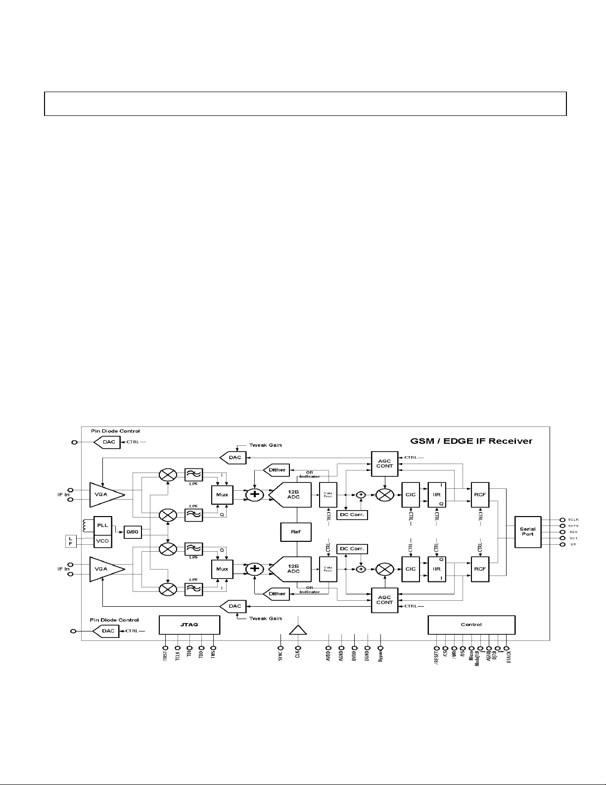
Diversity IF to Baseband
a
GSM/EDGE Narrowband Receiver
Preliminary Technical Data AD6650
FEATURES
Digital VGA
I & Q Demodulators
Active Low Pass Filters
Dual Wideband ADC
Programmable Decimation and Channel Filters
Phase Locked Loop Circuitry
Serial Data Output Ports
IF Frequencies 70-300MHz
10 dB Noise Figure
+24 dBm Input IP2
-13 dBm Input IP3
3.3 Volt I/O and CMOS Core
2
I
C and Microprocessor Interface
JTAG Boundary Scan
APPLICATIONS
GSM/EDGE Single Carrier and Diversity Receivers
Micro and Pico Cell Systems
Wireless Local Loop
Smart Antenna Systems
Software Radios
In Building Wireless Telephony
PRODUCT DESCRIPTION
The AD6650 is a diversity, IF to baseband receiver for
GSM/EDGE. This narrow band receiver consists of an
integrated DVGA, IF-to-baseband I&Q demodulators, lowpass filtering, and a dual wideband ADC. The chip can
accommodate IF input frequencies from 70 MHz to 300 MHz.
This receiver architecture is designed such that only one
external SAW filter(one for main and one for diversity) is
required in the entire Rx signal path to meet GSM/EDGE
blocking requirements.
Digital decimation and filtering circuitry is embedded on chip
to generate serial output I&Q
filters remove unwanted signals and noise outside the channel
of interest. In addition, programmable RAM Coefficient
filters allow anti-aliasing, matched filtering, and static
equalization functions to be combined in a single, costeffective filter.
The AD6650 is part of a complete GSM/EDGE receive and
transmit chipset. Other components in this chipset are: RF to
IF amplifier/mixers, receive and transmit frequency hopping
synthesizers, and a baseband to IF transmit modulator and
ramping chip.
data streams. The decimating
Figure 1. AD6650 Functional Block Diagram
PrJ 02/27/03
Information furnished by Analog Devices is believed to be accurate and
reliable. However, no responsibility is assumed by Analog Devices for its
use, nor for any infringements of patents or other rights of third parties that
may result from its use. No license is granted by implication or otherwise
under any patent or patent rights of Analog Devices. Trademarks and
registered trademarks are the property of their respective companies.
One Technology Way, P.O. Box 9106, Norwood, MA 02062-9106, U.S.A.
Tel: 781/329-4700 www.analog.com
Fax: 781/326-8703 © 2003 Analog Devices, Inc. All rights reserved.
Page 2

Preliminary Technical Data AD6650
TABLE OF CONTENTS
FEATURES . . . . . . . . . . . . . . . . . . . . . . . . . . . . . . . . . . . . xx
PRODUCT DESCRIPTION . . . . . . . . . . . . . . . . . . . . . . . .xx
FUNCTIONAL BLOCK DIAGRAM . . . . . . . . . . . . . . .. .xx
SPECIFICATIONS/CHARACTERISTICS . . . . . .. . . . . . xx
TIMING DIAGRAMS . . . . . . . . . . . . . . . . . . . . . . . . . . . . xx
ABSOLUTE MAXIMUM RATINGS . . . . . . . . . . . . . . . .xx
PIN FUNCTION DESCRIPTIONS . . . . . . . . . . . . . . . . xx
ARCHITECTURE . . . . . . . . . . . . . . . . . . . . . . . . . . . . . . .xx
EXAMPLE FILTER RESPONSE . . . . . . . . . . . . . . . . . . .xx
AGC LOOP.......................................................................xx
DC CORRECTION...........................................................xx
FOURTH ORDER CASCADED INTEGRATOR COMB
FILTER . . . . . . . . . . . . . . . . . . . . . . . . . . . . . . . . . . . . . xx
CIC4 Rejection . . . . . . . . . . . . . . . . . . . . . . . . . . . . . . . xx
INFINITE IMPULSE RESPONSE xx
RAM COEFFICIENT FILTER . . . . . . . . . . . . . . . . . . . . .xx
RCF Decimation Register . . . . . . .. . . . . .. . . . . xx
RCF Decimation Phase . . . . .. . . . . . . . . . . . . . xx
RCF Filter Length . . . . . .. . . . . . . . . . . . . . . . . .xx
RCF Output Scale Factor and Control Register . xx
USER-CONFIGURABLE BUILT-IN SELF-TEST
CHANNEL BIST...........................................xx
CHIP SYNCHRONIZATION . . . . . . . . . . . . . . . . . . . . .xx
Start . . . . . . . . . . . . . . . . .. . . . . . . . . . . . . . . . xx
SERIAL OUTPUT DATA PORT . . . . . . . . . . . . . . . . . . .xx
Serial Output Data Format . . . . . . . . . . . . . . . . . xx
Serial Data Frame (Serial Bus Master) .. . . . . . . . xx
Serial Data Frame (Serial Cascade) . . . . . . . . . xx
Configuring the Serial Ports . . . . . . . .. . . . . . . xx
Serial Port Data Rate . . . . . . . . . .. . . . . . . . . . . . xx
Serial Slave Operation . . . . . . . . . .. . . . . . . . . . . xx
Serial Ports Cascaded . . . . . . . .. . . . . . . . . . . . . . xx
Serial Output Frame Timing (Master and Slave) xx
Serial Port Timing Specifications . . . . . . ... . . . . xx
SCLK . . . . . . . .. . . . . . . . . . . . . . . . . . . . . . . . xx
SDO0 . . . . . . . . . . . . . . . . .. . . . . . . . . . . . . . xx
SDO1 . . . . . . . . . . . . . .. . . . . . . . . . . . . . . . xx
SDFS . . . . . . . . . . . . . .. . . . . . . . . . . . . . . . . . .. . xx
Serial Word Length . . . . . .. . . . . . . . . . . . . . . . . xx
SDFS Mode . . . . . . . . . . . . .. . . . . . . . . . . . . . . . xx
Mapping RCF Data to the BIST Registers . . . .. . xx
0x00: Clock Divider Control . .. . .xx
0x01-0x05: PLL Register[4:0] . . . . . . .. . . . . .. . xx
0x06: Clamp Control............................................xx
MICROPORT CONTROL . . . . . . . . . . . . . . . . . . . . . . . . xx
2
I
JTAG BOUNDARY SCAN . . . . . . . . . . . . . . . . . . . . .xx
INTERNAL WRITE ACCESS . . . . . . . . . . . . . . . .. . . . .xx
Write Pseudocode . . . . . . . . . . . . . . . . . . . . . . . . . . . . . . xx
INTERNAL READ ACCESS . . . . . . . . . . . . . . . . . . . . . . xx
Read Pseudocode . . . . . . . . . . . . . . . . . . . . . . . xx
OUTLINE DIMENSIONS . . . . . . . . . . . . . .. . . . . xx
0x07: Aux DAC A ...............................................xx
0x08: Aux DAC B ................................................xx
0x09: Aux DAC Control.......................................xx
0x0A: ADC Dither Control.................................xx
0x0B: DC Correction BW.....................................xx
0x0C: DC Correction Control...............................xx
0x0D-0x14: AGC Control[7:0]............................xx
0x15: Start Hold-Off Counter...............................xx
0x16: CIC4 Decimation.......................................xx
0x17: CIC4 Scale.................................................xx
0x18: IIR Control Register...................................xx
0x19: RCF Decimation Register..........................xx
0x1A: RCF Decimation Phase..............................xx
0x1B: RCF Coefficient Offset..............................xx
0x1C: RCF Taps....................................................xx
0x1D: RCF Scale Register...................................xx
0x1E-0x1F: BIST For A-I/Q.................................xx
0x20-0x21: BIST for B-I/Q..................................xx
0x22: Serial Control Register...............................xx
0x23-0x29: Reserved............................................xx
0x30-0x5F: Coefficient Memory.........................xx
0x60-0xFF: Reserved...........................................xx
External Memory Map . . . . . .. . . . . . . . . . . . . . . xx
Access Control Register (ACR) . . . . .. . . . . . . . . xx
External Memory Map . . . . . . ... . . . . . . . . . . . . xx
Channel Address Register (CAR) . .. . . . . . . . . . xx
SOFT_SYNC Control Register . .. . . . . . . . . . xx
PIN_SYNC Control Register . . . ... . . . . . . . . . xx
SLEEP Control Register . . . . . . .. . . . . . . . . . . . xx
Data Address Registers . . . . . . .. . . . . . . . . . . . . xx
Write Sequencing . . . . . . . .. . . . . . . . . . . . . . . . . xx
Read Sequencing . . . . . . . .. . . . . . . . . . . . . . . . . xx
Read/Write Chaining . . . . .. . . . . . . . . . . . . . . . . xx
Intel Nonmultiplexed Mode (INM) . . . . . . . . . . . xx
Motorola Nonmultiplexed Mode (MNM) ... . . . . xx
C PORT CONTROL
REV. PrJ 02/27/2003 2
Page 3

Preliminary Technical Data AD6650
AC Specifications
Parameter
Overall Function
Frequency Range 70 300 MHz
Gain Control
Gain Step Size .094 dB
Gain Step Accuracy +/- .5 Step
Baseband Filters
Group Delay 119 124 127 ns
Bandwidth 3.36 3.5 3.64 MHz
LO Phase Noise: @ 200KHz Offset -88 dBc/Hz
@ 400KHz Offset -108 dBc/Hz
@ 600KHz Offset -120 dBc/Hz
@ 800KHz Offset TBD dBc/Hz
@ 1600KHz Offset TBD dBc/Hz
@ 3000KHz Offset TBD dBc/Hz
F = 70 MHz
Min Gain 0 dB
Max Gain 36 dB
Noise Figure1 10.25 dB
Input IP2 +24 dBm
Input IP3 -13 dBm
Image Rejection 35 dBc
FullScale Input Power +4 dBm
Input Impedance 200+jx Ω
F = 150 MHz
Min Gain 0 dB
Max Gain 36 dB
Noise Figure1 10.25 dB
Input IP2 +24 dBm
Input IP3 -13 dBm
Image Rejection 35 dBc
FullScale Input Power +4 dBm
Input Impedance 200+jx Ω
F = 200 MHz
Min Gain 0 dB
Max Gain 36 dB
Noise Figure1 10.25 dB
Input IP2 +24 dBm
Input IP3 -13 dBm
Image Rejection 35 dBc
FullScale Input Power +4 dBm
Input Impedance 200+jx Ω
F = 250 MHz
Min Gain 0 dB
Max Gain 36 dB
Noise Figure1 10.25 dB
Input IP2 +24 dBm
REV. PrJ 02/27/2003 3
Temp
Test
Level
MIN
AD6650BBC
Typ
Max
Units
Page 4

Preliminary Technical Data AD6650
Input IP3 -13 dBm
Image Rejection 35 dBc
FullScale Input Power +4 dBm
Input Impedance 200+jx Ω
F = 300 MHz
Min Gain 0 dB
Max Gain 36 dB
Noise Figure1 10.25 dB
Input IP2 +24 dBm
Input IP3 -13 dBm
Image Rejection 35 dBc
FullScale Input Power +4 dBm
Input Impedance 200+jx Ω
1
This Measurement applies in Maximum Gain (+36 dB)
REV. PrJ 02/27/2003 4
Page 5

Preliminary Technical Data AD6650
DIGITAL SPECIFICATIONS
(TMIN to TMAX, AVDD, CLKVDD, DVDD = +3.3v, unless otherwise noted)
Parameter
VDD IV 3.0 3.3 3.6 V
VDDIO IV 3.0 3.3 3.6 V
AVDD IV 3.0 3.3 3.6 V
T
IV -40 +25 +85
AMBIENT
ELECTRICAL CHARACTERISTICS
Parameter (Conditions)
LOGIC INPUTS
Logic Compatibility Full 3.3V CMOS
Logic “1” Voltage VDD-0.9 VDD V
Logic “0” Voltage 0 0.9 V
Logic “1” Current –10 +10 µA
Logic “0” Current –10 10 µA
Input Capacitance 5 pF
LOGIC OUTPUTS
Logic Compatibility Full 3.3VCMOS/TTL
Logic “1” Voltage (IOH=0.25mA) Full IV 2.4 VDD-0.2 V
Logic “0” Voltage (IOL=0.25mA) Full IV 0.2 0.4 V
IDD SUPPLY CURRENT
CLK=104 MHz (GSM Example)
I
I
I
POWER DISSIPATION
CLK=104 MHz GSM/EDGE Example V 1.2 W
mA
VDD
mA
VDDIO
mA
AVDD
Temp
Temp
+25°C
Test
Level
Test
Level Min
V
MIN
AD6650BBC
Typ
AD6650BBC
Typ
Max
Max
Units
°C
Units
REV. PrJ 02/27/2003 5
Page 6

Preliminary Technical Data AD6650
GENERAL TIMING CHARACTERISTICS
Parameter (Conditions)
CLK Timing Requirements:
t
CLK Period Full I 9.6 ns
CLK
t
CLK Width Low Full IV 0.5 x t
CLKL
t
CLK Width High Full IV 0.5 x t
CLKH
/RESET Timing Requirements:
t
/RESET Width Low Full IV 30 ns
RESL
SYNC Timing Requirements:
tSS
tHS
Master Mode Serial Port Timing Requirements (SBM=1):
Switching Characteristics
t
DSCLK1
t
DSCLKH
t
DSCLKL
t
t
t
t
t
DSCLKLL
DSDFS
DSDO
DSD1
DSDR
Slave Mode Serial Port Timing Requirements (SBM=0):
Switching Characteristics
t
SCLK Period Full IV 16.0 ns
SCLK
t
SCLK low time (when SDIV=1, divide by 1) Full IV 5.0 ns
SCLKL
t
SCLK high time (when SDIV=1, divide by 1) Full IV 5.0 ns
SCLKH
t
DSDO
t
DSD1
t
DSDR
SYNC to ↑CLK Setup Time
SYNC to ↑CLK Hold Time
2
↑CLK to ↑SCLK Delay (divide by 1)
↑CLK to ↑SCLK Delay (for any other divisor)
↑CLK to ↓SCLK Delay (divide by 2 or even #)
↓CLK to ↓SCLK Delay (divide by 3 or odd #)
↑SCLK to SDFS Delay
↑SCLK to SDO Delay
↑SCLK to SD1 Delay
↑SCLK to DR Delay
2
↑SCLK to SDO Delay
↑SCLK to SD1 Delay
↑SCLK to DR Delay
Input Characteristics
t
t
SSF
HSF
SDFS to ↑SCLK Setup Time
SDFS to ↑SCLK Hold Time
1
All Timing Specifications valid over VDD range of 3.0V to 3.6V and VDDIO range of 3.0V to 3.6V.
2
The timing parameters for SCLK, SDFS, SDO0, SDO1, and DR apply to both channels (0, 1). The Slave serial port’s (SCLK)
operating frequency is limited to 52 MHz.
3
Specification pertains to control signals: RW, (/WR), /DS, (/RD), /CS
4
(C
=40pF on all outputs unless otherwise specified)
LOAD
Temp
Test
Level Min
AD6650
Typ
CLK
CLK
Max
Units
ns
ns
Full IV ns
Full IV ns
Full IV
3.9
13.4
ns
Full IV 4.4 14.0 ns
Full IV 3.25 6.7 ns
Full IV 3.8 6.9 ns
Full IV 3.02 ns
Full IV 2.7 ns
Full IV 2.6 ns
Full IV 2.7 ns
Full IV 6.8 ns
Full IV 6.8 ns
Full IV 6.9 ns
Full IV 2.6 ns
Full IV -1.15 ns
REV. PrJ 02/27/2003 6
Page 7

Preliminary Technical Data AD6650
MICROPROCESSOR PORT TIMING CHARACTERISTICS
Test
Temp
Level Min
MICROPROCESSOR PORT, MODE INM (MODE=0)
MODE INM Write Timing:
t
SC
tHC
t
HWR
t
Address/Data to /WR(RW) Setup Time Full IV -0.5 ns
SAM
t
Address/Data to RDY(/DTACK) Hold Time Full IV 7.0 ns
HAM
t
/WR(RW) to RDY(/DTACK) Delay Full IV 4.0 ns
DRDY
t
/WR(RW) to RDY(/DTACK) High Delay Full IV 4*t
ACC
Control
Control
/WR(RW) to RDY(/DTACK) Hold Time
MODE INM Read Timing:
t
SC
tHC
t
SAM
t
Address to Data Hold Time Full IV 7.0 ns
HAM
Control
Control
Address to /RD(/DS) Setup Time
3
to ↑CLK Setup Time
3
to ↑CLK Hold Time
3
to ↑CLK Setup Time
3
to ↑CLK Hold Time
Full
Full
Full
Full
Full
Full
IV
IV
IV
IV
IV
IV
5.5
1.0
8.0
CLK
4.0
2.0
0.0
tZD Data Tri-state Delay Full IV ns
tDD RDY(/DTACK) to Data Delay Full IV ns
t
/RD(/DS) to RDY(/DTACK) Delay Full IV 4.0 ns
DRDY
t
/RD(/DS) to RDY(/DTACK) High Delay Full IV 4*t
ACC
MICROPROCESSOR PORT, MODE MNM (MODE=1)
MODE MNM Write Timing:
t
SC
tHC
t
HDS
t
RW(/WR) to /DTACK(RDY) Hold Time Full IV 8.0 ns
HRW
t
Address/Data To RW(/WR) Setup Time Full IV -0.5 ns
SAM
t
Address/Data to RW(/WR) Hold Time Full IV 7.0 ns
HAM
t
/DS(/RD) to /DTACK(RDY) Delay Full IV ns
DDTACK
t
RW(/WR) to /DTACK(RDY) Low Delay Full IV 4*t
ACC
Control
Control
/DS(/RD) to /DTACK(RDY) Hold Time
MODE MNM Read Timing:
t
SC
tHC
t
HDS
t
Address to /DS(/RD) Setup Time Full IV 0.0 ns
SAM
t
Address to Data Hold Time Full IV 7.0 ns
HAM
Control
Control
/DS(/RD) to /DTACK(RDY) Hold Time
3
to ↑CLK Setup Time
3
to ↑CLK Hold Time
3
to ↑CLK Setup Time
3
to ↑CLK Hold Time
Temp
Full
Full
Full
Full
Full
Full
Test
Level Min
IV
IV
IV
IV
IV
IV
CLK
5.5
1.0
8.0
CLK
4.0
2.0
8.0
tZD Data Tri-State Delay Full IV ns
tDD /DTACK(RDY) to Data Delay Full IV ns
t
/DS(/RD) to /DTACK(RDY) Delay Full IV ns
DDTACK
t
/DS(/RD) to /DTACK(RDY) Low Delay Full IV 4*t
ACC
CLK
MODE I2C Timing:
t
DSCL
t
DSDA
5
t
SSCL
1
All Timing Specifications valid over VDD range of 3.0V to 3.6V and VDDIO range of 3.0V to 3.6V.
2
The timing parameters for SCLK, SDFS, SDO0, SDO1, and DR apply to both channels (0, 1)
3
Specification pertains to control signals: RW, (/WR), /DS, (/RD), /CS
4
(C
=40pF on all outputs unless otherwise specified)
LOAD
5
There is no hold time for SDA because as this waits for a negative transition (↓) on SCL to transition.
↑SCL to SDA Delay
SDA to ↑SCL Delay
↑CLK to ↑SCL Delay
Full IV 61 ns
Full IV 57 ns
Full IV 5 ns
AD6650
5*t
7*t
AD6650
5*t
7*t
1
Typ
Max
ns
CLK
ns
CLK
Max
Typ
ns
CLK
ns
CLK
Units
ns
ns
ns
ns
ns
ns
Units
ns
ns
ns
ns
ns
ns
REV. PrJ 02/27/2003 7
Page 8
Preliminary Technical Data AD6650
TIMING DIAGRAMS
RESET
t
CLK
SCLK
t
DSCLKH
SSF
Figure x. Reset Timing Requirements
t
SCLKH
t
SCLKL
Figure x. SCLK Switching Characteristics (Divide by 1)
CLK
t
DSCLKH
SCLK
Figure x. SCLK Switching Characteristics (Divide by 2 or EVEN integer)
CLK
t
DSCLKH
SCLK
t
DSCLKL
t
DSCLKLL
Figure x. SCLK Switching Characteristics (Divide by 3 or ODD integer)
REV. PrJ 02/27/2003 8
Page 9
Preliminary Technical Data AD6650
TIMING DIAGRAMS
SCLK
t
DSDFS
SDFS
t
SDI
t
SSI
HSI
DATAn
CLK
DR
SCLK
DR
t
DDR
t
DSDR
Figure x. Serial Port Switching Characteristics
Figure x. CLK, DR Switching Characteristics
Figure x. SCLK, DR Switching Characteristics
SCLK
SDFS
t
SSF
t
HSF
Figure x. SDFS Timing Requirements (SBM=0)
REV. PrJ 02/27/2003 9
Page 10

Preliminary Technical Data AD6650
TIMING DIAGRAMS
CLK
t
SS
SYNC
Figure x. SYNC Timing Inputs
TIMING DIAGRAMS – INM Microport Mode
CLK
/RD (/DS)
t
t
SAM
t
SAM
SC
Valid Address
Valid Data
t
DRDY
t
HAM
t
HAM
/WR (RW)
/CS
A[2:0]
D[7:0]
RDY
(/DTACK)
Notes:
Access time depends on the Address accessed. Access time is measured from FE of /WR to RE of RDY .
1. t
ACC
requires a maximum of 9 CLK periods
t
ACC
Figure 16. INM Microport Write Timing Requirements.
t
HS
t
HC
t
HWR
t
ACC
CLK
t
/RD (/DS)
/WR (RW)
/CS
A[2:0]
D[7:0]
RDY
(/DTACK)
Notes:
Access time depends on the Address accessed. Access time is measured from FE of /WR to RE of RDY.
1. t
ACC
requires a maximum of 13 CLK periods and applies to A[2:0]=7,6,5,3,2,1
t
ACC
SC
t
SAM
Valid Addre ss
t
t
ZD
t
DRDY
t
DD
Valid Data
t
ACC
HA
Figure 17. INM Microport Read Timing Requirements.
REV. PrJ 02/27/2003 10
t
HC
t
ZD
Page 11

Preliminary Technical Data AD6650
TIMING DIAGRAMS – MNM Microport Mode
CLK
t
SC
/DS ( /RD)
RW (/WR)
/CS
t
SAM
A[2:0]
D[7:0]
/DTA CK
(RDY)
Notes:
1. t
Access time depends on the Address accessed. Access time is measured from the FE of /DS to the FE of /DTACK.
ACC
t
requires a maximum of 9 CLK periods
ACC
t
SAM
Valid Address
Valid Data
Figure x. MNM Microport Write Timing Requirements.
t
HC
t
HDS
t
HRW
t
HAM
t
HAM
t
DDTACK
t
ACC
CLK
t
t
SC
/DS (/RD)
RW (/WR)
/CS
t
SAM
A[2:0]
t
D[7:0]
/DTACK
(RDY)
Notes:
1. t
Access time depen ds on the Address accessed. Acce ss time is measured from the FE of /DS to the FE of /DTACK.
ACC
requires a maximum of 13 CLK periods
t
ACC
ZD
t
DD
HC
t
HDS
Valid Address
t
HA
Valid Data
t
DDTACK
t
ACC
Figure x. MNM Microport Read Timing Requirements.
t
ZD
REV. PrJ 02/27/2003 11
Page 12

Preliminary Technical Data AD6650
ABSOLUTE MAXIMUM RATINGS1
Supply Voltage…………….…………….....-0.3V to 3.3v
Input Voltage………..……….........................-0.3 to 3.6V
Output Voltage Swing…………..-0.3V to VDDIO +0.3V
Load Capacitance…………………..…………….200pF
Junction Temperature Under Bias…..….……….+125°C
Storage Temperature Range……….......-65°C to +150°C
Lead Temperature (5 sec)…………..……….…..+280°C
Notes
1
Stresses greater than those listed above may cause permanent damage to the device These are stress ratings only; functional operation of the devices at these or any
other conditions greater than those indicated in the operational sections of this specification is not implied. Exposure to absolute maximum rating conditions for
extended periods may affect device reliability.
Thermal Characteristics
121-Pin Ball Grid Array:
=28.1°C /Watt, no airflow
θ
JA
θ
=XX°C/Watt, 200-lfpm airflow
JA
Thermal measurements made in the horizontal position on a 4-layer board
EXPLANATION OF TEST LEVELS
I 100% Production Tested.
II 100% Production Tested at 25°C, and Sampled Tested at Specified Temperatures.
III Sample Tested Only
IV Parameter Guaranteed by Design and Analysis
V Parameter is Typical Value Only
VI 100% Production Tested at 25°C, and Sampled Tested at Temperature Extremes
ORDERING GUIDE
Model
AD6650BBC1
AD6650/PCB Evaluation Board with AD6650 and Software
Notes
1
X-Grade Material is Pre-Production material, normally shipped during product characterization and qualification.
Temperature Range
-40°C to +85°C (Ambient)
ESD SENSITIVITY
The AD6650 is an ESD (electrostatic discharge) sensitive device. Electrostatic charges as high as 4000 V readily accumulate on
the human body and test equipment and can discharge without detection. Although the AD6650 features proprietary ESD
protection circuitry, permanent damage may occur on devices subjected to high-energy electrostatic discharges. Therefore, proper
ESD precautions are recommended to avoid performance degradation or loss of functionality.
.
Package Description
121- Pin Ball Grid Array
Package
Option
REV. PrJ 02/27/2003 12
Page 13

Preliminary Technical Data AD6650
Pin Configuration
1 2 3 4 5 6 7 8 9 10 11
DGND TDI TMS /TRST /RESET DNC AVDD CLK /CLK AGND AGND
A
SDFS SCLK TDO TCLK SYNC DNC AVDD AVDD AGND AGND /BIN
B
SD1 SD0 DVDD DVDD DVDD DVDD AVDD AVDD AGND AGND BIN
C
D7 DR DVDD DGND DGND DGND AVDD AVDD AGND AGND AGND
D
D5 D6 DVDD DGND DGND DGND AVDD AVDD AGND AGND LF
E
D3 D4 DVDD DGND DGND DGND AVDD AVDD AGND XVCOB XVCO
F
D1 D2 DVDD DGND DGND DGND AVDD AVDD AGND AGND CP
G
/DS D0 DVDD DGND DGND DGND AVDD AVDD AGND AGND AGND
H
RW /DTACK DVDD DVDD DVDD DVDD AVDD AVDD AGND AGND AIN
J
A2 A1 /CS MODE1 CHIP_ID1 DNC AVDD REFGND REFT AGND /AIN
K
DGND A0 MODE2 MODE0 CHIP_ID0 DNC AVDD VREF REFB AGND AGND
L
1 2 3 4 5 6 7 8 9 10 11
Pin Function Descriptions
Name Type Function # of Pins
POWER SUPPLY
DVDD P 3.3V Digital Core/IO Supply
AVDD P 3.3V Analog Supply
DGND G Digital Ground
AGND G Analog Ground
INPUTS
/RESET I Active Low Reset Pin
SYNC I Synchronizes Digital Filters and AGC loop
CHIP_ID[1:0] I
SERIAL DATA PORT
SCLK I/O Bi-directional Serial Clock
SDFS I/O Bi-directional Serial Data Frame Sync
SD0 O/T Serial Data Output
SD1 O/T Serial Data Output
DR O Output Data Ready Indicator
1
MICROPORT/SERIAL CONTROL
2
D[7:0] I/O/T Bi-directional Microport Data
A[2:1] I Microport Address Bits 2 and 1
A0 I/O/T Microport Adress bit 0
/CS I Chip Select
/DS(/RD) I/O/T Active Low Data Strobe (Active Low Read)
/DTACK(RDY) I/O/T Active Low Data Acknowledge (Microport Status Bit)
RW(/WR) I/O/T Read Write (Active Low Write)
MODE[2:0] I Selects Control Port Mode
JTAG
/TRST I Test Reset Pin
TCLK I Test Clock Input
TMS I Test Mode Select Input
Chip ID
A
B
C
D
E
F
G
H
J
K
L
13
9
17
22
1
1
2
1
1
1
1
1
8
2
1
1
1
1
1
3
1
1
1
REV. PrJ 02/27/2003 13
Page 14

Preliminary Technical Data AD6650
TDO O/T Test Data Output
TDI I Test Data input
Analog Inputs
Ain I Main Analog Input
Ain/ I Complement of AIN, differential analog input
Bin I Diversity Analog Input
Bin/ I Complement of BIN, differential analog input
PLL Inputs
CPOut O Charge Pump Out
LF I Loop Filter
XVCO I External VCO Input [No Connection required if internal
XVCOB I External VCO Input Complement [No connection required
REFT; REFB; VREF O Internal ADC Voltage Reference; bypass to ground with
REFGND G ADC Ground Reference; See Schematic for Proper hook-up
Clock Inputs
CLK I Encode Input, conversion initiated on rising edge
CLK/ I Complement of Encode
DNC N/A Do Not Connect
VCO used]
if internal VCO used]
capacitor[3]; See Schematic for Proper hook-up
1
1
1
1
1
1
1
1
1
3
1
1
4
REV. PrJ 02/27/2003 14
Page 15

Preliminary Technical Data AD6650
ARCHITECTURE
The AD6650 is a mixed-signal received signal processor
intended for direct IF sampling radios requiring high symbol
rate. It has been optimized for the demanding filtering
requirements of GSM and EDGE.
The AD6650 has five signal processing stages: a digital
VGA, I&Q Demodulators, 7
wideband ADC, and Digital Filtering and Control Stage.
Programming and control is accomplished via serial and
microprocessor interfaces.
DVGA
A gain ranging digital VGA is used to extend the dynamic
range of the input signal and prevent signal clipping at the
ADC input.
I&Q Demodulators
Frequency translation is accomplished with I&Q demodulators.
Real data entering this stage is separated into in-phase (I) and
quadrature (Q) components. This stage translates the input
signal from an intermediate frequency (IF) to a baseband
frequency.
Low Pass Filters
Following frequency translation is a 7
Active Filter with a 3.5 MHz Bandwidth and RC calibration.
Dual ADCs
The ADC is implemented by providing dual track and holds
in front of an AD9238 ADC core. In front of each ADC is a
MUX operating at 52 MSPS.
VCO/PLL
A voltage controlled oscillator and phase locked loop
circuit generates the appropriate IF frequency for the
demodulators.
DIGITAL FILTERS
Following the analog frequency translation is a fourth order
Cascaded Integrator Comb (CIC4) filter whose response is
defined by the decimation rate.
IIR Stage Next
The final stage is a sum-of-products FIR filter with
programmable 20-bit coefficients, and decimation rates
programmable from 1 to 4. The RAM Coefficient FIR filter
(RCF in the Functional Block Diagram) can handle a maximum
of 48 taps.
The overall filter response for the AD6650 is the composite of
all decimating. Each successive filter stage is capable of
REV. PrJ 02/27/2003 15
th
Order Low Pass Filters, dual
th
Order Low Pass
narrower transition bandwidths but requires a greater number of
CLK cycles to calculate the output. More decimation in the first
filter stage will minimize overall power consumption. Data from
the chip is interfaced to the DSP via a high-speed synchronous
serial port.
Theory of Operation
AGC LOOP
The AGC consists of three gain control loops; a slow loop
following the ADC, a Fast Attack (FA) loop following the base
band filter, and the Fast Decay (FD) loop following the
decimation filters.
Slow Loop
The slow loop is the main loop and has a ‘Loop gain’ parameter
1
) associated with it. This parameter controls the rate of
(p4
change of the gain and should always be less than 1. The default
loop gain used is 1/256. The slow loop attempts to maintain the
signal entering the ADC at a given level, which is referred to as
the ‘Requested level’ (p5). This level is specified to the loop in
dBFS. This level can be between 0dBFS and –24dBFS of the
converter in .094dB resolution. The default value is –6.02
dBFS. The slow loop has a ‘peak detect’ function, the period of
which can be set by the user (p1). This ‘peak detect’ period can
be set to 1/4 of a symbol period or greater to prevent the AGC
loop from gaining off the envelope of the EDGE signal. This
works since the Peak Detector works off of the function
dB(max(|I|,|Q|)) which reflects all of the IQ samples back into
one quadrant of the IQ plane. At a 26MHz sampling frequency,
1 symbol period turns out to be 96 clock cycles; therefore, to
obtain a peak detect period of 1/4 symbol, the period should be
set to 24 samples.
Fast Attack Loop
The FA loop is based off of an analog threshold detector that
prevents overdrive of the analog signal path. In a situation that
could potentially overdrive the converter, the FA loop takes over
from the slow loop and decreases the gain to the VGA front end.
The step size used for the FA loop is programmable between 0
and 1.504dB in .094 dB steps(p0). The FA loop also has a
counter, which is programmable between 1 and 16. When
initialized to ‘Count+1’, the FA loop decreases the gain for
‘Count+1’ clock cycles when the threshold is crossed.
Page 16

Preliminary Technical Data AD6650
Fast Decay Loop
The Fast Decay (FD) loop is a fast loop that increases the gain
when the signal falls below a threshold during a deep channel
fade or on the Ramp Down. The fast loop accomplishes this
task by looking at two outputs. The first is the peak signal plus
blocker level at the ADC output (which includes the signal and
any blockers that may be passed through by the SAW filter).
The second is the peak signal level after the decimation filters
and a Blocker Reject Filter have attenuated the blockers. There
are two programmable levels that determine when this loop is
activated: the Signal Plus Blocker level (SPB_level) and the
Signal level (SIG_level). Both these levels are defined in dBFS.
Default values stand at –40dBFS for the SPB_level and –
60dBFS for the SIG_level. When the ‘wideband’ signal is below
the SPB level (p12) and ‘narrowband’ information is below the
Signal level (p13), the FD loop is activated. This loop overrides
the slow loop and has a programmable step size (p7) (currently
set at 0.094dB) and a programmable peak detect period (p6)
currently set at 4 samples at 1.08MHz.
FOURTH ORDER CASCADED INTEGRATOR COMB FILTER
The CIC4 processing stage implements a sharp fixedcoefficient decimating filter, which is driven by the 12 bit
Analog to Digital converter. The maximum input rate into
this filter is ADC
The decimation ratio, MCIC4, may be programmed from 8
to 32 (all integer values). The frequency response of the
filter is given by Equation x. The gain and passband droop
of CIC4 should be calculated by these equations. Both
parameters may be compensated for in the IIR stage.
)(4
zCIC
M
REV. PrJ 02/27/2003 16
, which cannot exceed 26 MHz.
OUTPUT
4
M
4
CIC
−
1
z
CIC
−
−
11
z
⋅=
−
1
4
4
)(4
fCIC
1
M
CIC
sin
⋅=
4
sin
⋅
Mf
⋅
π
f
ADC
f
⋅
π
f
ADC
CIC
4
The scale factor, SCIC4 is a programmable unsigned integer
between 12 and 20. It serves to control the attenuation of the data
into the CIC4 stage in 6 dB increments. For the best dynamic
range, SCIC4 should be set to the smallest value possible (lowest
attenuation) without creating an overflow condition.
()()
ADC
M
25
OUTPUT
CIC
The output rate of this stage is given by equation x.
f ≤
SAMP
CIC4 Rejection
Table xx illustrates the amount of bandwidth in percentage of the
clock rate that can be protected with various decimation rates
and alias rejection specifications. The maximum input rate into
the CIC4 is 26 MHz, as mentioned above. As in Table xx, these
are the ½ bandwidth characteristics of the CIC4.
Table x. SSB CIC4 Alias Rejection Table
12log4
−×= MceilS
44CIC
-50 -60 -70 -80 -90 -100
8 2.602 2.751 2.867 2.957 3.027 3.080
9 2.311 2.444 2.547 2.627 2.690 2.737
10 2.078 2.199 2.291 2.364 2.420 2.463
11 1.889 1.998 2.083 2.148 2.200 2.239
12 1.731 1.831 1.909 1.969 2.016 2.052
13 1.597 1.690 1.761 1.817 1.861 1.894
14 1.483 1.569 1.635 1.687 1.728 1.759
15 1.384 1.464 1.526 1.575 1.613 1.641
16 1.297 1.373 1.431 1.476 1.512 1.539
17 1.221 1.292 1.346 1.389 1.423 1.448
18 1.153 1.220 1.272 1.312 1.344 1.368
19 1.092 1.156 1.205 1.243 1.273 1.296
20 1.037 1.098 1.144 1.181 1.209 1.231
21 0.988 1.045 1.090 1.124 1.152 1.172
22 0.943 0.998 1.040 1.073 1.099 1.119
23 0.902 0.954 0.995 1.027 1.051 1.070
24 2.602 2.751 2.867 2.957 3.027 3.080
25 0.830 0.878 0.915 0.944 0.967 0.985
26 0.798 0.844 0.880 0.908 0.930 0.947
27 0.768 0.813 0.847 0.874 0.896 0.912
28 0.741 0.784 0.817 0.843 0.864 0.879
Page 17

Preliminary Technical Data AD6650
29 0.715 0.757 0.789 0.814 0.834 0.849
30 0.691 0.732 0.763 0.787 0.806 0.820
31 0.669 0.708 0.738 0.762 0.780 0.794
32 0.648 0.686 0.715 0.738 0.756 0.769
This table helps to calculate an upper bound on decimation,
MCIC4, given the desired filter characteristics.
INFINITE IMPULSE RESPONSE FILTER
The IIR filter of the AD6650 is a 7th order low-pass filter
with an Infinite Impulse response. The Z-Transform and
coefficients of this filter are shown below.
n
xx_truncz()
0.046227
0.278961
n
= d
0.76021
1.208472
0
:=
5
z7⋅ n2z
+ n3z3⋅+ n1z⋅+ n1z6⋅+ n3z4⋅+ n2z2⋅+ n0+
d7z7d5z5⋅+ d3z3⋅+ d1z⋅+
0
=
0.012895
0
0.254698
0
1.026276
0
1
2⋅
RAM COEFFICIENT FILTER
The final signal processing stage is a sum-of-products
decimating filter with programmable coefficients, see Figure x.
The data memories I-RAM and Q-RAM store the 24 most
recent complex samples from the previous filter stage with 23bit resolution. The coefficient memory, CMEM, stores up to 48
coefficients with 20-bit resolution. On every CLK cycle, one tap
for I and one tap for Q are calculated using the same coefficients.
The RCF output consists of 16 or 24-bit data bits.
RCF Decimation Register
Each RCF channel can be used to decimate the data rate.
The decimation register is a 2 bit register and can decimate
from 1 to 4. The RCF decimation is stored in 0x18 in the
form of M
RCF Decimation Phase Register
The AD6650 filter channel uses the value stored in this
register to pre-load the RCF counter. Therefore instead of
starting from 0, the counter is loaded with this value, thus
creating an offset in the processing that should be equivalent
REV. PrJ 02/27/2003 17
-1. The input rate to the RCF is f
RCF
SAMPIIR
.
to the required processing delay. This data is stored in 0x19
as a 2-bit number.
RCF Filter Length
The maximum number of taps this filter can calculate, N
is given by the equation below. The value N
to the channel register within the AD6650 at address 0x1B.
N
taps
The RCF coefficients are located in addresses 0x40 to 0x6F
and are interpreted as 20-bit 2’s complement numbers.
When writing the coefficient RAM, the lower addresses will
be multiplied by relatively older data from the IIR and the
higher coefficient addresses will be multiplied by relatively
newer data from the IIR. The coefficients need not be
symmetric and the coefficient length, N
odd. If the coefficients are symmetric, then both sides of the
impulse response must be written into the coefficient RAM.
The RCF stores the data from the IIR
23x24 is assigned to I data and 23x24 is assigned to Q data.
The RCF uses the RAM as a circular buffer, so that it is
difficult to know in which address a particular data element
is stored. To avoid start-up transients due to undefined data
RAM values, the data RAM should be cleared upon
initialization.
When the RCF is triggered to calculate a filter output, it
starts by multiplying the oldest value in the data RAM by the
first coefficient, which is pointed to by the RCF Coefficient
Offset Register (0x1A). This value is accumulated with the
products of newer data words multiplied by the subsequent
locations in the coefficient RAM until the coefficient
address RCF
Coefficient
Address
0 h(0) N(0) oldest
1 h(1) N(1)
2 =(N
taps
The RCF Coefficient Offset register can be used for two
purposes. The main purpose of this register is to allow for
multiple filters to loaded into memory and selected simply
by changing the offset as a pointer for rapid filter changes.
The other use of this register is to form part of symbol
timing adjustment. If the desired filter length is padded with
zeros on the ends, then the starting point can be adjusted to
form slight delays in when the filter is computed with
reference to the high-speed clock. This allows for vernier
adjustment of the symbol timing. Course adjustments can be
made with the RCF Decimation Phase.
+N
OFF
- 1) h(2) N(2) newest
Table xx. Three-tap Filter
≤ 48,min
-1 is reached.
taps
Impulse
Response
Mf
⋅
RCFCLK
f
SAMPIIR
taps
into a 46x24 RAM.
-1 is written
taps
, may be even or
Data
taps
,
Page 18

Preliminary Technical Data AD6650
The output rate of this filter is determined by the output rate
of the IIR stage and M
RCF
.
f =
SAMPR
SAMPIIR
M
RCF
f
RCF Output Scale Factor and Control Register
Register 0x1C is used to configure the scale factor for RCF
filter. This 2 bit register is used to scale the output data in 6
dB increments. The possible output scales range from 0 to –
18 dB.
0
10
20
30
40
50
Rejection, dBc
60
70
80
90
100
13 9.75 6.5 3.25 0 3.25 6.5 9.75 13
0
10
20
30
40
50
60
70
80
90
100
110
120
1.98 1.46 0.94 0.43 0 0.61 1.13 1.65 2.17
Gemini Digital Composite Response
CIC4 Response
IIR Filter Response
CIC4 Response, Mcic4 = 24
Offset from Channel Center, MHz
Composite Digital Response with 8x Rate
.17
Frequency in MHz
REV. PrJ 02/27/2003 18
Page 19

Preliminary Technical Data AD6650
SERIAL OUTPUT DATA PORT
The AD6650 has two configurable serial output ports (SDO0,
SDO1). Both ports must be configured the same and
programmed using the same control register. The ports also
share a common SFDS, SCLK, and DR pin for connection to an
external ASIC or DSP. As such, the outputs may be configured
as either serial master or serial slave, but cannot be programmed
independently.
Serial Output Data Format
The AD6650 utilizes a normal linear binary data format with
serial data frame word lengths of 16- or 24-bit precision. In this
mode, the data is shifted out of the device in Big Endian format
(MSB first).
Serial Data Frame Sync (Serial Bus Master)
The serial data frame is initiated with the Serial Data Frame
Sync (SDFS). As each channel within the AD6650 completes a
filter cycle, data is transferred into the serial data buffer. In the
Serial Bus Master (SBM) mode, the internal serial controller
initiates the SDFS on the next rising edge of the serial clock. In
the AD6650, there are 3 or 4 modes in which the frame sync
may be generated as a Serial Bus Master. In the case where both
A and B input channels are processed through SDO0 only, there
are four modes, and when A and B input channels are output
through SDO0 and SDO1 respectively, there are three modes of
operation (mode 0 and 1 are the same). These modes are
described in section SDFS Modes.
Serial Data Frame (Serial Cascade)
Any of the AD6650 serial outputs may be operated in the serial
cascade mode (serial slave). In this mode, the selected AD6650
channel requires that an external device such as a DSP to issue
the serial clock and SDFS.
To operate successfully in the serial cascade mode, the DSP
must have some indication that the AD6650 channel’s serial
buffer is ready to send data. This is indicated by the assertion of
the DR. This pin should be tied to an interrupt or flag pin of the
DSP. In this manner, the DSP will know when to service the
serial port.
When the DSP begins handling the serial service, the serial port
should be configured such that the SDFS pin is asserted one
clock cycle prior to shifting data. As such, the AD6650 channel
samples the SFDS pin on the rising edge of the serial clock. On
the next rising edge of the serial clock the AD6650 serial port
begins shifting data until the specified number of bits have been
shifted.
Configuring the Serial Ports
Both Serial Output Ports can either function as a Master or
Slave, but they cannot be set independently. A Serial Bus
Master will provide SCLK and SDFS outputs. Serial Ports 0 and
1 will always default to serial slaves when RESET is taken low,
but the Serial Ports can be programmed to become master by
setting the SBM bit in the serial control register high.
Serial Port Data Rate
If the Serial Ports are defined as a master, the SCLK frequency
is defined by Equation x.
clock of the AD6650 channel and SDIV is the Serial Division
word for the channel. The SDIV for Serial Port 0 and 1 can be
programmed via the internal control register 0x22.
Serial Slave Operation
The AD6650 can also be operated as a serial bus slave. In this
configuration, shown in Figure x, the serial clock provided by
the DSP can be asynchronous with the AD6650 clock and input
data In this mode the clock has a maximum frequency of 52
MHz and must be fast enough to read the entire serial frame
prior to the next frame coming available. The AD6650 output is
derived (via the Decimation/Interpolation Rates) from its input
sample rate, so the user can determine the output rate. The output
rate of the AD6650 is given below.
Serial Ports Cascaded
Serial output ports may be cascaded on the AD6650. This
allows data to be shifted out of the master and slave channel in
parallel. To accomplish this, the SDFS signal of the master
channel drives the SDFS input of the slave channel
Using the AD6650 master/slave mode permits a DSP to shift the
data from the master AD6650 serial port, in parallel with a frame
of data (I and Q words) from the AD6650 slave port. As shown
in Figure xx, the Master Port is Serial Port 0. The Slave Port is
Serial Port 0 and 1 from another AD6650. The only limit to the
number of ports that can be cascaded comes from serial
bandwidth and fan-out considerations.
There must be enough Serial Clock cycles available to shift the
necessary data into the DSP, and the SCLK (common to all
channels and DSP) must be closely monitored to ensure that it is
a clean signal.
Serial Output Frame Timing (Master and Slave)
The SDFS signal transitions accordingly depending on whether
the part is in Master (SBM = 1, Figure xx) or Slave (SBM = 0,
Figure xx) mode. The next rising edge of SCLK after this occurs
will drive the first bit of the serial data on the SDO pin. The
falling edge of SCLK or the subsequent rising edge can then be
used by the DSP to sample the data until the required number of
bits is received (determined by the serial output port word
length). If the DSP has the ability to count bits, the DSP will
know when the complete frame is received.
fCLK is the frequency of the master
REV. PrJ 02/27/2003 19
Page 20

Preliminary Technical Data AD6650
Serial Port Timing Specifications
Whether the AD6650 serial channel is operated as a Serial Bus
Master or as a Serial Slave, the serial port timing is identical.
Figures xx to xx indicate the required timing for each of the
specification.
t
SCLK
t
SCLKH
SCLK
t
SCLKL
Figure xx. SCLK Timing Requirements
CLK
t
DSCLKH
SCLK
t
SCLKL
t
SCLKH
Figure xx. SCLK Switching Characteristics (Divide by 1)
t
DSDO
SCLK
SCLK
SDFS
SDO
First data is available the first
SCLK after SDFS goes high
Figure xx. Timing for Serial Output Port (SBM=1)
SCLK
SCLK is an output when SBM is high; SCLK is an input when
SBM is low in serial slave mode. All outputs are switched on
the rising edge of SCLK. The SDFS pin is sampled on the
falling edge of SCLK. This allows the AD6650 to recognize the
SDFS in time to initiate a frame on the very next SCLK rising
edge. The maximum speed of this port is 52 MHz.
SDO
SDO is the Serial Data Output. Serial output data is shifted on
the rising edge of SCLK. On the very next SCLK rising edge
after an SDFS, the MSB of the I data from the channel is shifted.
On every subsequent SCLK edge a new piece of data is shifted
out on the SDO pin until the last bit of data is shifted out. The
last bit of data shifted is the LSB of the Channels Q data. SDO is
three-stated when the serial port is outside its time-slot. This
allows the AD6650 to share the SDIN of a DSP with other
AD6650s or other devices.
rising
t
DSO
SDFS minimum
width
is one SCLK
MSB -
MS
I
I
1
B
SDO
I
15
I
14
I
13
Figure xx. Serial Output Data Switching Characteristics
SCLK
SDFS
t
SSF
t
HSF
Figure xx. SDFS Timing Requirements (SBM=0)
.....
SDFS
SDFS is the Serial Data Frame Sync signal. SDFS is an output
when is high in the master mode. SDFS is an input when SBM is
low in the slave mode. SDFS is sampled on the falling edge of
SCLK. When SBM is sampled low, the AD6650 serial port will
function as a serial slave. In this mode, the port is silent until the
DSP issues a frame sync. When the AD6650 detects an SDFS
on the falling edge of a DSP-generated serial clock, on the next
rising edge of the serial clock, the AD6650 enables the output
driver and shifts the MSB of the I word. Data is shifted until the
LSB of the Q word has been sent.
When SBM is sampled high, the chip functions as a serial bus
master. In this mode, the AD6650 is responsible for generating
serial control data. Four modes of that operation are set via
channel address 0x22 Bits 6–5.
Serial Word Length
Bit 4 of register 0x22 determine the length of the serial word (I
or Q). If this bit is set to ‘0,’ each word is 16 bits (16 bits for I
and 16 bits for Q). If this bit is set to ‘1,’ the serial words are 24
bits wide.
REV. PrJ 02/27/2003 20
Page 21

Preliminary Technical Data AD6650
SDFS Modes
As mentioned in the section above, Serial Data Frame Sync,
there are either 3 or 4 modes of operation depending on how the
output of the AD6650 is configured.
Setting Bit 7 of register 0x22 high indicates that input channel A
data is output on SDO0 and input channel B is output on SDO1.
In this condition there are 3 modes of operation (There are
technically 4 modes, but mode 0 and 1 are the same):
Mode 0 and 1 (0x22 Bits 6–5:00; Bit 7:1): The SDFS is valid for
one complete clock cycle prior to the data shift. This single pulse
is valid for output channel SDO0 and SDO1. On the next clock
cycle, the AD6650 begins shifting out the digitally processed
data stream. Depending on the bit precision of the serial
configuration, either 16, or 24 bits of I data are shifted out,
followed by 16 or 24 bits of Q data.
Mode 2 (0x22 Bits 6–5:10; Bit 7:1): Since both SDO0 and
SDO1 are used, SDFS pulses high one clock cycle prior to I data
and also pulses high one clock cycle prior to Q data for each
corresponding input channel. In this mode, there will be 2 SFDS
pulses per each output channel.
Mode 3 (0x22 Bits 6–5:11; Bit 7:1): The SDFS is high for the
entire time that valid bits are being shifted. On SDO0 this will be
either 16 or 24 bits of I data, followed by 16 or 24 bits of Q data
corresponding to input channel A and for SDO1, SDFS remains
high for 16 or 24 bits of I data, followed by 16 or 24 bits of Q
data corresponding to input channel B. The SDFS bit goes high
one complete clock cycle before the first bit shifted out of the
AD6650.
Setting Bit 7 of register 0x22 low indicates that input channel A
and B data will be output to SDO0 only. In this condition there
are 4 modes of operation:
Mode 0 (0x22 Bits 6–5:00; Bit 7:0): The SDFS is valid for one
complete clock cycle prior to the data shift. There is only a
single pulse for both A and B input channels. On the next clock
cycle, the AD6650 begins shifting out the digitally processed
data stream onto SDO0. Depending on the bit precision of the
serial configuration, either 16, or 24 bits of I data, followed by
16 or 24 bits of Q data are shifted out corresponding to input
channel A and then either 16, or 24 bits of I data, followed by 16
or 24 bits of Q data corresponding to input channel B are shifted
out.
Mode 1 (0x22 Bits 6–5:01; Bit 7:0): The SDFS bit goes high one
clock cycle prior to the actual data associated with analog input
channel A. When the I and Q data stream is complete, a second
SDFS is inserted one clock cycle prior to the shift of the data
associated with analog input channel B.
Mode 2 (0x22 Bits 6–5:10; Bit 7:0): SFDS will go high for one
complete clock cycle prior to I data and a second SDFS is
inserted one clock cycle prior to the shift of the first Q bit, both
corresponding to channel A input data. A third and fourth
SDFS are inserted a clock cycle prior to the shift of I and Q data
respectively, which corresponds to input channel B data. In this
mode there will be a total of 4 SFDS pulses.
Mode 3 (0x22 Bits 6–5:11; Bit 7:0): The SDFS is high for the
entire time that valid bits are being shifted, and goes high one
complete clock cycle before the first bit is shifted out of the
AD6650. On SDO0 there will either 16 or 24 bits of I data,
followed by 16 or 24 bits of Q data, then 16 or 24 bits of I data,
followed by 16 or 24 bits of Q data corresponding to input
channel A and B respectively.
MICROPORT CONTROL
The AD6650 has an 8-bit microprocessor port and 4 serial
input ports. The use of each of these ports is described
separately below. The interaction of the ports is then
described. The Microport interface is a multi-mode interface
that is designed to give flexibility when dealing with the host
processor. There are two modes of bus operation: Intel nonmultiplexed mode (INM), and Motorola non-multiplexed
mode (MNM). The mode is selected based on host
processor and which mode is best suited to that processor.
The micro-port has an 8-bit data bus (D[7:0]), 3-bit address
bus(A[2:0]), 3 control pins lines (/CS, /DS or /RD, RW or
/WR), and one status pin (DTACK or RDY). The
functionality of the control signals and status line changes
slightly depending upon the mode that is chosen. Refer to
the timing diagrams and the following descriptions for
details on the operation of both modes.
External Memory Map
The External Memory Map is used to gain access to the
Channel Address Space. The 8-bit data and address buses
are used to set the 8 registers that can be seen in the
following table. These registers are collectively referred to
as the External Interface Registers since they control all
accesses to the Channel Address space as well as global chip
functions. The use of each of these individual registers is
described below in detail.
REV. PrJ 02/27/2003 21
Page 22

Preliminary Technical Data AD6650
External Memory Map
A[2:0] Name Comment
111 Access Control Register
(ACR)
110 Channel Address Register
(CAR)
101 Special Function Register 2
(SF2)
100 Special Function Register 1
(SF1)
011 Special Function Register 0
(SF0)
010 Data Register 2 (DR2) 7-4: Reserved
001 Data Register 1 (DR1) 15-8: D[15:8]
000 Data Register 0 (DR0) 7-0: D[7:0]
7: Auto Increment
6: Broadcast
5-2: Instruction[3:0]
1-0: A[9:8]
7-0: A[7:0]
6: AGC sync Enable
5: DC correction sync enable
4: PN sync enable
3-1: Reserved
0: Issue soft sync
5: First Sync only
4: Enable edge-sensitivity
3-1: Reserved
7-4: Reserved
3: Status of Channel B
2: Enable Channel B
1: Status of Channel A
0: Enable Channel A
3-0: D[19:16]
Table xx. External Memory Map
Access Control Register (ACR)
The Access Control Register serves to define the channel or
channels that receive an access from the micro-port or I
2
C
port.
Bit 7 of this register is the Auto-Increment bit. If this bit is a
1 then the CAR register described below will increment its
value after every access to the channel. This allows blocks
of address space such as Coefficient Memory to be
initialized more efficiently.
Bit 6 of the register is the Broadcast bit and determines how bits
5-2 are interpreted. The Broadcast bit should be set high so that
bits 5-2, which are referred to as Instruction bits (Instruction
[3:0]), allows a single or multiple (up to 4) AD6650 chip(s) to be
configured simultaneously There are 10 possible instructions
that are defined in the table below. The x’s in the table represent
don’t cares in the digital decoding.
REV. PrJ 02/27/2003 22
Microport Instructions
Instruction Comment:
0000 All Chips will get the access.
0001 All Chips will get the access.
0010 All Chips will get the access.
0100 All Chips will get the access.
1000 All Chips with Chip_ID[0] =xxx 0 will get the
1001 All Chips with Chip_ID[0] = xxx1 will get the
1100 All Chips with Chip_ID[1:0] = xx00 will get the
1101 All Chips with Chip_ID[1:0] = xx01 will get the
1110 All Chips with Chip_ID[1:0] = xx10 will get the
1111 All Chips with Chip_ID[1:0] = xx11 will get the
1
A[9:8] bits control which channel is decoded for the access.
access.
access.
access.
access.
access.
access.
1
1
1
1
1
1
Table xx. Microport Instructions
When broadcast is enabled (bit 6 set high) read back is not
valid because of the potential for internal bus contention.
Therefore, if read back is subsequently desired, the
broadcast bit should be set low.
Bits 1-0 of this register are address bits that decode which of
the two channels are being accessed. Because the channels
of the AD6650 cannot be programmed independently, these
bits should be set to 0.
Channel Address Register (CAR)
This register represents the 8-bit internal address of each
channel. If the Auto-Increment bit of the ACR is 1 then this
value will be incremented after every access to the DR0
register, which will in turn access the location pointed to by
this address. The Channel Address register cannot be read
back while the Broadcast bit is set high.
Special Function Registers
The AD6650 has three special function registers, SF0, SF1,
and SF2 that control synchronizing and enabling the
channels. SF0 is the channel enable register, SF1 is the pinsync register, and SF2 is the soft-sync register. For SF0, bits
0 and 2 allow the channels A and B, respectively to come
out of sleep based on the method selected in SF1.Bits 1 and
3 are read-only and indicate whether or not channels A and
B, respectively are active. A 1 indicates the channel is active
and a 0 indicates it is not active. Bits 4 through 7 are
unused.
For SF1, if bit 0 is set to 1,then both channels will wait for a
pulse to appear on the SYNC pin before coming out of sleep;
otherwise, the channels will assume a soft start is desired
and wait for the start hold-off counter to issue a sync. When
bit 5 is set, both channels ignore all subsequent attempts to
resync once they are awake.
For SF2, bit 0 tells the startup block to run the start hold-off
counter from the value programmed into the start hold-off
counter control register and issue a sync when done. Bits 4-
Page 23

Preliminary Technical Data AD6650
6 can be used to enable syncs to individual blocks in the
channels.
Data Address Registers
External Address [2-0] form the data registers DR2, DR1
and DR0 respectively. All internal data words have widths
that are less than or equal to 20 bits. Accesses to External
Address [0] DR0 trigger an internal access to the AD6650
based on the address indicated in the ACR and CAR. Thus
during writes to the internal registers, External Address [0]
DR0 must be written last. At this point data is transferred to
the internal memory indicated in A[9:0]. Reads are
performed in the opposite direction. Once the address is set,
External Address [0] DR0must be the first data register read
to initiate an internal access. DR2 is only 4 bits wide. Data
written to the upper 4 bits of this register will be ignored.
Likewise reading from this register will produce only 4
LSBs.
Write Sequencing
Writing to an internal location is achieved by first writing
the upper two bits of the address to bits 1 through 0 of the
ACR. Bits 7:2 may be set to select the channel as indicated
above. The CAR is then written with the lower eight bits of
the internal address (it doesn’t matter if the CAR is written
before the ACR as long as both are written before the
internal access). Data register 2, (DR2) and register 1 (DR1)
must be written first because the write to data register DR0
triggers the internal access. Data register DR0 must always
be the last register written to initiate the internal write.
Read Sequencing
Reading from the micro port is accomplished in the same
manner. The internal address is set up the same way as the
write. A read from data register DR0 activates the internal
read, thus register DR0 must always be read first to initiate
an internal read followed by DR1and DR2. This provides
the 8 LSBs of the internal read through the micro port
(D[7:0]). Additional data registers can be read to read the
balance of the internal memory.
Read/Write Chaining
The micro port of the AD6650 allows for multiple accesses
while /CS is held low (/CS can be tied permanently low if
the micro port is not shared with additional devices). The
user can access multiple locations by pulsing the /WR or
/RD line and changing the contents of the external three bit
address bus. External access to the external registers of
Table 2 is accomplished in one of two modes using the /CS,
/RD, /WR, and MODE inputs. The access modes are Intel
Non-Multiplexed mode and Motorola Non-Multiplexed
mode. These modes are controlled by the MODE input
(MODE=0 for INM, MODE=1 for MNM). /CS, /RD, and
/WR control the access type for each mode.
REV. PrJ 02/27/2003 23
Programming Modes
The AD6650 can be programmed using several different
modes. These modes include two micro-port modes, Intel
Non-Multiplexed mode and Motorola Non-Multiplexed
Mode, and a serial port mode, I
can be selected by writing the appropriate 3-bit word to the
mode pins. The following table identifies which word
selects the desired mode.
Mode [2:0] Comment:
000 Micro-Port Intel Non-Multiplexed
Mode
001 Micro-Port Motorola Non-Multiplexed
Mode
010 Reserved
011 Reserved
100 I2C
101 Reserved
110 Reserved
111 Reserved
Intel Non-Multiplexed Mode (INM)
Setting the mode word bits to 000 will enable the AD6650
microprocessor in INM mode. The access type is controlled
by the user with the /CS, /RD (/DS), and /WR (RW) inputs.
The RDY (/DTACK) signal is produced by the micro port to
communicate to the user that an access has been completed.
RDY (/DTACK) goes low at the start of the access and is
released when the internal cycle is complete. See the timing
diagrams for both the read and write modes in the
Specifications.
Motorola Non-Multiplexed Mode (MNM)
Setting the mode word bits to 001 will enable the AD6650
microprocessor in MNM mode. The access type is
controlled by the user with the /CS, /DS (/RD), and RW
(/WR) inputs. The /DTACK (RDY) signal is produced by
the micro port to communicate to the user that an access has
been completed. /DTACK (RDY) goes low when an
internal access is complete and then will return high after
/DS (/RD) is de-asserted. See the timing diagrams for both
the read and write modes in the Specifications.
I2C Control
I2C programming is selected by setting MODE =100. I2C is
a two-line bi-directional serial interface specification
developed by Phillips that the AD6650 uses to program the
control registers/ coefficient memory address space. It uses
one data line (SDA) and one clock line (SCL) to transfer
data between a master device and a slave device. The
AD6650 can only act as an I
always needed to program it in I
or the AD6650 comply with the Standard-mode transfer, up
to 100 kHz. An I
slave relying on the wired-and function of the devices
connected to it to indicate that the bus is free. To comply
with this, the I
2
C bus can be multi-master and/or multi-
2
C pins on the AD6650 are open-drain
2
C. The programming mode
2
C slave, so a master device is
2
C mode. I2C data transfers
Page 24

Preliminary Technical Data AD6650
outputs, meaning that they can drive a logic low, but not a
logic high. The pins tri-state to indicate a logic-high and this
is pulled high on the bus by external pull-up resistors to
provide a logic high to the other devices on the bus. For a
single-master, single-slave configuration, a 2.2 k-ohm
resistor should be sufficient on each of the I
2
C lines.
Stable data is transferred on SDA when SCL is high,
meaning that SDA can only be changed when SCL is low. If
SDA transitions while SCL is high, this indicates to the
AD6650 that a new transfer is being initiated on the I
A start condition from the master initiates a transfer between
2
I
C devices and a stop condition ends one. A START
2
C bus.
condition is signaled by transitioning the SDA line from
high to low while SCL is high and a transition from low to
high while SCL is high indicates a STOP condition.
Acknowledge (ACK) is obligatory in I
2
C, so the receiver
must send an acknowledge back to the transmitter after each
byte is transferred. The master generates the acknowledgerelated clock pulse after a given byte is transmitted and
releases the SDA line. The receiver must pull the SDA line
to a stable low before the high period of the extra clock
pulse to signal receipt of the transmitted byte.
2
I
C Access
Once a start condition has been generated, the master must
transmit the AD6650 ’s 1-byte device ID and a read/write bit
to indicate that the rest of the access to follow is intended for
it (the read/write bit and the LSB of the ID are xor ’ed
together to create one byte). The I
2
C device ID of the
AD6650 is 0010 0000 or 20 (hex). Next, the master must
transmit the instruction byte to the AD6650 indicating the
type of access to the EIR.
Bit Comment:
7 Read/Write
6 x
5 SI[2]
4 SI[1]
3 SI[0]
2 A[2]
1 A[1]
0 A[0]
Table xx. I2C Instruction Byte
Each instruction byte indicates whether the EIR is being
written or read (R/Wn), which serial instruction (SI [2:0 ]) is
being executed and which register (A [2:0 ]), if appropriate,
is being accessed. The serial instruction is decoded
according to the following table.
Read/Write SI[2:0] Function
0 000 Write 1 byte: A[2:0] determines
EIR address
0 001 Write 2 bytes: ACR and CAR
0 010 Write 2 bytes: CAR and DR0
0 011 Write 3 bytes: ACR, CAR and
DR0
0 100 Write 4 bytes: ACR, CAR, DR1
and DR0
0 101 Write 5 bytes: ACR, CAR,
DR2, DR1, and DR0
0 110 Write 8 bytes: All EIR
addresses, ACR to DR0
0 111 Write 3 bytes: DR2, DR1, and
DR0
1 000 Read 1 byte: A[2:0] determines
EIR address
1 001 Write 2 bytes: ACR and CAR
1 010 Write 1 byte: CAR; then read 1
byte: DR0
1 011 Write 2 bytes: ACR then CAR;
then read 1 byte: DR0
1 100 Write 2 bytes: ACR then CAR;
then read 2 bytes: DR0 then
DR1
1 101 Write 2 bytes: ACR then CAR;
then read 3 bytes: DR0, DR1,
then DR2
1 110 Read 8 bytes: all EIR addresses
DR0 to ACR
1 111 Read 3 bytes: DR0, DR1, then
DR2
Table xx. I2C Instructions
After the instruction byte, the appropriate data must be
written to or read from the EIR. Finally, a STOP condition is
sent to end the transfer.
Pin Multiplexing
Since the programming modes of the AD6650 are all
mutually exclusive, the pins used for each mode are all
multiplexed together and are named after their microport
function. For I
2
Cmode, the SCL pin is the DSn pin in
microport mode and the SDA pin is the DTACKn pin in
microport mode.
REV. PrJ 02/27/2003 24
Page 25

Preliminary Technical Data AD6650
AD6650 Memory Map
CH Address Register Bit Width Bit Definitions
0 (Hex) Clock Divider Control 0: Clock_DIV
1: Divide by 2
0: No Divide
1 PLL Register 0 22
2 PLL Register 1 22
3 PLL Register 2 22
4 PLL Register 3 22
5 Clamp Control 1: Disable B
0: Disable A
6 Aux DAC A 8 Aux_DACA
7 Aux DAC B 8 Aux_DACB
8 Aux DAC Control 8 7-5: FS Current Adjust B
4: Enable DAC B
3-1: FS Current Adjust A
0: Enable DAC A
9 ADC Dither Control 2 1: High Dither Power
0: Enable Dither
A DC Correction BW 16 15-0: Correction BW
B DC Correction Control 7 6: Multiply by .75
5-2: Scalar
1: PN_EN
0: Enable
C AGC Control 0 4 3: Force VGA Gain
2: FD_Enable
1: FA_Enable
0: Slow Loop Enable
D AGC Control 1 9 8-0: VGA_Gain
E AGC Control 2 16 15-8 Hysterisis
7-0: Requested Level
F AGC Control 3 11 10-8: Loop Gain-Exp
7-0: Loop Gain-Mant
10 AGC Control 4 12 12-10: FD_Step-1
9-8: FA_Thresh
7-4: FA_count
3-0: FA_Step-1
11 AGC Control 5 16 15-8: SpB Peak Detect Period
7-0: S Peak Detect Period
12 AGC Control 6 12 11-0: FD_S Threshold
13 AGC Control 7 12 11-0: FD_SpB Threshold
14 Start Hold-Off Counter 16 Start Hold-Off Counter
15 CIC4 Decimation 5 M
16 CIC4 Scale 4 CIC4_scale
17 IIR Control Register 1 SYNC_MASK
18 RCF Decimation
3 M
Register
19 RCF Decimation Phase 3 P
1A RCF Coefficient Offset 6 CO
1B RCF Taps 6 N
1C RCF Scale Register 2 1-0: Scale
1D BIST for A-I 24 BIST-I/DATA_I
1E BIST for A-Q 24 BIST-Q/DATA_Q
1F BIST for B-I 24 BIST-I/DATA_I
CIC4
RCF
RCF
Taps
RCF
-1
-1
-1
REV. PrJ 02/27/2003 25
Page 26

Preliminary Technical Data AD6650
20 BIST for B-Q 24 BIST-Q/DATA_Q
21 Serial Control Register 9 8: RCF Data to BIST
7: Use SDO1 for B data
6-5: I_SDFS Control
11: High for SDO0 valid
10: AI,AQ,BI,BQ pulses
01: AI,BI pulses
00: AI pulse
4: SOWL
1: 24-bit words
0: 16-bit words
3: SBM
2-0: SDIV[2:0]
23-3F Reserved
40-6F Coefficient Memory 48x20 bit RAM
70-FF Reserved
REV. PrJ 02/27/2003 26
Page 27

Preliminary Technical Data AD6650
Recommended Applications circuit
REV. PrJ 02/27/2003 27
Page 28

Preliminary Technical Data AD6650
Outline Dimensions
Dimensions shown in mm
121-Pin PBGA
REV. PrJ 02/27/2003 28
 Loading...