

Page 1
250 MHz Bandwidth
–
FEATURES
SNR = 65.8 dBFS at fIN up to 250 MHz at 500 MSPS
ENOB of 10.5 bits at f
SFDR = 80 dBc at f
Excellent linearity
DNL = ±0.5 LSB typical, INL = ±0.6 LSB typical
Integrated 16k × 12 FIFO
FIFO readback options
12-bit parallel CMOS at 62.5 MHz
6-bit DDR LVDS interface
SPORT at 62.5 MHz
SPI at 25 MHz
High speed synchronization capability
1 GHz full power analog bandwidth
Integrated input buffer
On-chip reference, no external decoupling required
Low power dissipation
695 mW at 500 MSPS
Programmable input voltage range
1.18 V to 1.6 V, 1.5 V nominal
1.9 V analog and digital supply operation
1.9 V or 3.3 V SPI and SPORT operation
Clock duty cycle stabilizer
Integrated data clock output with programmable clock and
data alignment
up to 250 MHz at 500 MSPS (−1.0 dBFS)
IN
up to 250 MHz at 500 MSPS (−1.0 dBFS)
IN
DPD Observation Receiver
AD6641
GENERAL DESCRIPTION
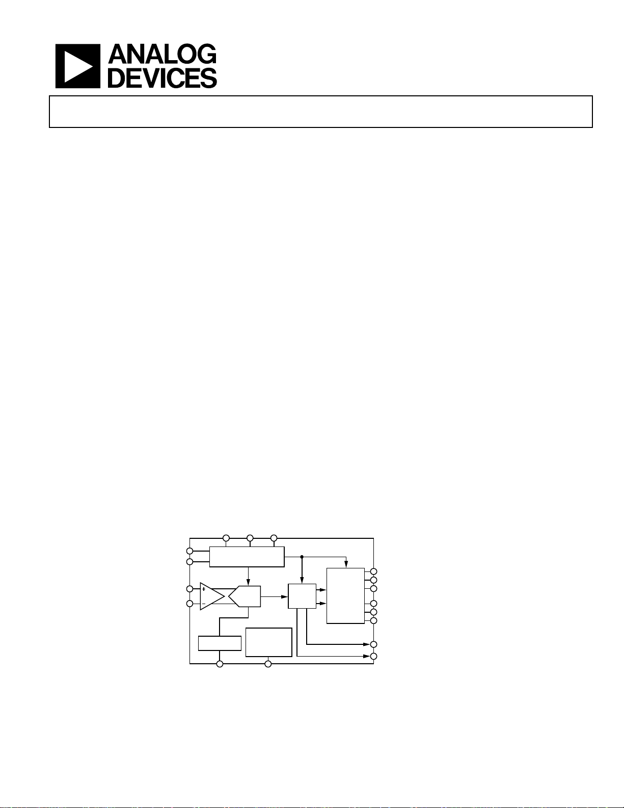
The AD6641 is a 250 MHz bandwidth digital predistortion
(DPD) observation receiver that integrates a 12-bit 500 MSPS
ADC, a 16k × 12 FIFO, and a multimode back end that allows
users to retrieve the data through a serial port (SPORT), the SPI
interface, a 12-bit parallel CMOS port, or a 6-bit DDR LVDS
port after being stored in the integrated FIFO memory. It is optimized for outstanding dynamic performance and low power
consumption and is suitable for use in telecommunications
applications such as a digital predistortion observation path
where wider bandwidths are desired. All necessary functions,
including the sample-and-hold and voltage reference, are
included on the chip to provide a complete signal conversion
solution.
The on-chip FIFO allows small snapshots of time to be captured
via the ADC and read back at a lower rate. This reduces the
constraints of signal processing by transferring the captured
data at an arbitrary time and at a much lower sample rate. The
FIFO can be operated in several user-programmable modes. In
the single capture mode, the ADC data is captured when signaled via the SPI port or the use of the external FILL± pins. In
the continuous capture mode, the data is loaded continuously
into the FIFO and the FILL± pins are used to stop this operation.
APPLICATIONS
Wireless and wired broadband communications
Communications test equipment
Power amplifier linearization
FUNCTIONAL BLOCK DIAGRAM
DUMPFILL+ FILL
CLK+
CLK–
VIN+
VIN–
Rev. 0
Information furnished by Analog Devices is believed to be accurate and reliable. However, no
responsibility is assumed by Anal og Devices for its use, nor for any infringements of patents or ot her
rights of third parties that may result from its use. Specifications subject to change without notice. No
license is granted by implication or otherwise under any patent or patent rights of Analog Devices.
Trademarks and registered trademarks are the property of their respective owners.
CLOCK AND CONTROL
ADC
REFERENCE
VREF
SPI CONTROL
SCLK, SDIO, AND CSB
AND DATA
FIFO
16k × 12
PCLK+
PARALLEL
AND
SPORT
OUTPUTS
Figure 1.
One Technology Way, P.O. Box 9106, Norwood, MA 02062-9106, U.S.A.
Tel: 781.329.4700 www.analog.com
Fax: 781.461.3113 ©2011 Analog Devices, Inc. All rights reserved.
PCLK–
PD[5:0]± IN DDR LVDS MODE
OR PD[11:0] IN CMOS MODE
SP_SCLK
SP_SDFS
SP_SDO
FULL
EMPTY
09813-001
Page 2

AD6641
TABLE OF CONTENTS
Features.............................................................................................. 1
Applications....................................................................................... 1
General Description ......................................................................... 1
Functional Block Diagram .............................................................. 1
Revision History ............................................................................... 2
Product Highlights ........................................................................... 3
Specifications..................................................................................... 4
DC Specifications ......................................................................... 4
AC Specifications.......................................................................... 5
Digital Specifications ................................................................... 6
Switching Specifications.............................................................. 7
SPI Timing Requirements ........................................................... 8
Absolute Maximum Ratings.......................................................... 10
REVISION HISTORY
4/11—Revision 0: Initial Version
Thermal Resistance.................................................................... 10
ESD Caution................................................................................ 10
Pin Configurations and Function Descriptions......................... 11
Typical Performance Characteristics........................................... 15
Equivalent Circuits......................................................................... 18
SPI Register Map ............................................................................ 20
Theory of Operation ...................................................................... 23
FIFO Operation.......................................................................... 23
FIFO Output Interfaces ............................................................. 26
Configuration Using the SPI..................................................... 27
Outline Dimensions....................................................................... 28
Ordering Guide .......................................................................... 28
Rev. 0 | Page 2 of 28
Page 3

AD6641
The data stored in the FIFO can be read back based on several
user-selectable output modes. The DUMP pin can be asserted
to output the FIFO data. The data stored in the FIFO can be
accessed via a SPORT, SPI, 12-bit parallel CMOS port, or 6-bit
DDR LVDS interface. The maximum output throughput
supported by the AD6641 is in the 12-bit CMOS or 6-bit DDR
LVDS mode and is internally limited to 1/8
input sample rate. This corresponds to the maximum output
data rate of 62.5 MHz at an input clock rate of 500 MSPS.
The ADC requires a 1.9 V analog voltage supply and a differential clock for full performance operation. Output format options
include twos complement, offset binary format, or Gray code. A
data clock output is available for proper output data timing. Fabricated on an advanced SiGe BiCMOS process, the device is
available in a 56-lead LFCSP and is specified over the industrial
temperature range (−40°C to +85°C). This product is protected
by a U.S. patent.
th
of the maximum
PRODUCT HIGHLIGHTS
1. High Performance ADC Core.
Maintains 65.8 dBFS SNR at 500 MSPS with a 250 MHz input.
2. Low Power.
Consumes only 695 mW at 500 MSPS.
3. Ease of Use.
On-chip 16k FIFO allows the user to target the high performance ADC to the time period of interest and reduce the
constraints of processing the data by transferring it at an
arbitrary time and a lower sample rate. The on-chip reference and sample-and-hold provide flexibility in system
design. Use of a single 1.9 V supply simplifies system power
supply design.
4. Serial Port Control.
Standard serial port interface supports configuration of the
device and customization for the user’s needs.
5. 1.9 V or 3.3 V SPI and Serial Data Port Operation.
Rev. 0 | Page 3 of 28
Page 4

AD6641
SPECIFICATIONS
DC SPECIFICATIONS
AVDD = 1.9 V, DRVDD = 1.9 V, T
Table 1.
AD6641-500
Parameter1 Temp Min Typ Max Unit
RESOLUTION 12 Bits
ACCURACY
No Missing Codes Full Guaranteed
Offset Error Full −2.6 0.0 +1.8 mV
Gain Error Full −6.8 −2.3 +3.3 % FS
Differential Nonlinearity (DNL) Full ±0.5 LSB
Integral Nonlinearity (INL) Full ±0.6 LSB
TEMPERATURE DRIFT
Offset Error Full 18 μV/°C
Gain Error Full 0.07 %/°C
ANALOG INPUTS (VIN±)
Differential Input Voltage Range2 Full 1.18 1.5 1.6 V p-p
Input Common-Mode Voltage Full 1.8 V
Input Resistance (Differential) Full 1 kΩ
Input Capacitance (Differential) 25°C 1.3 pF
POWER SUPPLY
AVDD Full 1.8 1.9 2.0 V
DRVDD Full 1.8 1.9 2.0 V
SPI_VDDIO Full 1.8 1.9 3.3 V
Supply Currents
3
I
Full 300 330 mA
AVDD
3
I
Full 66 80 mA
DRVDD
Power Dissipation3 Full 695 779 mW
Power-Down Dissipation Full 15 mW
Standby Dissipation Full 72 mW
Standby to Power-Up Time Full 10 μs
1
See the AN-835 Application Note, Understanding High Speed ADC Testing and Evaluation, for a complete set of definitions and information about how these tests were
completed.
2
The input range is programmable through the SPI, and the range specified reflects the nominal values of each setting. See the SPI Register Map section for additional
details.
3
I
AVDD
and I
are measured with a −1 dBFS, 30 MHz sine input at a rated sample rate.
DRVDD
= −40°C, T
MIN
= +85°C, fIN = −1.0 dBFS, full scale = 1.5 V, unless otherwise noted.
MAX
Rev. 0 | Page 4 of 28
Page 5
AD6641
AC SPECIFICATIONS
AVDD = 1.9 V, DRVDD = 1.9 V, T
Table 2.
AD6641-500
Parameter
1, 2
Temp Min Typ Max Unit
SNR
fIN = 30 MHz 25°C 66.0 dBFS
fIN = 125 MHz 25°C 65.9 dBFS
Full 65.0 dBFS
fIN = 250 MHz 25°C 65.8 dBFS
fIN = 450 MHz 25°C 65.1 dBFS
SINAD
fIN = 30 MHz 25°C 66.0 dBFS
fIN = 125 MHz 25°C 65.7 dBFS
Full 63.8 dBFS
fIN = 250 MHz 25°C 65.3 dBFS
fIN = 450 MHz 25°C 64.6 dBFS
EFFECTIVE NUMBER OF BITS (ENOB)
fIN = 30 MHz 25°C 10.7 Bits
fIN = 125 MHz 25°C 10.6 Bits
fIN = 250 MHz 25°C 10.5 Bits
fIN = 450 MHz 25°C 10.4 Bits
SFDR
fIN = 30 MHz 25°C 88 dBc
fIN = 125 MHz 25°C 83 dBc
Full 77 dBc
fIN = 250 MHz 25°C 80 dBc
fIN = 450 MHz 25°C 72 dBc
WORST HARMONIC (SECOND OR THIRD)
fIN = 30 MHz 25°C −92 dBc
fIN = 125 MHz 25°C −77 dBc
Full −84 dBc
fIN = 250 MHz 25°C −80 dBc
fIN = 450 MHz 25°C −72 dBc
WORST OTHER HARMONIC (SFDR EXCLUDING SECOND AND THIRD)
fIN = 30 MHz 25°C −90 dBc
fIN = 125 MHz 25°C −90 dBc
Full −77 dBc
fIN = 250 MHz 25°C −85 dBc
fIN = 450 MHz 25°C −78 dBc
TWO-TONE IMD
f
= 119.8 MHz, f
IN1
= 125.8 MHz (−7 dBFS, Each Tone) 25°C −82 dBc
IN2
ANALOG INPUT BANDWIDTH 25°C 1 GHz
1
All ac specifications tested by driving CLK+ and CLK− differentially.
2
See the AN-835 Application Note, Understanding High Speed ADC Testing and Evaluation, for a complete set of definitions and information about how these tests were
completed.
= −40°C, T
MIN
= +85°C, fIN = −1.0 dBFS, full scale = 1.5 V, unless otherwise noted.
MAX
Rev. 0 | Page 5 of 28
Page 6

AD6641
DIGITAL SPECIFICATIONS
AVDD = 1.9 V, DRVDD = 1.9 V, T
Table 3.
AD6641-500
Parameter1 Temp Min Typ Max Unit
CLOCK INPUTS (CLK±)
Logic Compliance Full CMOS/LVDS/LVPECL
Internal Common-Mode Bias Full 0.9 V
Differential Input Voltage
High Level Input (VIH) Full 0.2 1.8 V p-p
Low Level Input (VIL) Full −1.8 −0.2 V p-p
High Level Input Current (IIH) Full −10 +10 μA
Low Level Input Current (IIL) Full −10 +10 μA
Input Resistance (Differential) Full 8 10 12 kΩ
Input Capacitance Full 4 pF
LOGIC INPUTS (SPI, SPORT)
Logic Compliance Full CMOS
Logic 1 Voltage Full 0.8 × SPI_VDDIO V
Logic 0 Voltage Full 0.2 × SPI_VDDIO V
Logic 1 Input Current (SDIO) Full 0 μA
Logic 0 Input Current (SDIO) Full −60 μA
Logic 1 Input Current (SCLK) Full 50 μA
Logic 0 Input Current (SCLK) Full 0 μA
Input Capacitance 25°C 4 pF
LOGIC INPUTS (DUMP, CSB)
Logic Compliance Full CMOS
Logic 1 Voltage Full 0.8 × DRVDD V
Logic 0 Voltage Full 0.2 × DRVDD V
Logic 1 Input Current Full 0 μA
Logic 0 Input Current Full −60 μA
Input Capacitance 25°C 4 pF
LOGIC INPUTS (FILL±)
Logic Compliance Full CMOS/LVDS/LVPECL
Internal Common-Mode Bias Full 0.9 V
Differential Input Voltage
High Level Input (VIH) Full 0.2 1.8 V p-p
Low Level Input (VIL) Full −1.8 −0.2 V p-p
High Level Input Current (IIH) Full −10 +10 μA
Low Level Input Current (IIL) Full −10 +10 μA
Input Resistance (Differential) Full 8 10 12 kΩ
Input Capacitance Full 4 pF
LOGIC OUTPUTS2 (FULL, EMPTY)
Logic Compliance Full CMOS
High Level Output Voltage Full DRVDD − 0.05 V
Low Level Output Voltage Full DRGND + 0.05 V
LOGIC OUTPUTS2 (SPI, SPORT)
Logic Compliance Full CMOS
High Level Output Voltage Full SPI_VDDIO − 0.05 V
Low Level Output Voltage Full DRGND + 0.05 V
= −40°C, T
MIN
= +85°C, fIN = −1.0 dBFS, full scale = 1.5 V, unless otherwise noted.
MAX
Rev. 0 | Page 6 of 28
Page 7
AD6641
AD6641-500
Parameter1 Temp Min Typ Max Unit
LOGIC OUTPUTS
DDR LVDS Mode (PCLK±, PD[5:0]±, PDOR±)
Logic Compliance Full LVDS
VOD Differential Output Voltage Full 247 454 mV
VOS Output Offset Voltage Full 1.125 1.375 V
Parallel CMOS Mode (PCLK±, PD[11:0])
Logic Compliance Full CMOS
High Level Output Voltage Full DRVDD − 0.05 V
Low Level Output Voltage Full DRGND + 0.05 V
Output Coding Twos complement, Gray code, or offset binary (default)
1
See the AN-835 Application Note, Understanding High Speed ADC Testing and Evaluation, for a complete set of definitions and information about how these tests were
completed.
2
5 pF loading.
SWITCHING SPECIFICATIONS
AVDD = 1.9 V, DRVDD = 1.9 V, T
Table 4.
AD6641-500
Parameter1 Temp Min Typ Max Unit
OUTPUT DATA RATE
Maximum Output Data Rate (Decimate by 8 at 500 MSPS Sample Rate, Parallel CMOS
or DDR LVDS Mode Interface)
Maximum Output Data Rate (Decimate by 8 at 500 MSPS Sample Rate, SPORT Mode) Full 62.5 MHz
PULSE WIDTH/PERIOD (CLK±)
CLK± Pulse Width High (tCH) Full 1 ns
CLK± Pulse Width Low (tCL) Full 1 ns
Rise Time (tR) (20% to 80%) 25°C 0.2 ns
Fall Time (tF) (20% to 80%) 25°C 0.2 ns
PULSE WIDTH/PERIOD (PCLK±, DDR LVDS MODE)
PCLK± Pulse Width High (t
PCLK± Period (t
PCLK
Propagation Delay (t
PCLK_CH
) Full 16 ns
, CLK± to PCLK±) Full ±0.1 ns
CPD
Rise Time (tR) (20% to 80%) 25°C 0.2 ns
Fall Time (tF) (20% to 80%) 25°C 0.2 ns
Data to PCLK Skew (t
) Full 0.2 ns
SKEW
SERIAL PORT OUTPUT TIMING2
SP_SDFS Propagation Delay (t
SP_SDO Propagation Delay (t
SERIAL PORT INPUT TIMING
SP_SDFS Setup Time (t
SP_SDFS Hold Time (t
) Full 2 ns
SSF
) Full 2 ns
HSF
FILL± INPUT TIMING
FILL± Setup Time (t
FILL± Hold Time (t
) Full 0.5 ns
Sfill
) Full 0.7 ns
Hfill
APERTURE DELAY (tA) 25°C 0.85 ns
APERTURE UNCERTAINTY (JITTER, tJ) 25°C 80 fs rms
1
See the AN-835 Application Note, Understanding High Speed ADC Testing and Evaluation, for a complete set of definitions and information about how these tests were
completed.
2
5 pF loading.
= −40°C, T
MIN
= +85°C, fIN = −1.0 dBFS, full scale = 1.5 V, unless otherwise noted.
MAX
Full 62.5 MHz
) Full 8 ns
) Full 3 ns
DSDFS
) Full 3 ns
DSDO
Rev. 0 | Page 7 of 28
Page 8
AD6641
SPI TIMING REQUIREMENTS
Table 5.
Parameter Description Limit Unit
tDS Setup time between the data and the rising edge of SCLK 2 ns min
tDH Hold time between the data and the rising edge of SCLK 2 ns min
t
Period of the SCLK 40 ns min
CLK
tS Setup time between CSB and SCLK 2 ns min
tH Hold time between CSB and SCLK 2 ns min
t
SCLK pulse width high 10 ns min
HIGH
t
SCLK pulse width low 10 ns min
LOW
t
Time required for the SDIO pin to switch from an input to an output relative to the SCLK falling edge 10 ns min
EN_SDIO
t
Time required for the SDIO pin to switch from an output to an input relative to the SCLK rising edge 10 ns min
DIS_SDIO
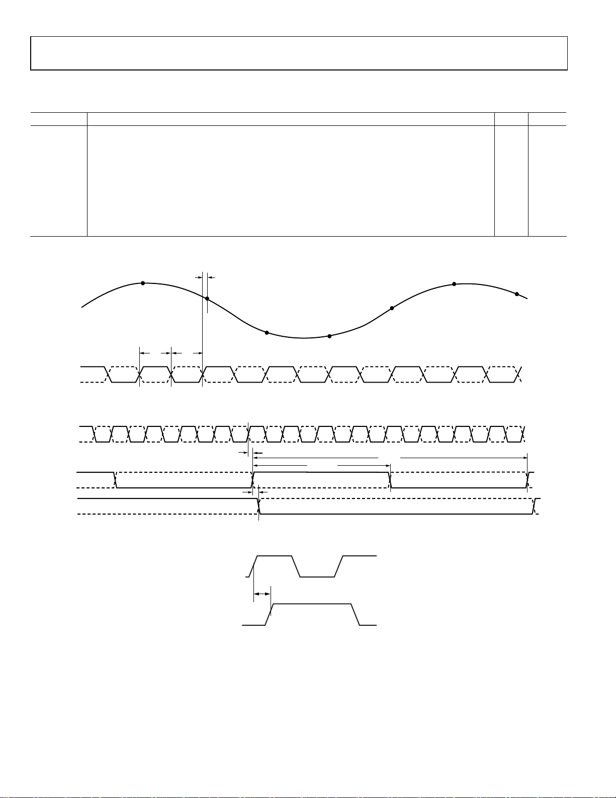
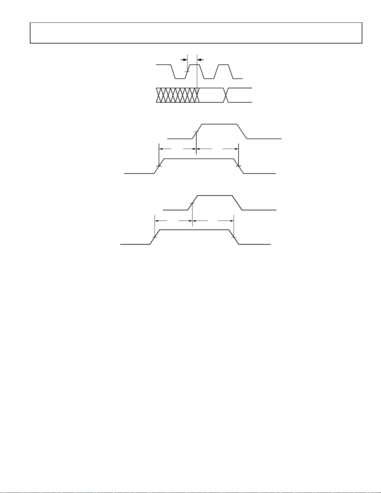
Timing Diagrams
VIN±
N–1
t
A
N
N+3
N+4
N+5
CLK+
CLK–
CLK+
CLK–
PCLK+
PCLK–
PD[11:0]
t
CH
OUTPUT DATA BUS
N+1
t
CL
Figure 2. Input Interface Timing
t
CPD
t
PCLK_CH
t
SKEW
Figure 3. Parallel CMOS Mode Output Interface Timing
SP_SCLK
t
DSDFS
SP_SDFS
Figure 4. SP_SDFS Propagation Delay
N+2
t
PCLK
09813-004
09813-002
09813-003
Rev. 0 | Page 8 of 28
Page 9
AD6641
SP_SCLK
SP_SDO D11 D10
t
DSDO
09813-005
Figure 5. SP_SDO Propagation Delay
SP_SCLK
SP_SDFS
t
SSF
t
HSF
09813-006
Figure 6. Slave Mode SP_SDFS Setup/Hold Time
CLK±
t
Sfill
t
Hfill
FILL±
09813-007
Figure 7. FILL± Setup and Hold Times
Rev. 0 | Page 9 of 28
Page 10

AD6641
ABSOLUTE MAXIMUM RATINGS
Table 6.
Parameter Rating
Electrical
AVDD to AGND −0.3 V to +2.0 V
DRVDD to DRGND −0.3 V to +2.0 V
AGND to DRGND −0.3 V to +0.3 V
AVDD to DRVDD −2.0 V to +2.0 V
SPI_VDDIO to AVDD −2.0 V to +2.0 V
SPI_VDDIO to DRVDD −2.0 V to +2.0 V
PD[5:0]± to DRGND −0.3 V to DRVDD + 0.2 V
PCLK± to DRGND −0.3 V to DRVDD + 0.2 V
PDOR± to DRGND −0.3 V to DRVDD + 0.2 V
FULL to DRGND −0.3 V to DRVDD + 0.2 V
CLK± to AGND −0.3 V to AVDD + 0.2 V
FILL± to AGND −0.3 V to DRVDD + 0.2 V
DUMP to AGND −0.3 V to DRVDD + 0.2 V
EMPTY to AGND −0.3 V to DRVDD + 0.2 V
VIN± to AGND −0.3 V to AVDD + 0.2 V
VREF to AGND −0.3 V to AVDD + 0.2 V
CML to AGND −0.3 V to AVDD + 0.2 V
CSB to DRGND −0.3 V to SPI_VDDIO + 0.3 V
SP_SCLK, SP_SDFS to AGND −0.3 V to SPI_VDDIO + 0.3 V
SDIO to DRGND −0.3 V to SPI_VDDIO + 0.3 V
SP_SDO to DRGND −0.3 V to SPI_VDDIO + 0.3 V
Environmental
Storage Temperature Range −65°C to +125°C
Operating Temperature Range −40°C to +85°C
Lead Temperature
(Soldering, 10 sec)
Junction Temperature 150°C
300°C
Stresses above those listed under Absolute Maximum Ratings
may cause permanent damage to the device. This is a stress
rating only; functional operation of the device at these or any
other conditions above those indicated in the operational
section of this specification is not implied. Exposure to absolute
maximum rating conditions for extended periods may affect
device reliability.
THERMAL RESISTANCE
The exposed pad must be soldered to the ground plane for
the LFCSP package. Soldering the exposed pad to the PCB
increases the reliability of the solder joints, maximizing the
thermal capability of the package.
Table 7.
Package Type θJA θ
56-Lead LFCSP_VQ (CP-56-1) 23.7 1.7 °C/W
Unit
JC
Typical θJA and θJC are specified for a 4-layer board in still air.
Airflow increases heat dissipation, effectively reducing θ
JA
. In
addition, metal in direct contact with the package leads from
metal traces, through holes, ground, and power planes reduces
the θ
.
JA
ESD CAUTION
Rev. 0 | Page 10 of 28
Page 11

AD6641
PIN CONFIGURATIONS AND FUNCTION DESCRIPTIONS
FULL
PCLK–
PCLK+
65
55
DNC
45
EMPTY
DUMP
35
25
FILL–
15
05
CLK–
AVDD
DRVDD
DRGND
FILL+
94
CLK+
AVDD
44
34
84
74
64
54
PD0–
PD0+
PD1–
PD1+
PD2–
PD2+
DRVDD
DRGND
PD3–
PD3+
10
PD4–
11
PD4+
12
13
PD5–
PD5+
14
NOTES
1. DNC = DO NOT CONNECT. DO NOT CONNECT TO THIS PIN.
2. THE EXPOSED PAD IS THE ONLY ANALOG GROUND
CONNECTION FOR THE CHIP. IT MUST BE CONNECTED TO PCB AGND.
PIN 1
1
INDICATOR
2
3
4
5
6
7
8
9
51
PDOR–
71
61
PDOR+
SP_SDO
AD6641
TOP VIEW
(Not to Scale)
12
81
02
22
91
DNC
DNC
DNC
SP_SDFS
SP_SCLK
52
42
32
SDIO
DRVDD
DRGND
72
62
CSB
SCLK
82
DNC
42
AVDD
41
AVDD
40
CML
39
AVDD
38
AVDD
37
AVDD
36
VIN–
35
VIN+
34
AVDD
33
AVDD
32
AVDD
31
VREF
30
AVDD
29
SPI_VDDIO
9813-008
Figure 8. Pin Configuration for DDR LVDS Mode
Table 8. DDR LVDS Mode Pin Function Descriptions
Pin No. Mnemonic Description
0 EPAD
Exposed Pad. The exposed pad is the only ground connection for the chip. The pad must be
connected to PCB AGND.
1 PD0− PD0 Data Output (LSB)—Complement.
2 PD0+ PD0 Data Output (LSB)—True.
3 PD1− PD1 Data Output—Complement.
4 PD1+ PD1 Data Output—True.
5 PD2− PD2 Data Output—Complement.
6 PD2+ PD2 Data Output—True.
7, 24, 47 DRVDD 1.9 V Digital Output Supply.
8, 23, 48 DRGND Digital Output Ground.
9 PD3− PD3 Data Output—Complement.
10 PD3+ PD3 Data Output—True.
11 PD4− PD4 Data Output—Complement.
12 PD4+ PD4 Data Output—True.
13 PD5− PD5 Data Output (MSB)—Complement.
14 PD5+ PD5 Data Output (MSB)—True.
15 PDOR− Overrange Output—Complement.
16 PDOR+ Overrange Output—True.
17 SP_SDO SPORT Output.
18, 19, 20, 28, 54 DNC Do Not Connect. Do not connect to this pin.
21 SP_SDFS SPORT Frame Sync Input (Slave Mode)/Output (Master Mode).
22 SP_SCLK SPORT Clock Input (Slave Mode)/Output (Master Mode).
25 SDIO Serial Port Interface (SPI) Data Input/Output (Serial Port Mode).
26 SCLK Serial Port Interface Clock (Serial Port Mode).
27 CSB Serial Port Chip Select (Active Low).
29 SPI_VDDIO 1.9 V or 3.3 V SPI I/O Supply.
30, 32, 33, 34, 37, 38, 39,
AVDD 1.9 V Analog Supply.
41, 42, 43, 46
31 VREF Voltage Reference Input/Output. Nominally 0.75 V.
35 VIN+ Analog Input—True.
36 VIN− Analog Input—Complement.
Rev. 0 | Page 11 of 28
Page 12

AD6641
Pin No. Mnemonic Description
40 CML
44 CLK+ Clock Input—True.
45 CLK− Clock Input—Complement.
49 FILL+ FIFO Fill Input (LVDS)—True.
50 FILL− FIFO Fill Input (LVDS)—Complement.
51 FULL FIFO Full Output Indicator.
52 EMPTY FIFO Empty Output Indicator.
53 DUMP FIFO Readback Input.
55 PCLK− Data Clock Output—Complement.
56 PCLK+ Data Clock Output—True.
Common-Mode Output. Enabled through the SPI, this pin provides a reference for the optimized
internal bias voltage for VIN+ and VIN−.
Rev. 0 | Page 12 of 28
Page 13

AD6641
FULL
PCLK–
PCLK+
65
55
DNC
45
DUMP
35
EMPTY
25
05
15
CLK–
AVDD
DRVDD
DRGND
FILL–
FILL+
CLK+
AVDD
44
94
34
84
74
64
54
DNC
DNC
PD0
PD1
PD2
PD3
DRVDD
DRGND
PD4
PD5
PD6
PD7
PD8
PD9
1. DNC = DO NOT CONNECT . DO NOT CONNECT TO THIS PIN.
2. THE EXPOSED PAD IS THE ONLY ANALOG GROUND
CONNECTION FOR THE CHIP. IT MUST BE CONNECTED TO PCB AGND.
PIN 1
1
INDICATOR
2
3
4
5
6
7
8
9
10
11
12
13
14
61
51
PD10
71
PD11
SP_SDO
AD6641
TOP VIEW
(Not to Scale)
12
81
02
22
91
DNC
DNC
DNC
SP_SDFS
SP_SCLK
32
DRGND
42
DRVDD
52
SDIO
42
AVDD
AVDD
41
CML
40
39
AVDD
AVDD
38
37
AVDD
VIN–
36
VIN+
35
AVDD
34
33
AVDD
32
AVDD
31
VREF
30
AVDD
29
SPI_VDDIO
82
72
62
CSB
DNC
SCLK
09813-009
Figure 9. Pin Configuration for Parallel CMOS Mode
Table 9. Parallel CMOS Mode Pin Function Descriptions
Pin No. Mnemonic Description
0 EPAD
Exposed Pad. The exposed pad is the only ground connection for the chip. The pad must be
connected to PCB AGND.
1, 2, 18, 19, 20, 28, 54 DNC Do Not Connect. Do not connect to this pin.
3 PD0 PD0 Data Output.
4 PD1 PD1 Data Output.
5 PD2 PD2 Data Output.
6 PD3 PD3 Data Output.
7, 24, 47 DRVDD 1.9 V Digital Output Supply.
8, 23, 48 DRGND Digital Output Ground.
9 PD4 PD4 Data Output.
10 PD5 PD5 Data Output.
11 PD6 PD6 Data Output.
12 PD7 PD7 Data Output.
13 PD8 PD8 Data Output.
14 PD9 PD9 Data Output.
15 PD10 PD10 Data Output.
16 PD11 PD11 Data Output (MSB).
17 SP_SDO SPORT Output.
21 SP_SDFS SPORT Frame Sync Input (Slave Mode)/Output (Master Mode).
22 SP_SCLK SPORT Clock Input (Slave Mode)/Output (Master Mode).
25 SDIO Serial Port Interface (SPI) Data Input/Output (Serial Port Mode).
26 SCLK Serial Port Interface Clock (Serial Port Mode).
27 CSB Serial Port Chip Select (Active Low).
29 SPI_VDDIO 1.9 V or 3.3 V SPI I/O Supply.
30, 32, 33, 34, 37, 38, 39,
AVDD 1.9 V Analog Supply.
41, 42, 43, 46
31 VREF Voltage Reference Input/Output. Nominally 0.75 V.
35 VIN+ Analog Input—True.
36 VIN− Analog Input—Complement.
40 CML
Common-Mode Output. Enabled through the SPI, this pin provides a reference for the
optimized internal bias voltage for VIN+ and VIN−.
44 CLK+ Clock Input—True.
Rev. 0 | Page 13 of 28
Page 14

AD6641
Pin No. Mnemonic Description
45 CLK− Clock Input—Complement.
49 FILL+ FIFO Fill Input (LVDS)—True.
50 FILL− FIFO Fill Input (LVDS)—Complement.
51 FULL FIFO Full Output Indicator.
52 EMPTY FIFO Empty Output Indicator.
53 DUMP FIFO Readback Input.
55 PCLK− Data Clock Output—Complement.
56 PCLK+ Data Clock Output—True.
Rev. 0 | Page 14 of 28
Page 15

AD6641
TYPICAL PERFORMANCE CHARACTERISTICS
AVDD = 1.9 V, DRVDD = 1.9 V, rated sample rate, TA = 25°C, 1.5 V p-p differential input, AIN = −1 dBFS, unless otherwise noted.
–20
–40
0
500MSPS
30.4MHz @ –1.0dBFS
SNR: 64.9dB
ENOB: 10.7 BITS
SFDR: 87dBc
–20
–40
0
491.52MSPS
368.0MHz @ –1.0dBFS
SNR: 63.8dB
ENOB: 10.5 BITS
SFDR: 77dBc
–60
–80
AMPLITUDE (dBFS)
–100
–120
0 20 40 60 80 100 120
FREQUENCY (MHz)
140 160 180 200 220 240
Figure 10. 16k Point Single-Tone FFT; 500 MSPS, 30.4 MHz
0
500MSPS
100.4MHz @ –1.0dBFS
–20
–40
–60
–80
AMPLITUDE (dBFS)
–100
–120
0 20 40 60 80 100 120
FREQUENCY (MHz)
SNR: 64.9dB
ENOB: 10.6 BITS
SFDR: 86dBc
140 160 180 200 220 240
Figure 11. 16k Point Single-Tone FFT; 500 MSPS, 100.4 MHz
–60
–80
AMPLITUDE (dBFS)
–100
–120
0 20 40 60 80 100 120
09813-010
FREQUENCY (MHz)
140 160 180 200 220 240
09813-013
Figure 13. 16k Point Single-Tone FFT; 491.52 MSPS, 368.0 MHz
0
491.52MSPS
450.1MHz @ –1.0dBFS
–20
–40
–60
–80
AMPLITUDE (dBFS)
–100
–120
0 20 40 60 80 100 120
09813-011
FREQUENCY (MHz)
SNR: 63.3dB
ENOB: 10.4 BITS
SFDR: 76dBc
140 160 180 200 220 240
09813-014
Figure 14. 16k Point Single-Tone FFT; 491.52 MSPS, 450.1 MHz
0
500MSPS
140.4MHz @ –1.0dBFS
–20
–40
–60
–80
AMPLITUDE (dBFS)
–100
–120
0 20 40 60 80 100 120
FREQUENCY (MHz)
SNR: 64.7dB
ENOB: 10.6 BITS
SFDR: 84dBc
140 160 180 200 220 240
Figure 12. 16k Point Single-Tone FFT; 500 MSPS, 140.4 MHz
09813-012
Figure 15. Single-Tone SNR/SFDR vs. Input Frequency (f
Rev. 0 | Page 15 of 28
95
90
85
80
75
70
SNR/SFDR (MHz)
65
60
SNR (dBFS), +85°C
55
50
0 100 200 300 400 500
SFDR (dBc), –40°C
SFDR (dBc), +25°C
SNR (dBFS), –40°C
ANALOG INPUT FREQUENCY (MHz)
SFDR (dBc), +85°C
SNR (dBFS), +25°C
) and Temperature;
IN
500 MSPS
09813-015
Page 16

AD6641
95
90
85
80
75
70
SNR/SFDR (dB)
65
60
55
50
F
D
S
R
(
d
B
c
)
SFDR @ 30.3MHz, 1.8V
SFDR @ 30.3MHz, 1.9V
SFDR @ 100.3MHz, 1.8V
SFDR @ 100.3MHz, 1.9V
N
S
R
(
d
B
)
F
S
SNRFS @ 30.3MHz, 1.8V
SNRFS @ 30.3MHz, 1.9V
SNRFS @ 100.3MHz, 1.8V
SNRFS @ 100.3MHz, 1.9V
250 300 350 400 450 500 550
R
A
L
E
P
A
M
S
)
S
P
S
E
(
M
T
Figure 16. SNR/SFDR vs. Sample Rate and Supply
9813-116
0.5
0.4
0.3
0.2
0.1
0
DNL (LSB)
–0.1
–0.2
–0.3
–0.4
–0.5
–1 1023 2047 3071 4095
OUTPUT CODE
Figure 19. DNL; 500 MSPS
09813-019
100
90
SFDR (dBFS)
80
70
60
50
40
SNR/SFDR (dB)
30
20
10
0
–90 –80 –70 –60 –50 –40 –30 –20 –10 0
SNR (dBFS)
SFDR (dBc)
SNR (dB)
AMPLITUDE (dB)
SNRFS, 1.9V
SNR, 1.9V
SFDR, 1.9V
SFDRFS, 1.9V
SNRFS, 1.8V
SNR, 1.8V
SFDR, 1.8V
SFDRFS, 1.8V
Figure 17. SNR/SFDR vs. Input Amplitude; 500 MSPS,140.3 MHz
1.0
0.8
0.6
0.4
0.2
0
INL (LSB)
–0.2
–0.4
–0.6
–0.8
–1.0
–1 1023 2047 3071 4095
OUTPUT CODE
Figure 18. INL; 500 MSPS
09813-117
09813-018
2.5
2.0
1.5
1.0
NUMBER OF HITS (M)
0.5
0
N–3 N–2 N–1 N N+1 N+2
BINS
Figure 20. Grounded Input Histogram; 500 MSPS
491.52MSPS
f
IN1
f
IN2
SFDR: 85dBc
AMPLITUDE (dBFS)
–105
–120
0
–15
–30
–45
–60
–75
–90
25 50 75 100 125 150 175 200 225
FREQUENCY (MHz)
Figure 21. 16k Point Single-Tone FFT; 491.52 MSPS,
f
= 121.3 MHz, f
IN1
= 124.7 MHz
IN2
1.24 LSB rms
N+3 MORE
: 121.3MHz @ –7dBFS
: 124.7MHz @ –7dBFS
09813-020
09813-021
Rev. 0 | Page 16 of 28
Page 17

AD6641
m
120
90
100
80
60
SFDR (dB)
40
SFDR (dBc)
20
0
–90 –80 –70 –60 –50 –40 –30 –20 –10 0
IMD3 (dBFS)
SFDR (dBFS)
AMPLITUDE (dBFS)
SFDR, 1.9V
SFDRFS, 1.9V
IMD3FS, 1.9V
SFDR, 1.8V
SFDRFS, 1.8V
IMD3FS, 1.8V
Figure 22. Two-Tone SFDR vs. Input Amplitude;
500 MSPS, 119.2 MHz, 122.5 MHz
120
100
80
60
SFDR (dB)
40
SFDR (dBc)
20
0
–90 –80 –70 –60 –50 –40 –30 –20 –10 0
IMD3 (dBFS)
SFDR (dBFS)
AMPLITUDE (dBFS)
SFDR, 1.9V
SFDRFS, 1.9V
IMD3FS, 1.9V
SFDR, 1.8V
SFDRFS, 1.8V
IMD3FS, 1.8V
Figure 23. Two-Tone SFDR vs. Input Amplitude;
500 MSPS, 139.3 MHz, 141.3 MHz
09813-022
09813-023
85
80
75
70
65
SNR/SFDR (dB)
60
55
50
1.75 1.80 1.85 1.90 1.95 2.00
SFDR (dBc)
SNR (dBFS)
POWER SUPPLY (V)
Figure 24. SNR/SFDR vs. Power Supply
400
350
300
A)
250
200
150
CURRENT (
100
50
0
250 300 350 400 450 500 550
TOTAL POWER
I
AVD D
I
DRVDD
SAMPLE RATE (MSPS)
Figure 25. Current and Power vs. Sample Rate
800
700
600
500
400
300
200
100
0
09813-024
POWER (mW)
09813-025
Rev. 0 | Page 17 of 28
Page 18

AD6641
V
V
V
V
V
O
S
S
V
EQUIVALENT CIRCUITS
AVDD
CML
BOOST
AVDD
IN+
500
AVDD
IN–
SPI
CONTROLLED
500
Figure 26. DC Equivalent Analog Input Circuit
IN+
1.3pF
VIN–
Figure 27. AC Equivalent Analog Input Circuit
A
DD
AVDD AVDD
CLK+
OR
FILL+
0.9V
15k 15k
1k
A
IN+
A
IN–
09813-017
DC
CLK–
OR
FILL–
DRVDD
V+
UTPUT–
V–
09813-016
V–
OUTPUT+
V+
9813-110
Figure 30. LVDS Outputs (PDOR±, PD[5:0]±, PCLK±)
DRVDD
DVDD
CLK
350
30k
09813-129
Figure 31. Equivalent SCLK Input Circuit
DRVDD
CSB
DRVDD
30k
DRVDD
350
09813-127
Figure 28. Equivalent CLK± and FILL± Input Circuit
DRVDD
DRGND
09813-128
Figure 29. Equivalent PD[11:0], FULL, EMPTY, PCLK±, and
Figure 32. Equivalent CSB Input Circuit
DR
DD
DRVDD
DIO
30k
350
Figure 33. Equivalent SDIO Circuit
09813-130
CTRL
09813-131
SP_SDO Output Circuit
Rev. 0 | Page 18 of 28
Page 19

AD6641
DRVDD
350
SP_SDFS/
SP_SCLK
30k
MASTER/SLAVE
Figure 34. Equivalent SP_SDFS and SP_SCLK Circuit
CTRL
9813-132
AVD D
VREF
20k
(00)
(01)
(10)
(11)
SPI CTRL VREF SELECT
00: INTERNAL VREF
01: IMORT VREF
10: EXPORT VREF
11: NOT USED
NOT USED
09813-133
Figure 35. Equivalent VREF Circuit
Rev. 0 | Page 19 of 28
Page 20

AD6641
SPI REGISTER MAP
Table 10. Memory Map Register
Default
Addr.
(Hex) Parameter Name
Chip Configuration Registers
0x00 CHIP_PORT_CONFIG 0 LSB
0x01 CHIP_ID 8-bit chip ID, Bits[7:0] = 0xA0 Read
0x02 CHIP_GRADE 0 0 Speed grade:
Transfer Register
0xFF DEVICE_UPDATE [7:1] = 0000000 SW
ADC Functions
0x08 Modes 0 0 0 0 0 Internal power-down mode:
0x0D TEST_IO (For user-defined
0x14 OUTPUT_MODE 0 0 0 Output
Bit 7
(MSB) Bit 6 Bit 5 Bit 4 Bit 3 Bit 2 Bit 1
first
mode only, set
Bits[3:0] = 1000)
00 = Pattern 1 only
01 = toggle
Pattern 1/
Pattern 2
10 = toggle
Pattern 1/0000
11 = toggle
Pattern 1/
Pattern 2/0000
Soft
reset
10 = 500 MSPS
Reset
PN23
gen:
1 = on
0 = off
(default)
1 1 Soft
X1
Reset
PN9
gen: 1 =
on
0 = off
(default)
0 =
disable:
0 =
enable
(default)
1 =
disable
CMOS:
1 =
LVDS
(default)
reset
1
XX1 XX1
X
000 = normal (power-up, default)
Output test mode:
0000 = off (default)
0001 = midscale short
0100 = checkerboard output
0101 = PN23 sequence
0111 = one/zero word toggle
1000 = user defined
(format determined by OUTPUT_MODE)
Output
invert:
1 = on
0 = off
(default)
LSB first 0 0x18 The nibbles
001 = full power-down
010 = standby
011 = reserved
0010 = +FS short
0011 = −FS short
0110 = PN9
1001 = unused
1010 = unused
1011 = unused
1100 = unused
Data format select:
00 = offset binary
Bit 0
(LSB)
transfer
(default)
01 = twos
complement
10 = Gray code
11 = reserved
Value
(Hex)
only
Read
only
0x00 Synchro-
0x00 Determines
0x00 When set, the
0x08
Default
Notes/
Comments
should be
mirrored by
the user so
that LSB or
MSB first
mode
registers
correctly,
regardless of
shift mode.
Default is
unique chip
ID, different
for each
device. This is
a read-only
register.
Child ID
used to
differentiate
graded
devices.
nously
transfers data
from the
master shift
register to the
slave.
various
generic
modes of chip
operation.
test data is
placed on the
output pins in
place of
normal data.
Set pattern
values:
Pattern 1:
Reg 0x19,
Reg 0x1A
Pattern 2:
Reg 0x1B
Reg 0x1C.
Rev. 0 | Page 20 of 28
Page 21

AD6641
Default
Addr.
(Hex) Parameter Name
Bit 7
(MSB) Bit 6 Bit 5 Bit 4 Bit 3 Bit 2 Bit 1
0x15 OUTPUT_ADJUST [7:4] = 0000 LVDS
course
adjust:
0 =
3.5 mA
(default)
1 =
2.0 mA
0x16 OUTPUT_PHASE Output
[6:0] = 0000000 0x03
Bit 0
(LSB)
LVDS fine adjust:
001 = 3.50 mA
010 = 3.25 mA
011 = 3.00 mA
100 = 2.75 mA
101 = 2.50 mA
110 = 2.25 mA
111 = 2.00 mA
Value
(Hex)
0x00
clock
polarity:
1 =
inverted
0 =
normal
(default)
0x17 OUTPUT_DELAY 0 0 0 0 Output clock delay:
0 Shown as
0000 = 0
0001 = −1/10
0010 = −2/10
0011 = −3/10
0100 = reserved
0101 = +5/10
0110 = +4/10
0111 = +3/10
1000 = +2/10
1001 = +1/10
0x18 Input range VREF select:
00 = internal V
(20 kΩ pull-down)
01 = import V
(0.59 V to 0.80 V on
VREF pin)
10 = export V
11= not used
REF
REF
REF
0 Input voltage range setting (V):
11100 = 1.60
11101 = 1.58
11110 = 1.55
11111 = 1.52
00000 = 1.50
00001 = 1.47
00010 = 1.44
0
00011 = 1.42
00100 = 1.39
00101 = 1.36
00110 = 1.34
00111 = 1.31
01000 = 1.28
01001 = 1.26
01010 = 1.23
01011= 1.20
01100 = 1.18
0x19 USER_PATT1_LSB [7:0] 0 User Defined
0x1A USER_PATT1_MSB [7:0] 0 User Defined
0x1B USER_PATT2_LSB [7:0] 0 User Defined
0x1C USER_PATT2_MSB [7:0] 0 User Defined
Digital Controls
0x101 Fill control register Reserved Fill
input
pin
disable
Reserved LIFO
mode
FIFO fill mode:
01 = continuous
1x = reserved
0x102 FIFO Config [7:4] = reserved Dump
Reserved Standby
00 = single
after fill
Fill reset Dump Fill 0
0
reset
0x104 Fill count [7:0] 0x7F Number of
Default
Notes/
Comments
fractional
value of
sampling
clock period
that is
subtracted or
added to
initial t
SKEW
,
see Figure 3).
Pattern 1 LSB.
Pattern 1 MSB.
Pattern 2 LSB.
Pattern 2 MSB.
words to use
for fill or
dump.
Rev. 0 | Page 21 of 28
Page 22

AD6641
Default
Addr.
(Hex)
0x105 Settle Count0 [7:0] 0 LSBs settling
0x106 Settle Count1 [7:0] 0 MSBs settling
0x107 Dump control [7:3] = reserved 0 =
0x10A FIFO status [7:3] = reserved Over-
0x10B FIFO Dump Data0 [7:0] = LSBs 0 LSBs readback
0x10C FIFO Dump Data1 [7:4] = reserved [3:0] = MSBs 0 MSBs upper
0x10F Read Offset Data0 [7:0] = LSBs 0 LSBs offset to
0x110 Read Offset Data1 [7:6] = reserved [5:0] = MSBs 0 MSB’s offset.
0x111 PPORT control [7:5] = reserved Divide ratio = 2 × (bit word):
0x112 SPORT control [7:5] = reserved Divide ratio= 2 × (bit word):
0x13A FIFO test BIST [7:5] = reserved Sets the BIST mode for the FIFO:
1
X = don’t care.
Parameter Name
Bit 7
(MSB)
Bit 6 Bit 5 Bit 4 Bit 3 Bit 2 Bit 1
Readback mode:
slave
1 =
master
Empty Full 0
range
00100 = divide by 8 (default)
…
01111 = divide by 30
1xxxx = divide by 32
00100 = divide by 8 (default)
…
01111 = divide by 30
1xxxx = divide by 32
1xxx = reserved
0111 = reserved
0110 = 12'hFFF (−1 LSB)
0101 = 12'h001 (+1 LSB)
0100 = PN data
0011 = checkerboard (12'hAAA, 12'h555,
12'hAAA, … )
0010 = checkerboard (12'h555, 12'hAAA,
12'h555, … )
0001 = decrementing ramp
0000 = incrementing ramp
Bit 0
(LSB)
00 = off
01 = parallel
10 = SPORT
11 = reserved
FIFO
BIST
enable
Value
(Hex)
0 Customer
0x04 CMOS parallel
0x04 Serial port
0
Default
Notes/
Comments
time given to
ADC before
initiating fill.
time given to
ADC before
initiating fill.
drives
SP_SCLK,
SP_SDFS in
slave mode.
data.
four bits
readback
data.
RAM, allowing
subsegments
of data capture to be
read.
port divide
rate.
divide rate.
Rev. 0 | Page 22 of 28
Page 23

AD6641
THEORY OF OPERATION
The on-chip FIFO allows small snapshots of time to be captured
via the ADC and read back at a lower rate. This reduces the
constraints of signal processing by transferring the captured
data at an arbitrary time and at a much lower sample rate.
FIFO OPERATION
The capture of the data can be signaled through writes to the
SPI port by pulsing the FILL± pins. The transaction diagram
shown in Figure 36 illustrates the loading of the FIFO.
At Event 1, the FIFO is instructed to fill either by asserting the
FILL± pins or via a write to the SPI bits. FILL± pin operation
can be delayed by a programmable fill hold-off counter so that
the FIFO data can be surrounding a fill event. The FIFO then
loads itself with data. The number of samples of data is
determined by the SPI fill count register (0x104). This is an 8bit register with values from 0 to 255. The number of samples
placed in the FIFO is determined by the following equation:
Number of Samples = (FILL_CNT + 1) × 64
After the FIFO has begun filling at Event 2, the AD6641 asserts
a full flag to indicate that the FIFO has finished capturing data
and enters a wait state in which the device waits to receive the
dump instruction from the DUMP pin or the SPI.
After the data has been shifted (Event 4), the FIFO goes into the
idle state and waits for another fill command. During the idle
state, the ADC can optionally be placed into standby mode to
save power. If the ADC powers down in the idle state, initiating
a fill operation (Event 1) powers up the ADC. In this mode, the
ADC waits for settle count cycles (0x105, 0x106) before capturing
the data. Settle count is programmable from the SPI port and
1 2 3 4
EVENTS
allows the analog circuitry to stabilize before taking data. An
intelligent trade-off between speed of acquisition and accuracy
can be made by using this register.
The data can be read back through any of the three output interfaces at a low data rate, which further saves power. If the SPI or
SPORT is used to read back the data, the interface can require
as few as three pins. A full flag and an empty flag are provided
to signal the state of the FIFO. The FIFO status register (0x10A)
in the SPI also allows this to be monitored via software.
Single Capture Mode
The FIFO can be placed into single capture mode by writing the
FIFO fill mode bits in the fill control register (0x101[3:2]) to 00.
In the single capture mode, the user initiates a capture either by
driving the FILL± pins high or by initiating a fill command
through the SPI port by writing the standby after fill bit
(0x101[0]). This powers up the ADC (if needed) after a
programmable amount of time as determined by the SPI settle
count registers (0x105, 0x106). If Bit 0 of the 0x101 register in
the SPI is set, the ADC returns to standby mode after the
capture is complete.
Fill Pin Timing
A fill of the FIFO can be initiated by asserting the differential
FILL± pins. When a pulse is detected on the FILL± pins, the
FIFO is filled.
Dump Pin Timing
A readback of the FIFO can be initiated by asserting the DUMP
pin. When a logic high is detected on the DUMP pin, the FIFO
data is available through the chosen interface.
STATE
IDLE STATE
FILL+, FILL–
FILLING FIFO WITH DATA
CLK+
CLK–
CLK+
CLK–
DUMP
WAIT FOR DUMP (OPTIONAL)
Figure 36. On-Chip FIFO Transaction Timing Assuming Serial Port
Figure 37. FIFO Fill Timing
Figure 38. FIFO DUMP Timing
START SP_SCLK AND SP_SDFS SHIFT DATA
IDLE STATE
09813-035
09813-036
09813-034
Rev. 0 | Page 23 of 28
Page 24

AD6641
SPORT Master Mode (Single Capture)
Details of the transaction diagram for serial master mode are
shown in Figure 39 for single capture mode with the SDO
output. Clock cycles are approximate because the fill and dump
signals can be driven asynchronously. In this example, SCLK is
derived from the master clock with a divide by 8 programmed
from the SPI.
Fill Pulse (1)
The FIFO captures data after a fill signal (high level) is detected
on the rising edge of the sampling clock. In synchronous operation, a valid high level is accomplished by adhering to the setup
and hold times specified. For nonsynchronous control, the fill
signal can be widened to accommodate two or more clock
cycles to guarantee capture of a high level. Fill count (0x104) is
reset on the rising edge of the clock and is incremented on
subsequent clock cycles only after the fill signal returns low.
A new fill signal at any point during the capture resets the
counter and begins filling the FIFO.
Empty Signal (2)
After the FIFO state machine has begun loading data, the empty
signal goes low 24 clock cycles after the fill signal was last
sampled high.
Full Signal (3)
The full signal indicates when the FIFO has been filled and is
driven high when the number of samples specified has been
captured in the FIFO, where
Number of Samples = (FILL_CNT + 1) × 64
The time at which the full signal goes high is based on
(FILL_CNT + 1) × 64 + 13 clock cycles after the fill signal was
last sampled high.
1
FILL
2
EMPTY
3
FULL
4
DUMP
5
SCLK
SDFS
Dump Signal (4)—Transition to High
The dump signal initiates reading data from the FIFO. Dump is
enabled with a high level and should be initiated only after the
full signal goes high. The dump signal should be held high until
all data has been read out of the FIFO.
SCLK Signal (5)
The SCLK (serial clock) signal is configured as an output from
the device when in the master mode of operation. SCLK begins
cycling five ADC clock cycles after the dump signal is sampled
high and continues cycling up until one additional cycle after
the empty signal goes high. SCLK then remains low until the
next dump operation.
SDFS Signal (6)
The SDFS (serial data frame sync) signal is configured as an
output from the device when in the master mode of operation.
Frame synchronization begins 15 ADC clock cycles after the
dump signal is sampled.
Dump Signal (7)—Transition to Low
A dump signal transition to low is applied after data has been
read out of the FIFO.
Empty Signal (8)—Transition to High
The empty signal transitions to high after data has been output
from the FIFO based on the clock cycle count of (FILL_CNT +
1) × 64.
The transition occurs 76 ADC clock cycles after the last LSB(s)
of data have been output on the serial port.
8
7
6
SDO
Figure 39. SPORT Master Mode Transaction Diagram
Rev. 0 | Page 24 of 28
09813-037
Page 25

AD6641
Parallel Master Mode (Single Capture)
Details of the transaction diagram for parallel master mode are
shown in Figure 40 with the PD[11:0] output word. Clock cycles
are approximate because the fill and dump signals can be driven
asynchronously. In this example, PCLK± is derived from the
master clock with a divide by 8 programmed from the SPI.
Fill Pulse (1)
The FIFO captures data after a fill signal (high level) is detected
on the rising edge of the sampling clock. In synchronous operation, a valid high level is accomplished by adhering to the setup
and hold times specified. For nonsynchronous control, the fill
signal can be widened to accommodate two or more clock
cycles to guarantee capture of a high level. Fill count (0x104)
is reset on the rising edge of the clock and is incremented on
subsequent clock cycles only after the fill signal returns low. A
new fill signal at any point during the capture resets the counter
and begins filling the FIFO.
Empty Signal (2)
After the FIFO state machine has begun loading data, the
empty signal goes low 24 clock cycles after the fill signal was
last sampled high.
Full Signal (3)
The full signal indicates when the FIFO has been filled and is
driven high when the number of samples specified has been
captured in the FIFO, where
Number of Samples = (FILL_CNT + 1) × 64
The time at which the full signal goes high is based on
(FILL_CNT + 1) × 64 + 13 clock cycles after the fill signal was
last sampled high.
1
FILL
2
Dump Signal (4)—Transition to High
The dump signal initiates reading data from the FIFO. Dump is
enabled with a high level and should be initiated only after the
full signal goes high. The dump signal should be held high until
all data has been read out of the FIFO.
PCLK± Signal (5)
The PCLK± (parallel clock) signal is configured as an output
from the device. PCLK± begins cycling 71 ADC clock cycles
after the dump signal is sampled high. PCLK± goes low after
the last data is read out of the FIFO and remains low until the
next dump operation.
PD[11:0] Signal (6)
The PD (parallel data) output provides 12 data bits (PD[11:0])
th
at a maximum rate of 1/8
of the sampling clock. Data begins
after two PCLK± cycles (assuming the dump signal has been
sampled).
Dump Signal (7)—Transition to Low
A dump signal transition to low is applied after data has been
read out of the FIFO.
Empty Signal (8)—Transition to High
The empty signal transitions to high after data has been output
from the FIFO based on the clock cycle count of (FILL_CNT +
1) × 64. The transition occurs nine clock cycles after the last
PCLK± rising edge.
Continuous Capture Mode
The FIFO can be placed into continuous capture mode by writing the FIFO fill mode bits in the fill control register (0x101[3:2])
to 01. In the continuous capture mode, data is loaded continuously into the FIFO and the FILL± pins pulsing high is used to
stop the operation. This allows the history of the samples that
preceded an event to be captured.
8
EMPTY
FULL
DUMP
PCLK+
PCLK–
PD[11:0]
3
4
5
6
D0 D8
Figure 40. Parallel Mode Transaction Diagram
Rev. 0 | Page 25 of 28
D16
7
9813-038
Page 26

AD6641
FIFO OUTPUT INTERFACES
The FIFO data is available through one of three interfaces. The
data can be output on the serial data port (SPORT), the SPI
port, or a 12-bit CMOS interface. The data port chosen must be
selected from the SPI port before the data is read from the FIFO.
Only one interface can be chosen at a time. The SPORT and SPI
interfaces are powered via the SPI_VDDIO pin and can support
either 1.9 V or 3.3 V logic levels.
SPORT Interface
The SPORT consists of a clock (SP_SCLK) and frame sync
(SP_SDFS) signal. The SP_SCLK and SP_SDFS signals are
output from the AD6641 when the SPORT is configured as
a bus master and are input to the device when it is configured
as a slave port.
Serial Data Frame (Serial Bus Master)
The serial data transfer is initiated with SP_SDFS. In master
mode, the internal serial controller initiates SP_SDFS after the
dump input goes high requesting the data. SP_SDFS is valid for
one complete clock cycle prior to the data shift. On the next
clock cycle, the AD6641 begins shifting out the data stream.
CMOS Output Interface
The data stored in the FIFO can also be accessed via a 12-bit
parallel CMOS interface. The maximum output throughput
supported by the AD6641 is in the 12-bit CMOS mode and is
internally limited to 1/8
Therefore, the output maximum output data rate is 62.5 MHz
th
of the maximum input sample rate.
0
SP_SCLK
4 8 12 16 20 24 28
at a 500 MSPS input sample rate. See Figure 3 for the parallel
CMOS mode output interface timing diagram.
LVDS Output Interface
The AD6641 differential outputs conform to the ANSI-644
LVDS standard on default power-up. This can be changed to a
low power, reduced signal option similar to the IEEE 1596.3
standard using the SPI. This LVDS standard can further reduce
the overall power dissipation of the device, which reduces the
power by ~39 mW. The LVDS driver current is derived on chip
and sets the output current at each output equal to a nominal
3.5 mA. A 100 Ω differential termination resistor placed at the
LVDS receiver inputs results in a nominal ±350 mV differential
or 700 mV p-p swing at the receiver.
The AD6641 LVDS outputs facilitate interfacing with LVDS
receivers in custom ASICs and FPGAs that have LVDS capability
for superior switching performance in noisy environments.
Single point-to-point net topologies are recommended with a
100 Ω termination resistor placed as close to the receiver as
possible. No far-end receiver termination and poor differential
trace routing may result in timing errors. It is recommended
that the trace length be no longer than 24 inches and that the
differential output traces be kept close together and at equal
lengths.
The data on the LVDS output port is interleaved in a MSB/LSB
format. PCLK± is generated by dividing the ADC sample clock
by the programmed decimation rate (8 to 32, even divides). The
maximum rate of PCLK± is limited to 62.5 MHz.
SP_SDFS
SP_SDO
D1 D3D2
Figure 41. Data Output in Serial Bus Master Mode
9813-039
PCLK+
PCLK–
PD[5:0]±
D0[11:6]D0[5:0] D8[11:6]D8[5:0] D16[11:6]D16[5:0] D24[11:6]D24[5:0]X
LSB/MSB
D0 SAMPLE
Figure 42. DDR LVDS Output MSB/LSB Interleaving with Decimate by 8
LSB/MSB
D8 SAMPLE
09813-040
Rev. 0 | Page 26 of 28
Page 27

AD6641
ANALOG INPUT AND VOLTAGE REFERENCE
The analog input to the AD6641 is a differential buffer. For
best dynamic performance, match the source impedances
driving VIN+ and VIN− such that common-mode settling
errors are symmetrical. The analog input is optimized to provide
superior wideband performance and requires that the analog
inputs be driven differentially. SNR and SINAD performance
degrades significantly if the analog input is driven with a singleended signal.
A wideband transformer, such as Mini-Circuits® ADT1-1WT,
can provide the differential analog inputs for applications that
require a single-ended-to-differential conversion. Both analog
inputs are self-biased by an on-chip reference to a nominal 1.7 V.
An internal differential voltage reference creates positive and
negative reference voltages that define the 1.5 V p-p fixed span
of the ADC core. This internal voltage reference can be adjusted
by means of an SPI control.
VREF
The AD6641 VREF pin (Pin 31) allows the user to monitor the
on-board voltage reference or provide an external reference
(requires configuration through the SPI). The three optional
settings are internal V
export V
, and import V
REF
(pin is connected to 20 kΩ to ground),
REF
. Do not attach a bypass capacitor
REF
to this pin. VREF is internally compensated and additional
loading may impact performance.
CONFIGURATION USING THE SPI
Three pins define the SPI of the AD6641: SCLK, SDIO, and CSB
(see Tabl e 11 ). SCLK (a serial clock) is used to synchronize the
read and write data presented from and to the AD6641. SDIO
(serial data input/output) is a bidirectional pin that allows data
to be sent to and read from the internal memory map registers.
CSB (chip select) is an active low control that enables or disables
the read and write cycles.
Table 11. Serial Port Interface Pins
Pin Function
SCLK
Serial clock. Serial shift clock input. SCLK is used to
synchronize serial interface reads and writes.
SDIO
Serial data input/output. Bidirectional pin that serves
as an input or an output, depending on the instruction
being sent and the relative position in the timing frame.
CSB
Chip select (active low). This control gates the read and
write cycles.
The falling edge of the CSB pin, in conjunction with the rising
edge of the SCLK pin, determines the start of the framing. An
example of the serial timing can be found in Figure 43 (for
symbol definitions, see Tabl e 5).
CSB can be held low indefinitely, which permanently enables
the device; this is called streaming. CSB can stall high between
bytes to allow additional external timing. When CSB is tied
high, SPI functions are placed in high impedance mode.
During an instruction phase, a 16-bit instruction is transmitted.
The first bit of the first byte in a serial data transfer frame indicates
whether a read command or a write command is issued. Data
follows the instruction phase, and its length is determined by
the W0 and W1 bits. All data is composed of 8-bit words.
The instruction phase determines whether the serial frame is a
read or write operation, allowing the serial port to be used both
to program the chip and to read the contents of the on-chip
memory. If the instruction is a read operation, the serial data
input/output (SDIO) pin changes direction from an input to an
output at the appropriate point in the serial frame.
Data can be sent in MSB first mode or in LSB first mode. MSB
first is the default mode on power-up and can be changed via
the SPI port configuration register. For more information about
this and other features, see the AN-877 Application Note,
Interfacing to High Speed ADCs via SPI.
CSB
SCLK
SDIO
DON’T
CARE
DON’T
CARE
t
DS
t
S
R/W W1W0A12A11A10A9A8A7 D5D4D3D2D1D0
t
HIGH
t
DH
t
LOW
Figure 43. Serial Port Interface Timing Diagram
t
CLK
Rev. 0 | Page 27 of 28
t
H
DON’T CARE
DON’T CARE
09813 -073
Page 28

AD6641
0
0
OUTLINE DIMENSIONS
0.30
0.23
0.18
PIN 1
56
INDICATOR
1
BSC SQ
PIN 1
INDICATOR
8.00
0.60 MAX
43
42
0.60 MAX
6.25
6.10 SQ
5.95
14
15
0.25 MIN
030509-A
1.00
.85
.80
SEATING
PLANE
12° MAX
TOP
VIEW
0.80 MAX
0.65 TYP
0.50 BSC
COMPLIANT TO JEDEC STANDARDS MO-220-VLL D-2
7.75
BSC SQ
0.20 REF
0.50
0.40
0.30
0.05 MAX
0.02 NOM
COPLANARIT Y
0.08
29
28
EXPOSED
PAD
(BOTTOM VIEW)
6.50
REF
FOR PROPE R CONNECTION OF
THE EXPOSE D PAD, REFER TO
THE PIN CONF IGURATI ON AND
FUNCTION DESCRIPTI ONS
SECTION OF THIS DATA SHEET.
Figure 44. 56-Lead Lead Frame Chip Scale Package [LFCSP_VQ]
8 mm × 8 mm Body, Very Thin Quad
(CP-56-1)
Dimensions shown in millimeters
ORDERING GUIDE
Model1 Temperature Range Package Description Package Option
AD6641BCPZ-500 −40°C to +85°C 56-Lead Lead Frame Chip Scale Package [LFCSP_VQ] CP-56-1
AD6641BCPZRL7-500 −40°C to +85°C 56-Lead Lead Frame Chip Scale Package [LFCSP_VQ], 7” Tape and Reel CP-56-1
AD6641-500EBZ Evaluation Board
1
Z = RoHS Compliant Part.
©2011 Analog Devices, Inc. All rights reserved. Trademarks and
registered trademarks are the property of their respective owners.
D09813-0-4/11(0)
Rev. 0 | Page 28 of 28
 Loading...