

Page 1
Monolithic 16-Bit
www.BDTIC.com/ADI
FEATURES
Complete 16-bit digital-to-analog function
On-chip output amplifier
On-chip buried Zener voltage reference
±1 LSB integral linearity
15-bit monotonic over temperature
Microprocessor compatible
Serial or byte input
Double-buffered latches
Fast (40 ns) write pulse
Asynchronous clear (to 0 V) function
Serial output pin facilitates daisy-chaining
Unipolar or bipolar output
Low glitch: 15 nV-s
Low THD + N: 0.009%
GENERAL DESCRIPTION
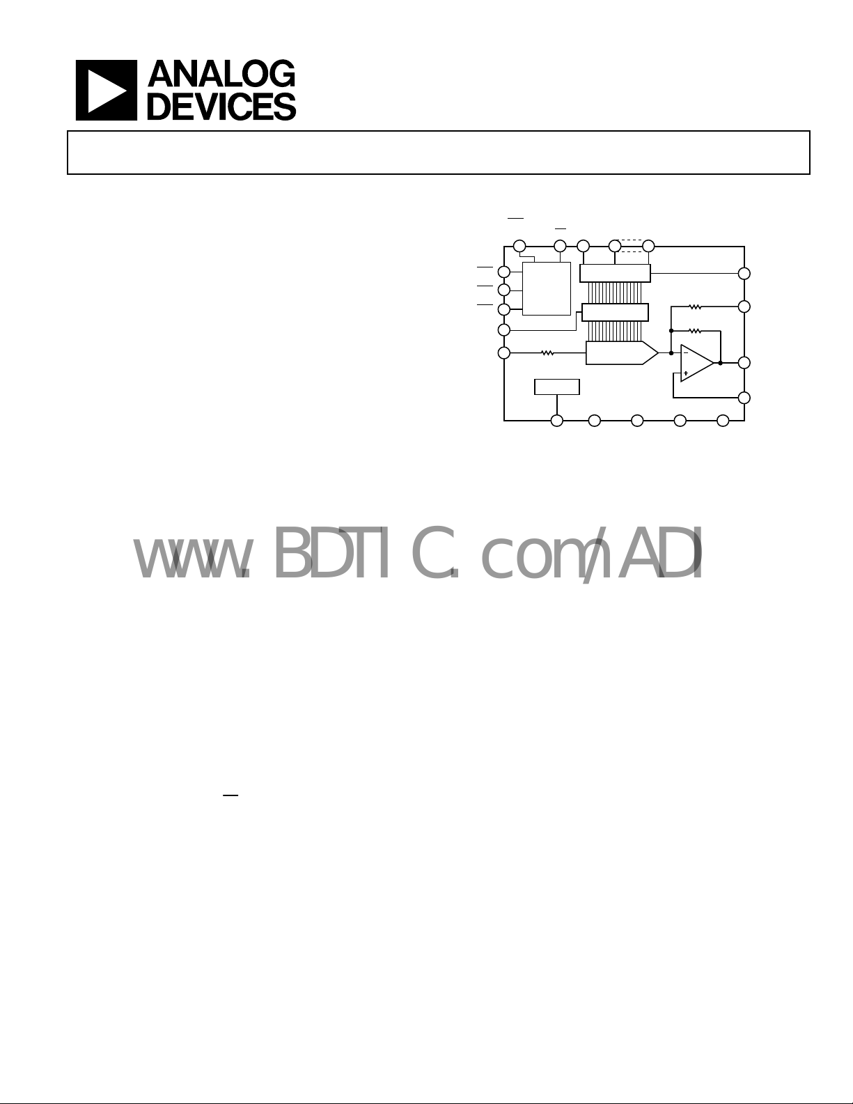
The AD660 DACPORT® is a complete 16-bit monolithic digitalto-analog converter with an on-board voltage reference, doublebuffered latches, and an output amplifier. It is manufactured on
the Analog Devices, Inc., BiMOS II process. This process allows
the fabrication of low power CMOS logic functions on the same
chip as high precision bipolar linear circuitry.
The AD660 architecture ensures 15-bit monotonicity over time
and temperature. Integral and differential nonlinearity is maintained at ±0.003% maximum. The on-chip output amplifier
provides a voltage output settling time of 10 μs to within ½ LSB for
a full-scale step.
The AD660 has an extremely flexible digital interface. Data can
be loaded into the AD660 in serial mode or as two 8-bit bytes.
This is made possible by two digital input pins that have dual
functions. The serial mode input format is pin selectable to be
MSB or LSB first. The serial output pin allows the user to daisychain several AD660 devices by shifting the data through the
input latch into the next DAC, thus minimizing the number of
control lines required to SIN,
format is also flexible in that the high byte or low byte data can
be loaded first. The double buffered latch structure eliminates
data skew errors and provides for simultaneous updating of DACs
in a multiDAC system.
The AD660 is available in five grades. AN and BN versions are
specified from −40°C to +85°C and are packaged in a 24-lead
300 mil plastic DIP. AR and BR versions are also specified from
−40°C to +85°C and are packaged in a 24-lead SOIC. The SQ
version is packaged in a 24-lead 300 mil CERDIP package and
CS
and LDAC. The byte mode input
Serial/Byte DACPORT
AD660
FUNCTIONAL BLOCK DIAGRAM
LOGIC
10kΩ
10V REF
24
REF OUT
DB0/
DB8/
DB1/DB9/
SIN
DATADIR
CS
121415
16-BIT LATCH
16-BIT LATCH
16-BIT DAC
1 2 3 4
–V
EE
11
+V
Figure 1.
DB15
CC
DB7/
5
AD660
10kΩ
10.05kΩ
+V
LL
DGND
13
22
21
20
S
OUT
SPAN/
BIPOL AR
OFFSET
V
OUT
AGND
LBE/
CLEAR SELECT
16
HBE
SER
CLR
LDAC
REF IN
17
18
19
23
CONTRO L
is also available compliant to MIL-STD-883. Refer to the
AD660SQ/883B military data sheet for specifications and test
conditions.
PRODUCT HIGHLIGHTS
1. The AD660 is a complete 16-bit DAC, with a voltage
reference, double-buffered latches, and an output amplifier
on a single chip.
2. The internal buried Zener reference is laser trimmed to
10.000 V with a ±0.1% maximum error and a temperature
drift performance of ±15 ppm/°C. The reference is available
for external applications.
3. The output range of the AD660 is pin programmable and
can be set to provide a unipolar output range of 0 V to 10 V
or a bipolar output range of −10 V to +10 V. No external
components are required.
4. The AD660 is both dc and ac specified. DC specifications
include ±1 LSB INL and ±1 LSB DNL errors. AC specifications include 0.009% THD + N and 83 dB SNR.
5. The double-buffered latches on the AD660 eliminate data
skew errors and allow simultaneous updating of DACs in
multiDAC applications.
6. The clear function can asynchronously set the output
to 0 V regardless of whether the DAC is in unipolar or
bipolar mode.
7. The output amplifier settles within 10 μs to ±½ LSB for a
full-scale step and within 2.5 μs for a 1 LSB step over temperature. The output glitch is typically 15 nV-s when a full-scale
step is loaded.
01813-001
Rev. B
Information furnished by Analog Devices is believed to be accurate and reliable. However, no
responsibility is assumed by Analog Devices for its use, nor for any infringements of patents or other
rights of third parties that may result from its use. Specifications subject to change without notice. No
license is granted by implication or otherwise under any patent or patent rights of Analog Devices.
Trademarks and registered trademarks are the property of their respective owners.
One Technology Way, P.O. Box 9106, Norwood, MA 02062-9106, U.S.A.
Tel: 781.329.4700 www.analog.com
Fax: 781.461.3113 ©1993–2008 Analog Devices, Inc. All rights reserved.
Page 2

AD660
www.BDTIC.com/ADI
TABLE OF CONTENTS
Features .............................................................................................. 1
Functional Block Diagram .............................................................. 1
General Description ......................................................................... 1
Product Highlights ........................................................................... 1
Revision History ............................................................................... 2
Specifications ..................................................................................... 3
AC Performance Characteristics ................................................ 4
Timing Characteristics ................................................................ 5
Absolute Maximum Ratings ............................................................ 7
ESD Caution .................................................................................. 7
Pin Configuration and Function Descriptions ............................. 8
Terminology ...................................................................................... 9
Theory of Operation ...................................................................... 10
Analog Circuit Connections ..................................................... 10
Unipolar Configuration ............................................................. 10
Bipolar Configuration ................................................................ 11
Internal/External Reference Use .............................................. 11
Output Settling and Glitch ........................................................ 13
Digital Circuit Details ................................................................ 14
Microprocessor Interface ............................................................... 15
AD660 to MC68HC11 (SPI Bus) Interface ............................. 15
AD660 to MICROWIRE Interface ........................................... 15
AD660 to ADSP-210x Family Interface .................................. 15
AD660 to Z80 Interface ............................................................. 16
Noise ............................................................................................ 16
Board Layout ................................................................................... 17
Supply Decoupling ..................................................................... 17
Grounding ................................................................................... 17
Outline Dimensions ....................................................................... 18
Ordering Guide .......................................................................... 19
REVISION HISTORY
6/08—Rev. A to Rev. B
Updated Format .................................................................. Universal
Updated Pin Name MSB/
Updated Pin Name
Throughout ....................................................................................... 1
Changes to Table 1 ............................................................................ 3
Changes to Endnote 3 in Table 1 .................................................... 4
Changes to Figure 2 .......................................................................... 5
Changes to Figure 3 and Figure 5 ................................................... 6
LSB
to DATADIR Throughout ........... 1
UNI
/BIP CLEAR to CLEAR SELECT
Changes to Table 4 ............................................................................. 7
Added Pin Configuration and Function Descriptions Section ... 8
Changes to Internal/External Reference Use Section ................ 11
Changes to Figure 12 ...................................................................... 12
Changes to Figure 13, Figure 14, Figure 15, and Figure 16....... 13
Changes to Figure 17 and Figure 18............................................. 15
Changes to Figure 19 ...................................................................... 16
Updated Outline Dimensions ....................................................... 18
Changes to Ordering Guide .......................................................... 19
Rev. B | Page 2 of 20
Page 3
AD660
www.BDTIC.com/ADI
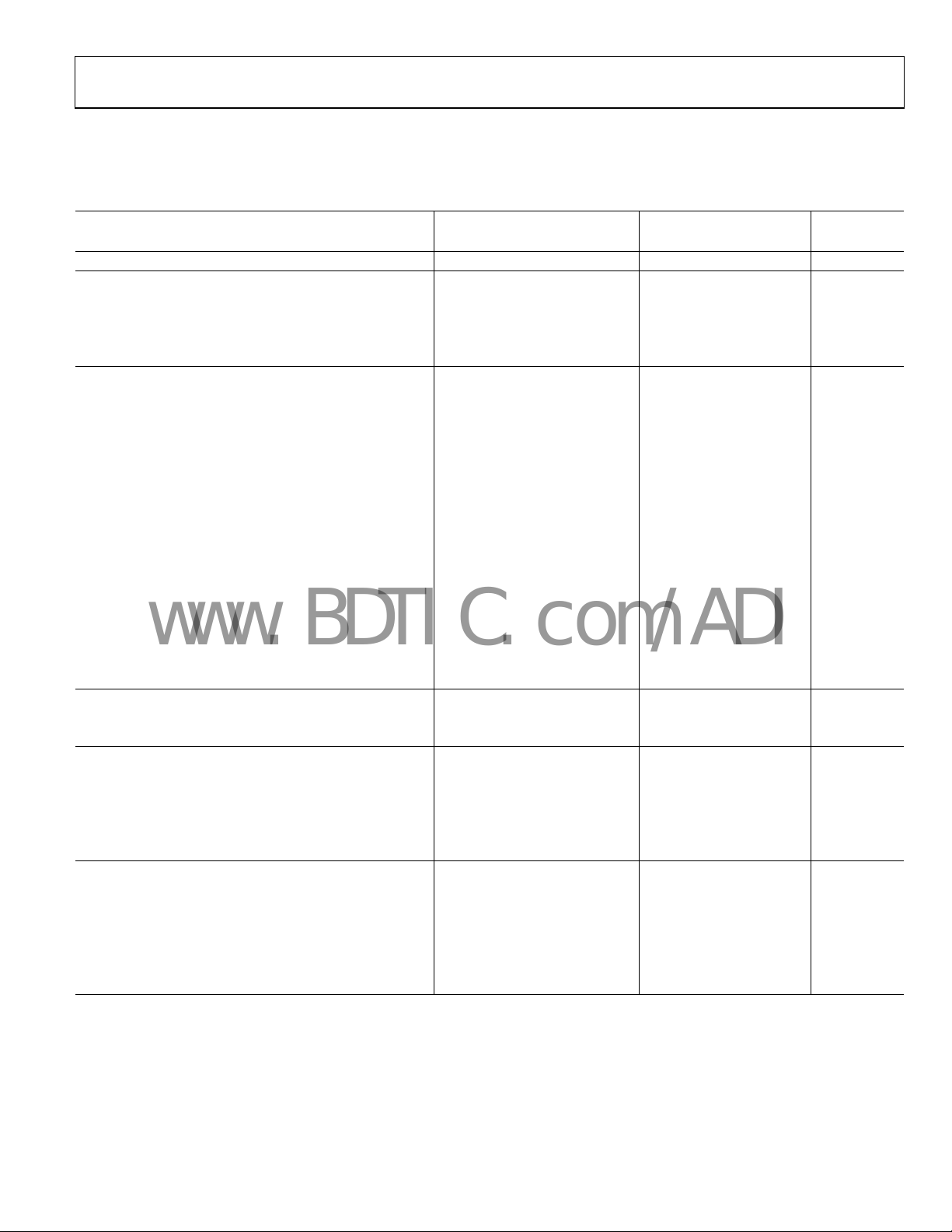
SPECIFICATIONS
TA = 25°C, +VCC = 15 V, −VEE = −15 V, +VLL = 5 V unless otherwise noted.
Table 1.
AD660AN/AR/SQ AD660BN/BR
Parameter
RESOLUTION 16 16 Bits
DIGITAL INPUTS (T
VIH (Logic 1) 2.0 5.5 2.0 5.5 V
VIL (Logic 0) 0 0.8 0 0.8 V
IIH (VIH = 5.5 V) −10 +10 −10 +10 μA
IIL (VIL = 0 V) −10 +10 −10 +10 μA
TRANSFER FUNCTION CHARACTERISTICS1
Integral Nonlinearity
Bipolar Operation −2 +2 −1 +1 LSB
T
to T
MIN
Unipolar Operation −2 +2 −1 +1.5 LSB
T
to T
MIN
Differential Nonlinearity −2 +2 −1 +1 LSB
T
to T
MIN
MAX
Monotonicity Over Temperature 14 15 Bits
Gain Error
Gain Drift (T
DAC Gain Error4 −0.05 +0.05 −0.05 +0.05 % of FSR
DAC Gain Drift4 10 10 ppm/°C
Unipolar Offset −2.5 +2.5 −2.5 +2.5 mV
Unipolar Offset Drift (T
Bipolar Zero Error −7.5 +7.5 −7.5 +7.5 mV
Bipolar Zero Error Drift (T
REFERENCE INPUT
Input Resistance 7 10 13 7 10 13 kΩ
Bipolar Offset Input Resistance 7 10 13 7 10 13 kΩ
REFERENCE OUTPUT
Voltage 9.99 10.00 10.01 9.99 10.00 10.01 V
Drift 25 15 ppm/°C
External Current5 2 4 2 4 mA
Capacitive Load 1000 1000 pF
Short-Circuit Current 25 25 mA
OUTPUT CHARACTERISTICS
Output Voltage Range
Output Current 5 5 mA
Capacitive Load 1000 1000 pF
Short-Circuit Current 25 25 mA
2, 3
Unipolar Configuration 0 +10 0 +10 V
Bipolar Configuration −10 +10 −10 +10 V
to T
MIN
−4 +4 −2 +2 LSB
MAX
−4 +4 −2 +2 LSB
MAX
−4 +4 −2 +2 LSB
to T
MIN
)
MAX
−0.1 +0.1 −0.1 +0.1 % of FSR
) 25 15 ppm/°C
MAX
to T
MIN
) 3 3 ppm/°C
MAX
to T
MIN
) 5 5 ppm/°C
MAX
Unit Min Typ Max Min Typ Max
Rev. B | Page 3 of 20
Page 4
AD660
www.BDTIC.com/ADI
AD660AN/AR/SQ AD660BN/BR
Parameter
POWER SUPPLIES
Voltage
6
+V
+13.5 +16.5 +13.5 +16.5 V
CC
6
−V
−13.5 −16.5 −13.5 −16.5 V
EE
+VLL +4.5 +5.5 +4.5 +5.5 V
Current (No Load)
ICC +12 +18 +12 +18 mA
IEE −12 −18 −12 −18 mA
ILL
@ VIH = 5 V, VIL = 0 V 0.3 2 0.3 2 mA
@ VIH = 2.4 V, VIL = 0.4 V 3 7.5 3 7.5 mA
Power Supply Sensitivity 1 2 1 2 ppm/%
Power Dissipation (Static, No Load) 365 625 365 625 mW
TEMPERATURE RANGE
Specified Performance (A, B) −40 +85 −40 +85 °C
Specified Performance (S) −55 +125 °C
1
For 16-bit resolution, 1 LSB = 0.0015% of FSR. For 15-bit resolution, 1 LSB = 0.003% of FSR. For 14-bit resolution, 1 LSB = 0.006% of FSR. FSR stands for full-scale range
and is 10 V in a unipolar mode and 20 V in bipolar mode.
2
Gain error and gain drift are measured using the internal reference. The internal reference is the main contributor to gain drift. If lower gain drift is required, the AD660
can be used with a precision external reference such as the AD587, AD586, or AD688.
3
Gain error is measured with fixed 50 Ω resistors as shown in the Theory of Operation section. Eliminating these resistors increases the gain error by 0.25% of FSR
(unipolar mode) or 0.50% of FSR (bipolar mode).
4
DAC gain error and drift are measured with an external voltage reference. They represent the error contributed by the DAC alone, for use with an external reference.
5
External current is defined as the current available in addition to that supplied to REF IN and SPAN/BIPOLAR OFFSET on the AD660.
6
Operation on ±12 V supplies is possible using an external reference such as the AD586 and reducing the output range. Refer to the Internal/External Reference Use
section.
Unit Min Typ Max Min Typ Max
AC PERFORMANCE CHARACTERISTICS
With the exception of total harmonic distortion + noise (THD + N) and signal-to-noise (SNR) ratio, these characteristics are included for
design guidance only and are not subject to test. THD + N and SNR are 100% tested.
T
≤ TA ≤ T
MIN
Table 2.
Parameter Limit Unit Test Conditions/Comments
OUTPUT SETTLING TIME 13 μs max 20 V step, TA = 25°C
(Time to ±0.0008% FS 8 μs typ 20 V step, TA = 25°C
with 2 kΩ, 1000 pF Load) 10 μs typ 20 V step, T
6 μs typ 10 V step, TA = 25°C
8 μs typ 10 V step, T
2.5 μs typ 1 LSB step, T
TOTAL HARMONIC DISTORTION + NOISE
A, B, S Grade 0.009 % max 0 dB, 990.5 Hz, sample rate = 96 kHz, TA = 25°C
A, B, S Grade 0.056 % max −20 dB, 990.5 Hz, sample rate = 96 kHz, TA = 25°C
A, B, S Grade 5.6 % max −60 dB, 990.5 Hz, sample rate = 96 kHz, TA = 25°C
SIGNAL-TO-NOISE RATIO 83 dB min TA = 25°C
DIGITAL-TO-ANALOG GLITCH IMPULSE 15 nV-s typ DAC alternately loaded with 0x8000 and 0x7FFF
DIGITAL FEEDTHROUGH 2 nV-s typ
OUTPUT NOISE VOLTAGE
Density (1 kHz to 1 MHz) 120 nV/√Hz typ Measured at V
REFERENCE NOISE 125
, +VCC = 15 V, −VEE = −15 V, +VLL = 5 V except where noted.
MAX
nV/√Hz typ Measured at REF OUT
≤ TA ≤ T
MIN
≤ TA ≤ T
MIN
MIN
≤ TA ≤ T
MAX
MAX
MAX
DAC alternately loaded with 0x0000 and 0xFFFF, CS
, 20 V span, excludes reference
OUT
high
Rev. B | Page 4 of 20
Page 5
AD660
www.BDTIC.com/ADI
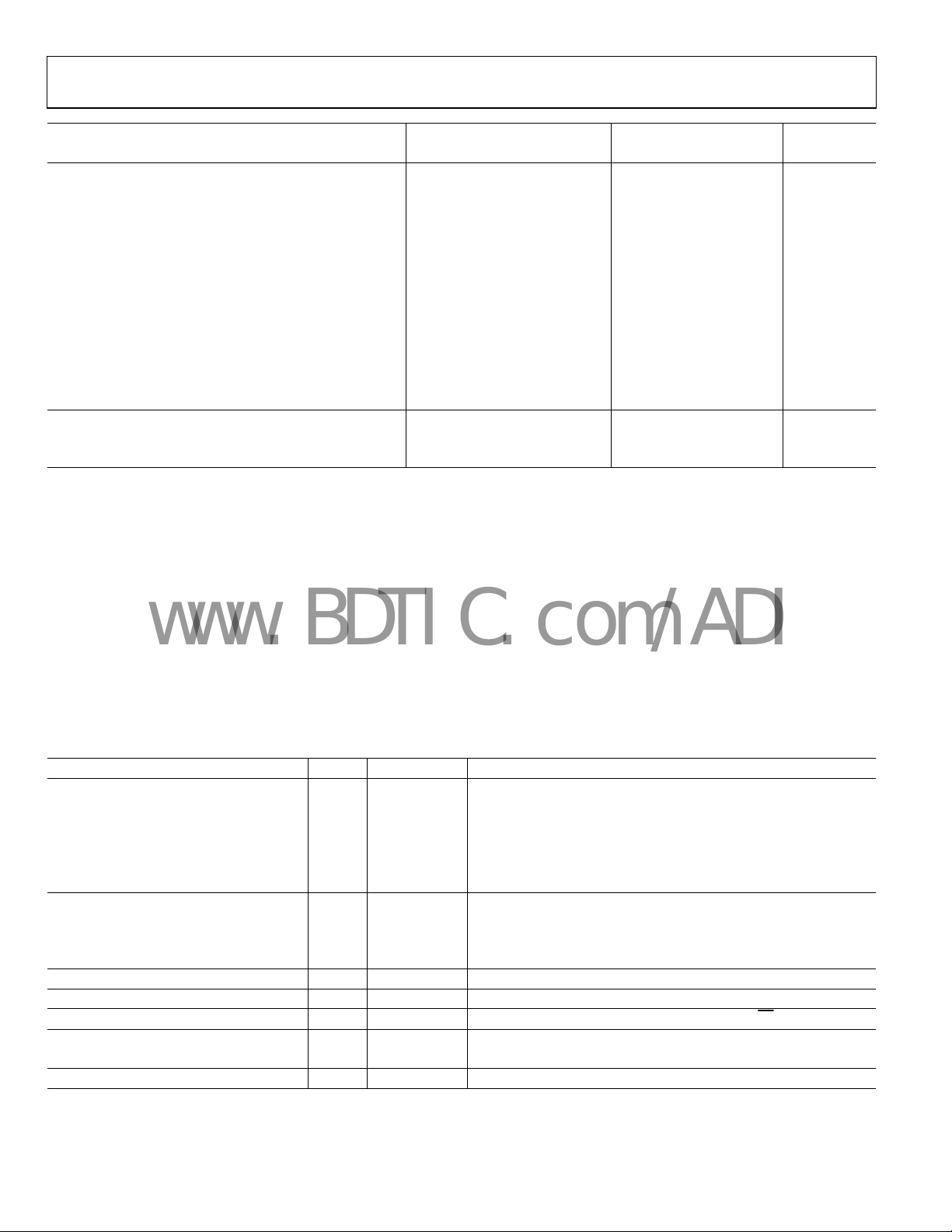
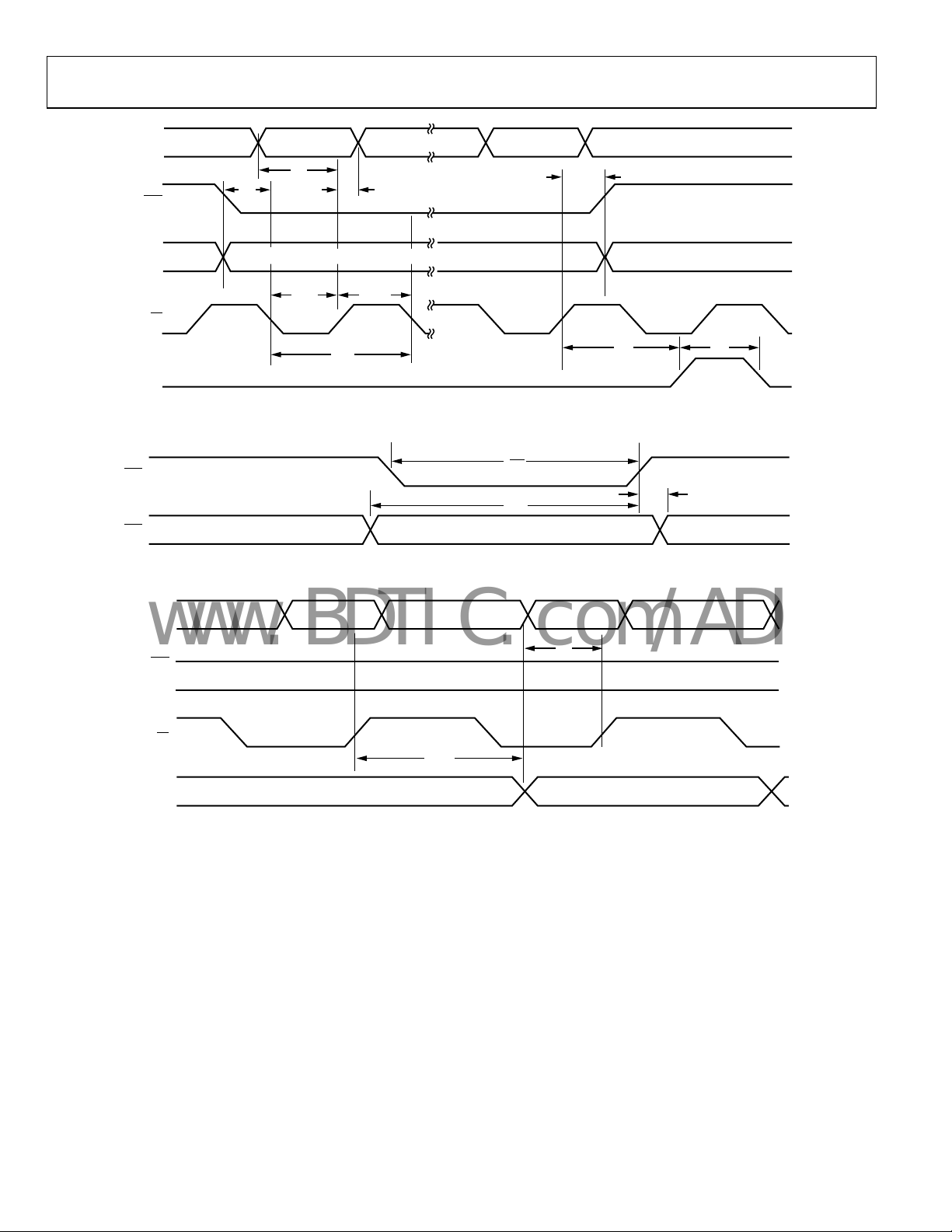
TIMING CHARACTERISTICS
+VCC = 15 V, −VEE = −15 V, +VLL = 5 V, V
Table 3.
Parameter Limit at TA = 25°C Limit at TA = −55°C to +125°C Unit
BYTE LOAD (see Figure 2)
tCS
tDS 40 50 ns min
tDH 0 10 ns min
t
40 50 ns min
BES
t
0 10 ns min
BEH
tLH 80 100 ns min
tLW 40 50 ns min
SERIAL LOAD (see Figure 3)
t
80 100 ns min
CLK
t
30 50 ns min
LOW
t
30 50 ns min
HIGH
tSS 0 10 ns min
tDS 40 50 ns min
tDH 0 10 ns min
tSH 0 10 ns min
tLH 80 100 ns min
tLW 40 50 ns min
ASYNCHRONOUS CLEAR TO BIPOLAR
OR UNIPOLAR ZERO (see Figure 4)
t
CLR
t
80 110 ns min
SET
t
0 10 ns min
HOLD
SERIAL OUT (see Figure 5)
t
50 100 ns min
PROP
tDS 50 80 ns min
= 2.4 V, V
HIGH
= 0.4 V.
LOW
40 50 ns min
80 110 ns min
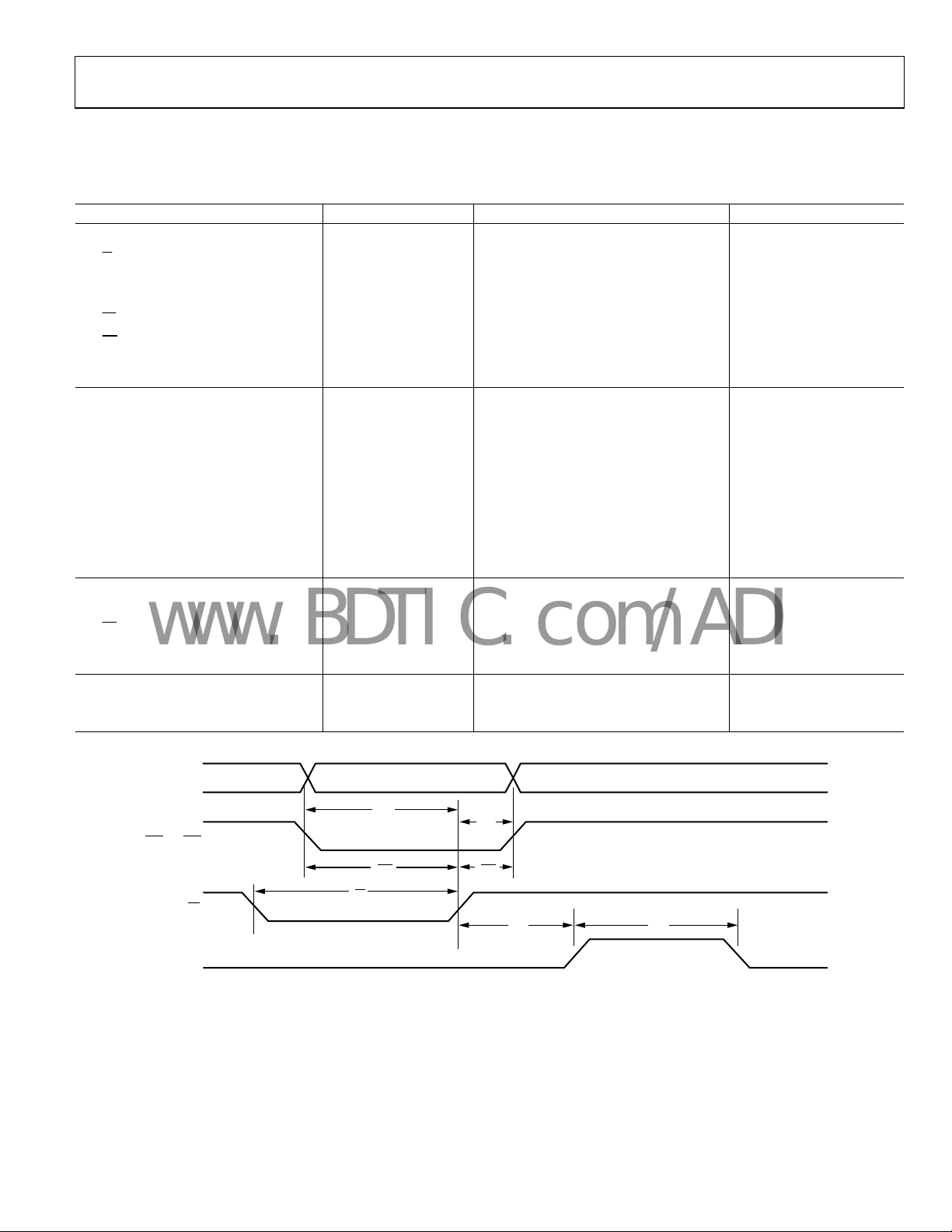
DB0 TO DB7
t
HBE OR LBE
CS
LDAC
DS
t
BES
t
CS
Figure 2. AD660 Byte Load Timing
t
DH
t
BEH
t
LH
Rev. B | Page 5 of 20
t
LW
01813-002
Page 6
AD660
C
(
www.BDTIC.com/ADI
DB0 VALID 1
t
SER
DB1
(DATADIR)
LDAC
CS
SS
t
DS
t
DH
1 = MSB FIRST, 0 = LSB FIRST
t
LOW
t
HIGH
t
CLK
VAL I D 1 6
t
SH
t
LH
t
LW
01813-003
Figure 3. AD660 Serial Load Timing
t
CLR
t
t
SET
HOLD
01813-004
LBE
LR
1 = BIPOLAR 0, 0 = UNIPOLAR 0
Figure 4. Asynchronous Clear to Bipolar or Unipolar Zero
DB0
SER
DB1
DATADIR)
CS
S
OUT
VALID 16 VALID 17
t
DS
t
PROP
VAL I D S
OUT
1
01813-005
Figure 5. Serial Out Timing
Rev. B | Page 6 of 20
Page 7

AD660
www.BDTIC.com/ADI
ABSOLUTE MAXIMUM RATINGS
Table 4.
Parameter Rating
+VCC to AGND −0.3 V to +17.0 V
−VEE to AGND +0.3 V to −17.0 V
+VLL to DGND −0.3 V to +7 V
AGND to DGND ±1 V
Digital Inputs (Pin 5 through Pin 23)
to DGND
REF IN to AGND ±10.5 V
SPAN/BIPOLAR OFFSET to AGND ±10.5 V
REF OUT, V
Power Dissipation (Any Package)
To +60°C 1000 mW
Derates Above +60°C 8.7 mW/°C
Storage Temperature −65°C to +150°C
Lead Temperature JEDEC industry standard
Soldering J-STD-020
OUT
−1.0 V to +7.0 V
Indefinite short to AGND,
DGND, +VCC, −VEE, and +VLL
Stresses above those listed under Absolute Maximum Ratings
may cause permanent damage to the device. This is a stress
rating only; functional operation of the device at these or any
other conditions above those indicated in the operational
section of this specification is not implied. Exposure to absolute
maximum rating conditions for extended periods may affect
device reliability.
ESD CAUTION
Rev. B | Page 7 of 20
Page 8

AD660
www.BDTIC.com/ADI
PIN CONFIGURATION AND FUNCTION DESCRIPTIONS
–V
+V
+V
DGND
DB7/DB15
DB6/DB14
DB5/DB13
DB4/DB12
DB3/DB 11
DB2/DB10
DB1/DB9/DATADIR
DB0/DB8/SIN
EE
CC
LL
1
2
3
4
AD660
5
TOP VIEW
6
(Not to Scale)
7
8
9
10
11
12
REF OUT
24
23
REF IN
SPAN/BIPOLAR OFFSET
22
21
V
OUT
AGND
20
19
LDAC
CLR
18
SER
17
HBE
16
LBE/CLEAR SELECT
15
14
CS
S
13
OUT
1813-006
Figure 6. Pin Configuration
Table 5. Pin Function Descriptions
Pin No. Mnemonic Description
1 −VEE Negative Analog Supply Pin
2 +VCC Positive Analog Supply Pin
3 +VLL Digital Supply Pin
4 DGND Digital Ground Reference Pin
5 DB7/DB15 DB7 and DB15 Byte Load Data Input Pin
6 DB6/DB14 DB6 and DB14 Byte Load Data Input Pin
7 DB5/DB13 DB5 and DB13 Byte Load Data Input Pin
8 DB4/DB12 DB4 and DB12 Byte Load Data Input Pin
9 DB3/DB11 DB3 and DB11 Byte Load Data Input Pin
10 DB2/DB10 DB2 and DB10 Byte Load Data Input Pin
11 DB1/DB9/DATADIR
DB1 and DB9 Byte Load Data Input Pin/MSB or LSB
First Data Direction Serial Input Select Pin
12 DB0/DB8/SIN DB0 and DB8 Byte Load Data Input Pin/Serial Data Input Pin
13 S
14
15
16
17
18
Serial Data Output Pin
OUT
CS
/CLEAR SELECT Low Byte Enable Pin/Unipolar or Bipolar Clear Select Pin
LBE
HBE
SER
CLR
Chip Select Pin
High Byte Enable Pin
Serial Input Enable Pin
Output Clear Pin
19 LDAC Load DAC Pin
20 AGND Analog Ground Reference Pin
21 V
Voltage Output Pin
OUT
22 SPAN/BIPOLAR OFFSET Output Span Configuration Pin
23 REF IN External Reference Voltage Input Pin
24 REF OUT Internal Reference Voltage Output Pin
Rev. B | Page 8 of 20
Page 9

AD660
www.BDTIC.com/ADI
TERMINOLOGY
Integral Nonlinearity
Integral nonlinearity is the maximum deviation of the actual,
adjusted DAC output from the ideal analog output (a straight
line drawn from 0 to FS − 1 LSB) for any bit combination. This
is also referred to as relative accuracy.
Differential Nonlinearity
Differential nonlinearity is the measure of the change in the
analog output, normalized to full scale, associated with a 1 LSB
change in the digital input code. Monotonic behavior requires
that the differential linearity error be greater than or equal to
−1 LSB over the temperature range of interest.
Monotonicity
A DAC is monotonic if the output either increases or remains
constant for increasing digital inputs with the result that the
output is always a single-valued function of the input.
Gain Error
Gain error is a measure of the output error between an ideal
DAC and the actual device output with all 1s loaded after offset
error has been adjusted out.
Offset Error
Offset error is a combination of the offset errors of the voltagemode DAC and the output amplifier and is measured with all 0s
loaded in the DAC.
Bipolar Zero Error
When the AD660 is connected for bipolar output and 10…000
is loaded in the DAC, the deviation of the analog output from
the ideal midscale value of 0 V is called the bipolar zero error.
Drift
Drift is the change in a parameter (such as gain, offset, and bipolar
zero) over a specified temperature range. The drift temperature
coefficient, specified in ppm/°C, is calculated by measuring the
parameter at T
the parameter by the corresponding temperature change.
Total Harmonic Distortion + Noise
Total harmonic distortion + noise (THD + N) is defined as the
ratio of the square root of the sum of the squares of the values of
the harmonics and noise to the value of the fundamental input
frequency. It is usually expressed in percent (%).
THD + N is a measure of the magnitude and distribution of
linearity error, differential linearity error, quantization error,
and noise. The distribution of these errors may be different,
depending upon the amplitude of the output signal. Therefore,
to be the most useful, THD + N should be specified for both
large and small signal amplitudes.
Signal-To-Noise Ratio
The signal-to-noise ratio is the ratio of the amplitude of the output
when a full-scale signal is present to the output with no signal
present. The signal-to-noise ratio is measured in decibels (dB).
Digital-To-Analog Glitch Impulse
Digital-to-analog glitch impulse is the amount of charge
injected from the digital inputs to the analog output when the
inputs change state. This is measured at half scale when the DAC
switches around the MSB and as many as possible switches
change state, that is, from 011…111 to 100…000.
Digital Feedthrough
When the DAC is not selected (that is,
frequency logic activity on the digital inputs is capacitively
coupled through the device to show up as noise on the V
This noise is digital feedthrough.
, 25°C, and T
MIN
, and dividing the change in
MAX
CS
is held high), high
OUT
pin.
Rev. B | Page 9 of 20
Page 10

AD660
www.BDTIC.com/ADI
THEORY OF OPERATION
The AD660 uses an array of bipolar current sources with MOS
current steering switches to develop a current proportional to the
applied digital word, ranging from 0 mA to 2 mA. A segmented
architecture is used, where the most significant four data bits
are thermometer decoded to drive 15 equal current sources.
The lesser bits are scaled using a R-2R ladder, then applied
together with the segmented sources to the summing node of
the output amplifier. The internal span/bipolar offset resistor
can be connected to the DAC output to provide a 0 V to 10 V
span, or it can be connected to the reference input to provide a
−10 V to +10 V span.
LOGIC
10kΩ
10V REF
24
REF OUT
DB0/
DB8/
DB1/DB9/
CS
SIN
DATADIR
16-BIT LATCH
16-BIT LATCH
16-BIT DAC
1 2 3 4
–V
EE
DB7/
DB15
5
11121415
+V
CC
Figure 7. Functional Block Diagram
AD660
10kΩ
10.05kΩ
+V
LL
DGND
S
13
OUT
SPAN/
BIPOL AR
22
OFFSET
21
V
OUT
AGND
20
(Pin 21),
OUT
LBE/
CLEAR SELECT
16
HBE
SER
CLR
LDAC
REF IN
17
18
19
23
CONTRO L
ANALOG CIRCUIT CONNECTIONS
Internal scaling resistors provided in the AD660 can be connected
to produce a unipolar output range of 0 V to 10 V or a bipolar
output range of −10 V to +10 V. Gain and offset drift are minimized in the AD660 because of the thermal tracking of the
scaling resistors with other device components.
UNIPOLAR CONFIGURATION
The configuration shown in Figure 8 provides a unipolar 0 V to
10 V output range. In this mode, 50 Ω resistors are tied between
the SPAN/BIPOLAR OFFSET terminal (Pin 22) and V
and between REF OUT (Pin 24) and REF IN (Pin 23). It is possible
to use the AD660 without any external components by tying Pin 24
directly to Pin 23 and Pin 22 directly to Pin 21. Eliminating
these resistors increases the gain error by 0.25% of FSR.
LOGIC
10kΩ
10V REF
DB0/
DB1/DB9/
DB8/
CS
DATADIR
SIN
11
16-BIT LATCH
16-BIT LATCH
16-BIT DAC
24
1 2 3 4
–V
EE
DB7/
DB15
51214
AD660
S
OUT
13
SPAN/
10kΩ
10.05kΩ
+V
+V
CC
DGND
LL
BIPOLAR
OFFSET
22
V
21
AGND
20
R2
50Ω
OUT
OUTPUT
01813-008
CLEAR SELECT
HBE
SER
CLR
LDAC
REF IN
16
17
18
19
23
50Ω
LBE/
R1
15
CONTROL
REF OUT
Figure 8. 0 V to 10 V Unipolar Voltage Output
If it is desired to adjust the gain and offset errors to zero, this
can be accomplished using the circuit shown in Figure 9. The
adjustment procedure is as follows:
1. Zero adjust.
Turn all bits off and adjust the zero trimmer, R4, until the
output reads 0.000000 V (1 LSB = 153 μV).
2. Gain adjust.
Turn all bits on and adjust the gain trimmer, R1, until the
01813-007
output is 9.999847 V. (Full scale is adjusted to 1 LSB less
than the nominal full scale of 10.000000 V.)
LOGIC
10kΩ
10V REF
DB0/
DB8/
DB1/DB9/
CS
SIN
DATADIR
11
16-BIT LATCH
16-BIT LATCH
16-BIT DAC
24
1 2 3 4
–V
EE
Adjustment
DB7/
DB15
51214
AD660
S
OUT
13
SPAN/
BIPOLAR
OFFSET
10kΩ
10.05kΩ
+V
+V
CC
LL
22
21
20
DGND
R2
50Ω
V
OUT
OUTPUT
AGND
R3
16k
+V
CC
R4
10k
–V
EE
01813-009
LBE/
CLEAR SELECT
15
16
HBE
CONTRO L
17
SER
18
CLR
19
LDAC
REF IN
23
REF OUT
R1
100Ω
Figure 9. 0 V to 10 V Unipolar Voltage Output with Gain and Offset
Rev. B | Page 10 of 20
Page 11

AD660
www.BDTIC.com/ADI
BIPOLAR CONFIGURATION
The circuit shown in Figure 10 provides a bipolar output voltage
from −10.000000 V to +9.999694 V with positive full scale occurring with all bits on. As in the unipolar mode, Resistor R1 and
Resistor R2 can be eliminated altogether to provide AD660 bipolar
operation without any external components. Eliminating these
resistors increases the gain error by 0.50% of FSR in bipolar mode.
R2
50Ω
DB0/
DB8/
CLEAR SELECT
16
HBE
17
SER
18
CLR
19
LDAC
23
R1
50Ω
LBE/
15
REF IN
REF OUT
CONTROL
LOGIC
10kΩ
10V REF
24
DB1/DB9/
CS
SIN
DATADIR
16-BIT LATCH
16-BIT LATCH
16-BIT DAC
1 2 3 4
–V
EE
Figure 10. ±10 V Bipolar Voltage Output
Gain offset and bipolar zero errors can be adjusted to zero using
the circuit shown in Figure 11 as follows:
1. Offset adjust.
Turn off all bits. Adjust the trimmer, R2, to give 10.000000 V
output.
2. Gain adjust.
Turn all bits on and adjust R1 to give a reading of 9.999694 V.
3. Bipolar zero adjust (optional).
In applications where an accurate zero output is required, set
the MSB on, all other bits off, and readjust R2 for 0 V output.
11
DB7/
DB15
51214
+VCC+V
AD660
10kΩ
10.05kΩ
LL
DGND
S
13
22
SPAN/
BIPOLAR
OFFSET
V
OUT
21
AGND
20
OUT
OUTPUT
01813-010
R2
100Ω
DB0/
CLEAR SELECT
16
HBE
17
SER
18
CLR
19
LDAC
23
R1
50Ω
LBE/
15
REF IN
REF OUT
CS
CONTROL
LOGIC
10kΩ
10V REF
24
DB8/
DB1/DB9/
SIN
DATADIR
16-BIT LATCH
16-BIT LATCH
16-BIT DAC
1 2 3 4
–V
EE
11
DB7/
DB15
51214
+VCC+V
AD660
10kΩ
10.05kΩ
LL
DGND
S
OUT
13
22
SPAN/
BIPOLAR
OFFSET
V
OUT
21
AGND
20
OUTPUT
01813-011
Figure 11. ±10 V Bipolar Voltage Output with Gain and Offset Adjustment
Note that using external resistors introduces a small temperature
drift component beyond that inherent in the AD660. The internal resistors are trimmed to ratio-match and temperature-track
other resistors on-chip, even though their absolute tolerances are
±20% and absolute temperature coefficients are approximately
−50 ppm/°C. In the case that external resistors are used, the
temperature coefficient mismatch between internal and external
resistors, multiplied by the sensitivity of the circuit to variations
in the external resistor value, is the resultant additional temperature drift.
INTERNAL/EXTERNAL REFERENCE USE
The AD660 has an internal low noise buried Zener diode
reference that is trimmed for absolute accuracy and temperature
coefficient. This reference is buffered and optimized for use in a
high speed DAC and gives long-term stability equal or superior to
the best discrete Zener diode references. The performance of
the AD660 is specified with the internal reference driving the
DAC and with the DAC alone (for use with a precision external
reference).
The internal reference has sufficient buffering to drive external
circuitry in addition to the reference currents required for the
DAC (typically 1 mA to REF IN and 1 mA to SPAN/BIPOLAR
OFFSET). A minimum of 2 mA is available for driving external
loads. The AD660 reference output should be buffered with an
external op amp if it is required to supply more than 4 mA total
current. The reference is tested and guaranteed to ±0.2%
maximum error.
Rev. B | Page 11 of 20
Page 12

AD660
www.BDTIC.com/ADI
It is also possible to use external references other than 10 V with
slightly degraded linearity specifications. The recommended
range of reference voltages is 5 V to 10.24 V, which allows 5 V,
8.192 V, and 10.24 V ranges to be used. For example, by using
the AD586 5 V reference, outputs of 0 V to 5 V unipolar or ±5 V
bipolar can be realized. Using the AD586 voltage reference
makes it possible to operate the AD660 with ±12 V supplies
with 10% tolerances.
Figure 12 shows the AD660 using the AD586 precision 5 V
reference in the bipolar configuration. The highest grade
AD586MN is specified with a drift of 2 ppm/°C, which is a
7.5× improvement over the AD660 internal reference. This
circuit includes two optional potentiometers and one optional
resistor that can be used to adjust the gain, offset, and bipolar
R2
50Ω
LBE/
CLEAR SELECT
15
16
V
2
V
OUT
AD586
TRIM
GND
4
HBE
SER
R2
10kΩ
CLR
LDAC
R1
50Ω
IN
6
5
Figure 12. Using the AD660 with the AD586 5 V Reference
17
18
19
23
REF IN
CONTROL
LOGIC
10kΩ
10V REF
REF OUT
CS
24
zero errors in a manner similar to that described in the Bipolar
Configuration section. Use −5.000000 V and +4.999847, as the
output values.
The AD660 can also be used with the AD587 10 V reference,
using the same configuration shown in Figure 12 to produce a
±10 V output. The highest grade AD587UQ is specified at
5 ppm/°C, which is a 3× improvement over the AD660 internal
reference.
Figure 13 shows the AD660 using the AD688 precision
±10 V reference, in the unipolar configuration. The highest
grade AD688BQ is specified with a temperature coefficient of
1.5 ppm/°C. The ±10 V output is also ideal for providing precise
biasing for the offset trim resistor, R4.
DB0/
DB8/
DB1/DB9/
SIN
DATADIR
16-BIT LATCH
16-BIT LATCH
16-BIT DAC
1 2 3 4
–V
EE
11
DB7/
DB15
51214
+V
CC+VLL
AD660
10kΩ
10.05kΩ
DGND
S
13
22
SPAN/
BIPOLAR
OFFSET
V
OUT
21
AGND
20
OUT
OUTPUT
01813-012
Rev. B | Page 12 of 20
Page 13

AD660
www.BDTIC.com/ADI
R2
50Ω
DB0/
DB8/
CS
DB1/DB9/
SIN
DATADIR
16-BIT LATCH
16-BIT LATCH
16-BIT DAC
467 3
CLEAR SELECT
16
HBE
17
SER
18
CLR
19
LDAC
23
R1
50Ω
LBE/
15
REF IN
CONTROL
LOGIC
10kΩ
10V REF
AD688
24
R
A1
S
R4
R1
R2
R3
R5
A2
R6
13111281095
1
A3
14
15
A4
+V
2
S
16
–V
S
REF OUT
1 2 3 4
–V
EE
11
+VCC+V
DB7/
DB15
51214
AD660
10kΩ
10.05kΩ
LL
DGND
S
OUT
13
22
SPAN/
BIPOL AR
OFFSET
V
OUT
21
AGND
20
R3
10kΩ
R2
100Ω
R4
10kΩ
OUTPUT
0V TO 10V
01813-013
Figure 13. Using the AD660 with the AD688 High Precision ±10 V Reference
OUTPUT SETTLING AND GLITCH
The AD660 output buffer amplifier typically settles to within
0.0008% FS (1/2 LSB) of its final value in 8 μs for a full-scale
step. Figure 14 and Figure 15 show settling for a full-scale and
an LSB step, respectively, with a 2 kΩ, 1000 pF load applied.
The guaranteed maximum settling time at 25°C for a full-scale
step is 13 μs with this load. The typical settling time for a 1 LSB
step is 2.5 μs.
The digital-to-analog glitch impulse is specified as 15 nV-s
typical. Figure 16 shows the typical glitch impulse characteristic
at the 011…111 to 100…000 code transition when loading the
second rank register from the first rank register.
600
+10
0
OUTPUT VO LTAGE (V )
–10
01020
TIME (µs)
Figure 14. −10 V to +10 V Full-Scale Step Settling
400
200
0
–200
–400
–600
OUTPUT VOL TAGE (µV)
600
400
200
0
–200
OUTPUT VOL TAGE (µV)
–400
–600
01 2345
TIME (µs)
01813-015
Figure 15. LSB Step Settling
+10
0
OUTPUT VOLTAGE (mV)
–10
01813-014
01 23 45
TIME (µs)
01813-016
Figure 16. Output Characteristics
Rev. B | Page 13 of 20
Page 14

AD660
www.BDTIC.com/ADI
CLR
DIGITAL CIRCUIT DETAILS
The AD660 has several dual-use pins that allow flexible operation while maintaining the lowest possible pin count and
consequently the smallest package size. The user should,
therefore, pay careful attention to the following information
when applying the AD660.
Data can be loaded into the AD660 in serial or byte mode,
described as follows.
Serial mode operation is enabled by bringing
This changes the function of DB0 (Pin 12) to that of the serial
input pin, SIN. It also changes the function of DB1 (Pin 11) to
a control input that tells the AD660 whether the serial data is
going to be loaded MSB or
LBE
HBE
, when
In serial mode,
for the dual function of
asynchronous clear function goes to unipolar or bipolar zero.
(A low on
to unipolar zero, a high to bipolar zero.) The AD660 does not
recognize the status of HBE when in serial mode.
Data is clocked into the input register on the rising edge of
as shown in Figure 3. The data then resides in the first rank latch
and can be loaded into the DAC latch by taking LDAC high.
This causes the DAC to change to the appropriate output value.
It should be noted that the
but does not clear the first rank latch. Therefore, the data that
was previously residing in the first rank latch can be reloaded
simply by bringing LDAC high after the event that necessitated
LSB
first.
LBE
and
are effectively disabled except
LBE
, which is to control whether the
CLR
is strobed, sends the DAC output
CLR
function clears the DAC latch
SER
(Pin 17) low.
CS
,
to be strobed has ended. Alternatively, new data can be
loaded into the first rank latch if desired.
The serial out pin (S
together in multiDAC applications to minimize the number of
isolators being used to cross an intrinsic safety barrier. The first
rank latch acts like a 16-bit shift register, and repeated strobing
CS
of
shifts the data out through S
Each DAC in the chain requires its own LDAC signal unless all
of the DACs are to be updated simultaneously.
Byte mode operation is enabled simply by keeping
which configures DB0 to DB7 as data inputs. In this mode,
LBE
and
the low byte of the 16-bit input word. (The user can load the
data, in any order, into the first rank latch.) As in the serial mode
case, the status of
the AD660 clears to unipolar or bipolar zero. Therefore, when in
byte mode, the user must take care to set
status before strobing
hardware
Note that
triggered.
are used to identify the data as either the high byte or
LBE
to the desired state.)
CS
is edge triggered.
) can be used to daisy-chain several DACs
OUT
and into the next DAC.
OUT
LBE
CLR
, when
CLR
is strobed, determines whether
LBE
to the desired
. (In serial mode the user can simply
HBE, LBE
, and LDAC are level
SER
high,
HBE
Rev. B | Page 14 of 20
Page 15

AD660
www.BDTIC.com/ADI
MICROPROCESSOR INTERFACE
AD660 TO MC68HC11 (SPI BUS) INTERFACE
The AD660 interface to the Motorola SPI (serial peripheral
SS
interface) is shown in Figure 17. The MOSI, SCK, and
of the 68HC11 are respectively connected to the DB0/DB8/SIN,
CS
, and LDAC pins of the AD660. The
SER
pin of the AD660 is
tied low causing the first rank latch to be transparent. The
majority of the interfacing issues are taken care of in the
software initialization. A typical routine such as the one shown
in the Software Initialization Example begins by initializing the
state of the various SPI data and control registers.
The most significant data byte (MSBY) is then retrieved from
memory and processed by the SENDAT subroutine. The
is driven low by indexing into the PORTD data register and
clearing Bit 5. This causes the 2nd rank latch of the AD660 to
become transparent. The MSBY is then set to the SPI data
register where it is automatically transferred to the AD660.
The HC11 generates the requisite eight clock pulses with data
valid on the rising edges. After the most significant byte is
transmitted, the least significant byte (LSBY) is loaded from
memory and transmitted in a similar fashion. To complete the
transfer, the LDAC pin is driven high, latching the complete
16-bit word into the AD660.
Software Initialization Example
INIT LDAA #$2F
STAA PORTD ;SEND TO SPI OUTPUTS
STAA SPCR ;CPOL = 0, CPHA = 0,1MHZ
NEXTPT LDAA MSBY
BSR SENDAT ;JUMP TO DAC OUTPUT
JMP NEXTPT ;INFINITE LOOP
SENDAT LDY #$1000
BCLR $08,Y,$20
STAA SPDR ;SEND MS-BYTE TO SPI
WAIT1 LDAA SPSR ;CHECK STATUS OF SPIE
WAIT2 LDAA SPSR ;CHECK STATUS OF SPIE
RTS
LDAA #$38
STAA DDRD
LDAA #$50
BPL WAIT1
LDAA LSBY
STAA SPDR
BPL WAIT2
BSET $08,Y,$20
SS
;
= I; SCK = 0; MOSI
= I
SS
;
, SCK,MOSI = OUTPUTS
;SEND DATA DIRECTION
INFO
;DABL INTRPTS,SPI IS
MASTER & ON
BAUD RATE
;LOAD ACCUM WITH UPPER 8
BITS
ROUTINE
;POINT AT ON-CHIP
REGISTERS
;DRIVE
DATA REG
;POLL FOR END OF XMISSION
;GET LOW 8 BITS FROM
MEMORY
;SEND LS-BYTE TO SPI
DATA REG
;POLL FOR END OF XMISSION
;DRIV
DATA
SS
(LDAC) LOW
SS
HIGH TO LATCH
pins
SS
pin
Rev. B | Page 15 of 20
AD660 TO MICROWIRE INTERFACE
The flexible serial interface of the AD660 is also compatible
with the National Semiconductor MICROWIRE™ interface.
The MICROWIRE interface is used on microcontrollers, such
as the COP400 and COP800 series of processors. A generic
interface to the MICROWIRE interface is shown in Figure 18.
The G1, SK, and SO pins of the MICROWIRE interface are respectively connected to the LDAC,
the AD660.
AD660 TO ADSP-210x FAMILY INTERFACE
The serial mode of the AD660 minimizes the number of control
and data lines required to interface to digital signal processors
(DSPs) such as the ADSP-210x family. The application in
Figure 19 shows the interface between an ADSP-210x and the
AD660. Both the TFS pin and the DT pins of the ADSP-210x
should be connected to the
respectively. An inverter is required between the SCLK output
and the
to the DB0 pin is valid on the rising edge of
The serial port (SPORT) of the DSP should be configured for
alternate framing mode so that TFS complies with the word
length framing requirement of
in the SPORT control register should be set to invert the TFS
signal so that
which must meet the minimum hold specification of t
easily generated by delaying the rising edge of
74HC74 flip-flop. The
in a delay of approximately one
68HC11
MDSI
SCK
SS
Figure 17. AD660 to 68HC11 (SPI) Interface
MICROWIRE™
SO
SK
G1
Figure 18. AD660 to MICROWIRE Interface
CS
input of the AD660 to ensure that data transmitted
SER
is the correct polarity. The LDAC signal,
CS
DB0/DB8/SIN
CS
AD660
LDAC
SER
01813-017
CS
and DB0/DB8/SIN pins of
DB0/DB8/SIN
CS
AD660
LDAC
SER
01813-018
SER
and DB0 pins of the AD660,
CS
.
SER
. Note that the INVTFS bit
HIGH
SER
with a
signal clocks the flip-flop, resulting
CS
clock cycle.
, is
Page 16

AD660
www.BDTIC.com/ADI
In applications such as waveform generation, accurate timing of
the output samples is important to avoid noise that is induced
by jitter on the LDAC signal. In this example, the ADSP-210x
is set up to use the internal timer to interrupt the processor at
the precise and desired sample rate. When the timer interrupt
occurs, the 16-bit data word of the processor is written to the
transmit register (TXn). This causes the DSP to automatically
generate the TFS signal and begin transmission of the data.
ADSP-210x 74HC04
SCLK
DT
TFS
Figure 19. AD660 to ADSP-210x Interface
D
74HC74
Q
CS
AD660
DB0/DB8/SIN
SER
LDAC
01813-019
AD660 TO Z80 INTERFACE
Figure 20 shows a Zilog Z80 8-bit microprocessor connected to
the AD660 using the byte mode interface. The double-buffered
capability of the AD660 allows the microprocessor to independently write to the low and high byte registers, and update the
DAC output. Processor speeds up to 6 MHz on the Z80 require
no extra wait states to interface with the AD660 when using a
74ALS138 as the address decoder.
The address decoder analyzes the input-output address produced
by the processor to select the function to be performed by the
AD660, qualified by the coincidence of the input/output request
IORQ
(
) and write (WR) pins. The least significant address bit
(A0) determines if the low or high byte register of the AD660 is
active. More significant address bits select between input register
loading, DAC output update, and unipolar or bipolar clear.
A typical Z80 software routine begins by writing the low byte of
the desired 16-bit DAC data to Address 0, followed by the high
byte to Address 1. The DAC output is then updated by activating
LDAC with a write to Address 2 (or Address 3). A clear to unipolar
zero occurs on a write to Address 4, and a clear to bipolar zero
is performed by a write to Address 5. The actual data written to
Address 2 through Address 5 is irrelevant. The decoder can easily
be expanded to control as many AD660 devices as required.
D0 TO D7
NOISE
In high resolution systems, noise is often the limiting factor. A
16-bit DAC with a 10 V span has an LSB size of 153 μV (−96 dB).
Therefore, the noise floor must remain below this level in the
frequency range of interest. The noise spectral density of the
AD660 is shown in Figure 21 and Figure 22. Figure 21 shows
the DAC output noise voltage spectral density for a 20 V span
excluding the reference. This figure shows the 1/f corner frequency
at 100 Hz and the wideband noise to be below 120 nV/√Hz.
Figure 22 shows the reference noise voltage spectral density and
shows the reference wideband noise to be below 125 nV/√Hz.
1k
100
10
NOISE VOL TAGE (n V/ Hz)
1
1 10 100 1k 10k 100k 1M
Figure 21. DAC Output Noise Voltage Spectral Density
1k
100
10
NOISE VOL TAGE (n V/ Hz)
1
1 10 100 1k 10k 100k 1M
Figure 22. Reference Noise Voltage Spectral Density
FREQUENCY (Hz)
FREQUENCY (Hz)
10M
10M
01813-021
01813-022
Z80
IORQ
WR
A0 TO A15
ADDRESS
DECODE
Y2
E2
Y1
E1
Y0
A1 TO A15
A0
Figure 20. Connections for 8-Bit Bus Interface
DB0 TO DB7 +V
CLR
LDAC
CS
HBE DGND
SER
AD660
LBE
LL
01813-020
Rev. B | Page 16 of 20
Page 17

AD660
www.BDTIC.com/ADI
BOARD LAYOUT
Designing with high resolution data converters requires careful
attention to board layout. Trace impedance is the first issue. A
306 μA current through a 0.5 Ω trace develops a voltage drop of
153 μV, which is 1 LSB at the 16-bit level for a 10 V full-scale
span. In addition to ground drops, inductive and capacitive
coupling need to be considered, especially when high accuracy
analog signals share the same board with digital signals. Finally,
power supplies need to be decoupled to filter out ac noise.
Analog and digital signals should not share a common path.
Each signal should have an appropriate analog or digital return
routed close to it. Using this approach, signal loops enclose a
small area, minimizing the inductive coupling of noise. Wide
PC tracks, large gauge wire, and ground planes are highly
recommended to provide low impedance signal paths. Separate
analog and digital ground planes should also be used, with a
single interconnection point to minimize ground loops. Analog
signals should be routed as far as possible from digital signals
and should cross them at right angles.
One feature that the AD660 incorporates to help the user layout
is that the analog pins (+V
BIPOLAR OFFSET, V
isolate analog signals from digital signals.
, −VEE, REF OUT, REF IN, SPAN/
CC
and AGND) are adjacent to help
OUT
SUPPLY DECOUPLING
The AD660 power supplies should be well filtered, well regulated,
and free from high frequency noise. Switching power supplies
are not recommended due to their tendency to generate spikes,
which can induce noise in the analog system.
Decoupling capacitors should be used in very close layout
proximity between all power supply pins and ground. A 10 μF
tantalum capacitor in parallel with a 0.1 μF ceramic capacitor
provides adequate decoupling. V
to analog ground, while V
An effort should be made to minimize the trace length between
the capacitor leads and the respective converter power supply
and common pins. The circuit layout should attempt to locate
the AD660, associated analog circuitry, and interconnections as
far as possible from logic circuitry. A solid analog ground plane
around the AD660 will isolate large switching ground currents.
For these reasons, the use of wire wrap circuit construction is
not recommended; careful printed circuit construction is
preferred.
should be decoupled to digital ground.
LL
and VEE should be bypassed
CC
GROUNDING
The AD660 has two ground pins, designated analog ground
(AGND) and digital ground (DGND.) The analog ground pin is
the high quality ground reference point for the device. Any
external loads on the output of the AD660 should be returned
to analog ground. If an external reference is used, this should
also be returned to the analog ground.
If a single AD660 is used with separate analog and digital ground
planes, connect the analog ground plane to AGND and the digital
ground plane to DGND keeping lead lengths as short as possible.
Then connect AGND and DGND together at the AD660. If
multiple AD660 devices are used or the AD660 shares analog
supplies with other components, connect the analog and digital
returns together once at the power supplies rather than at each
chip. This single interconnection of grounds prevents large
ground loops and consequently prevents digital currents from
flowing through the analog ground.
Rev. B | Page 17 of 20
Page 18

AD660
www.BDTIC.com/ADI
OUTLINE DIMENSIONS
1.280 (32.51)
1.250 (31.75)
1.230 (31.24)
0.210 (5.33)
0.150 (3.81)
0.130 (3.30)
0.115 (2.92)
0.022 (0.56)
0.018 (0.46)
0.014 (0.36)
MAX
24
1
0.100 (2.54)
BSC
0.070 (1.78)
0.060 (1.52)
0.045 (1.14)
13
12
0.280 (7. 11)
0.250 (6.35)
0.240 (6.10)
0.015
(0.38)
MIN
SEATING
PLANE
0.005 (0.13)
MIN
0.060 (1.52)
MAX
0.015 (0.38)
GAUGE
PLANE
0.325 (8.26)
0.310 (7.87)
0.300 (7.62)
0.430 (10.92)
MAX
0.195 (4.95)
0.130 (3.30)
0.115 (2.92)
0.014 (0.36)
0.010 (0.25)
0.008 (0.20)
CONTROLL ING DIMENS IONS ARE IN INCHES; MILLIMETER DIMENSIONS
(IN PARENTHESES) ARE ROUNDED-O FF INCH EQ UIVALENTS FOR
REFERENCE ONLY AND ARE NOT APPROPRI ATE FOR USE IN DESIGN.
CORNER LEADS M AY BE CONFIGURED AS WHOLE O R HALF LEADS.
COMPLIANT TO JEDEC STANDARDS MS-001
071006-A
Figure 23. 24-Lead Plastic Dual In-Line Package [PDIP]
Narrow Body
(N-24-1)
Dimensions shown in inches and (millimeters)
0.005 (0.13)
MIN
PIN 1
0.200 (5.08)
MAX
0.200 (5.08)
0.125 (3.18)
0.023 (0.58)
0.014 (0.36)
24
112
CONTROLLING DIMENSIONS ARE IN INCHES; MILLIMETER DIMENSIONS
(IN PARENTHESES) ARE ROUNDED-OFF INCH EQUIVALENTS FOR
REFERENCE ONLY AND ARE NOT APPROPRIATE FOR USE IN DESIGN.
Figure 24. 24-Lead Ceramic Dual In-Line Package [CERDIP]
0.098 (2.49)
1.280 (32.51) MAX
0.100
(2.54)
BSC
MAX
0.070 (1.78)
0.030 (0.76)
13
0.310 (7.87)
0.220 (5.59)
0.060 (1.52)
0.015 (0.38)
0.150 (3.81)
MIN
SEATING
PLANE
(Q-24)
Dimensions shown in inches and (millimeters)
15°
0°
0.320 (8.13)
0.290 (7.37)
0.015 (0.38)
0.008 (0.20)
Rev. B | Page 18 of 20
Page 19

AD660
www.BDTIC.com/ADI
0.30 (0.0 118)
0.10 (0.0039)
COPLANARIT Y
0.10
CONTROLL ING DIMENS IONS ARE IN MILLIMETERS; INCH DI MENSIONS
(IN PARENTHESES) ARE ROUNDED-O FF MIL LIMETER EQUIVALENTS FOR
REFERENCE ONLY AND ARE NOT APPROPRIATE FOR USE IN DESIGN.
24
1
1.27 (0.0500)
BSC
15.60 (0.6142)
15.20 (0.5984)
13
7.60 (0.2992)
7.40 (0.2913)
12
0.51 (0.0201)
0.31 (0.0122)
COMPLIANT TO JEDEC STANDARDS MS-013-AD
10.65 (0.4193)
10.00 (0.3937)
2.65 (0.1043)
2.35 (0.0925)
SEATING
PLANE
0.33 (0.0130)
0.20 (0.0079)
(
0
.
0
2
9
5
7
5
2
5
0
(
0
.
0
)
45°
9
8
)
1.27 (0.0500)
0.40 (0.0157)
060706-A
0
.
0
.
8°
0°
Figure 25. 24-Lead Standard Small Outline Package [SOIC_W]
Wide Body
(RW-24)
Dimensions shown in millimeters and (inches)
ORDERING GUIDE
Model Temperature Range Gain TC Max ppm/°C Package Description Package Option
AD660AN −40°C to +85°C 25 24-Lead PDIP N-24-1
AD660ANZ1 −40°C to +85°C 25 24-Lead PDIP N-24-1
AD660AR −40°C to +85°C 25 24-Lead SOIC_W RW-24
AD660AR-REEL −40°C to +85°C 25 24-Lead SOIC_W RW-24
AD660ARZ1 −40°C to +85°C 25 24-Lead SOIC_W RW-24
AD660ARZ-REEL1 −40°C to +85°C 25 24-Lead SOIC_W RW-24
AD660BN −40°C to +85°C 15 24-Lead PDIP N-24-1
AD660BNZ1 −40°C to +85°C 15 24-Lead PDIP N-24-1
AD660BR −40°C to +85°C 15 24-Lead SOIC_W RW-24
AD660BR-REEL −40°C to +85°C 15 24-Lead SOIC_W RW-24
AD660BRZ1 −40°C to +85°C 15 24-Lead SOIC_W RW-24
AD660BRZ-REEL1 −40°C to +85°C 15 24-Lead SOIC_W RW-24
AD660SQ −55°C to +125°C 25 24-Lead CERDIP Q-24
AD660SQ/883B2 −55°C to +125°C
1
Z = RoHS Compliant Part.
2
For further details, refer to the AD660SQ/883B military data sheet.
Rev. B | Page 19 of 20
Page 20

AD660
www.BDTIC.com/ADI
NOTES
©1993–2008 Analog Devices, Inc. All rights reserved. Trademarks and
registered trademarks are the property of their respective owners.
D01813-0-6/08(B)
Rev. B | Page 20 of 20
 Loading...