

Page 1
Voltage-to-Frequency and
C
FEATURES
V/F conversion to 1 MHz
Reliable monolithic construction
Very low nonlinearity
0.002% typ at 10 kHz
0.005% typ at 100 kHz
0.07% typ at 1 MHz
Input offset trimmable to zero
CMOS- or TTL-compatible
Unipolar, bipolar, or differential V/F
V/F or F/V conversion
Available in surface mount
MIL-STD-883 compliant versions available
PRODUCT DESCRIPTION
The AD650 V/F/V (voltage-to-frequency or frequency-to-voltage
converter) provides a combination of high frequency operation
and low nonlinearity previously unavailable in monolithic form.
The inherent monotonicity of the V/F transfer function makes
the AD650 useful as a high-resolution analog-to-digital converter.
A flexible input configuration allows a wide variety of input
voltage and current formats to be used, and an open-collector
output with separate digital ground allows simple interfacing to
either standard logic families or opto-couplers.
The linearity error of the AD650 is typically 20 ppm (0.002% of
full scale) and 50 ppm (0.005%) maximum at 10 kHz full scale.
This corresponds to approximately 14-bit linearity in an analogto-digital converter circuit. Higher full-scale frequencies or
longer count intervals can be used for higher resolution
conversions. The AD650 has a useful dynamic range of six
decades allowing extremely high resolution measurements.
Even at 1 MHz full scale, linearity is guaranteed less than
1000 ppm (0.1%) on the AD650KN, BD, and SD grades.
In addition to analog-to-digital conversion, the AD650 can be
used in isolated analog signal transmission applications,
phased-locked loop circuits, and precision stepper motor speed
controllers. In the F/V mode, the AD650 can be used in
precision tachometer and FM demodulator circuits.
The input signal range and full-scale output frequency are userprogrammable with two external capacitors and one resistor.
Input offset voltage can be trimmed to zero with an external
potentiometer.
Frequency-to-Voltage Converter
AD650
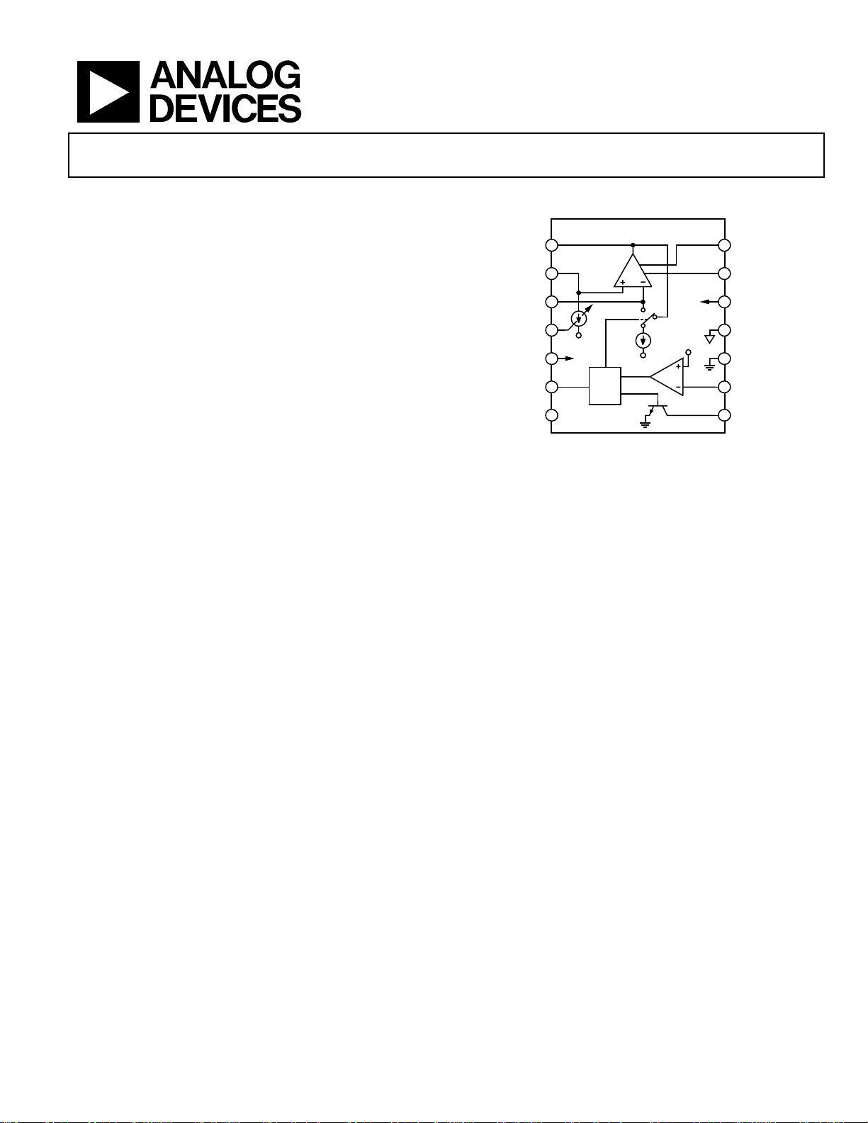
FUNCTIONAL BLOCK DIAGRAM
V
1
OUT
+IN
–IN
BIPOLAR
OFFSET
CURRENT
–V
ONE
SHOT
APACITOR
NC
2
3
4
–V
S
5
S
OUT
FREQ
6
7
NC = NO CONNECT
OP
AMP
ONE
SHOT
IN
OUT
–V
INPUT
OFFSET
TRIM
S1
1mA
–0.6V
S
COMP
Figure 1.
The AD650JN and AD650KN are offered in plastic 14-lead DIP
packages. The AD650JP is available in a 20-lead plastic leaded
chip carrier (PLCC). Both plastic packaged versions of the
AD650 are specified for the commercial temperature range
(0°C to 70°C). For industrial temperature range (−25°C to
+85°C) applications, the AD650AD and AD650BD are offered
in ceramic packages. The AD650SD is specified for the full
−55°C to +125°C extended temperature range.
PRODUCT HIGHLIGHTS
1. Can operate at full-scale output frequencies up to 1 MHz
(in addition to having very high linearity).
2. Can be configured to accommodate bipolar, unipolar, or
differential input voltages, or unipolar input currents.
3. TTL or CMOS compatibility is achieved by using an open
collector frequency output. The pull-up resistor can be
connected to voltages up to 30 V.
4. The same components used for V/F conversion can also be
used for F/V conversion by adding a simple logic biasing
network and reconfiguring the AD650.
5. Separate analog and digital grounds prevent ground loops
in real-world applications.
6. Available in versions compliant with MIL-STD-883.
AD650
OFFSET
14
NULL
OFFSET
13
NULL
+V
12
S
ANALOG
11
GND
DIGITAL
10
GND
COMPARATOR
9
INPUT
F
8
OUTPUT
00797-001
Rev. D
Information furnished by Analog Devices is believed to be accurate and reliable. However, no
responsibility is assumed by Anal og Devices for its use, nor for any infringements of patents or ot her
rights of third parties that may result from its use. Specifications subject to change without notice. No
license is granted by implication or otherwise under any patent or patent rights of Analog Devices.
Trademarks and registered trademarks are the property of their respective owners.
One Technology Way, P.O. Box 9106, Norwood, MA 02062-9106, U.S.A.
Tel: 781.329.4700 www.analog.com
Fax: 781.461.3113 ©2006 Analog Devices, Inc. All rights reserved.
Page 2

AD650
TABLE OF CONTENTS
Features.............................................................................................. 1
F/V Conversion .......................................................................... 10
Functional Block Diagram .............................................................. 1
Product Description......................................................................... 1
Product Highlights ........................................................................... 1
Revision History ............................................................................... 2
Specifications..................................................................................... 3
Absolute Maximum Ratings............................................................ 5
ESD Caution.................................................................................. 5
Pin Configurations and Function Descriptions ........................... 6
Circuit Operation ............................................................................. 7
Unipolar Configuration............................................................... 7
Component Selection................................................................... 8
Bipolar V/F.................................................................................. 10
Unipolar V/F, Negative Input Voltage ..................................... 10
REVISION HISTORY
High Frequency Operation....................................................... 10
Decoupling and Grounding...................................................... 12
Temperature Coefficients .......................................................... 12
Nonlinearity Specification ........................................................ 13
PSRR............................................................................................. 14
Other Circuit Considerations................................................... 14
Applications..................................................................................... 16
Differential Voltage-to-Frequency Conversion...................... 16
Autozero Circuit......................................................................... 16
Phase-Locked Loop F/V Conversion ...................................... 17
Outline Dimensions....................................................................... 19
Ordering Guide .......................................................................... 20
3/06—Rev. C to Rev. D
Updated Format..................................................................Universal
Changes to Product Highlights....................................................... 1
Changes to Table 1............................................................................ 3
Added Pin Function Descriptions Table ...................................... 6
Updated Outline Dimensions....................................................... 18
Changes to Ordering Guide.......................................................... 19
Rev. D | Page 2 of 20
Page 3

AD650
SPECIFICATIONS
T = 25°C, VS = ±15 V, unless otherwise noted.
Table 1.
AD650J/AD650A AD650K/AD650B AD650S
Model Min Typ Max Min Typ Max Min Typ Max Units
DYNAMIC PERFORMANCE
Full-Scale Frequency Range 1 1 1 MHz
Nonlinearity
f
f
f
f
Full-Scale Calibration Error
100 kHz ± 5 ± 5 ± 5 %
1 MHz ± 10 ± 10 ± 10 %
vs. Supply
vs. Temperature
BIPOLAR OFFSET CURRENT
Activated by 1.24 kΩ Between
Pin 4 and Pin 5
DYNAMIC RESPONSE
Maximum Settling Time for
Full-Scale Step Input
Overload Recovery Time
Step Input
ANALOG INPUT AMPLIFIER
(V/F CONVERSION)
Current Input Range (Figure 4) 0 +0.6 0 +0.6 0 +0.6 mA
Voltage Input Range (Figure 12) −10 0 −10 0 −10 0 V
Differen tial Impedance 2 MΩ||10 pF 2 MΩ||10 pF 2 MΩ||10 pF
Common-Mode Impedance 1000 MΩ||10 pF 1000 MΩ||10 pF 1000 MΩ||10 pF
Input Bias Current
Noninverting Input 40 100 40 100 40 100 nA
Inverting Input ±8 ±20 ±8 ±20 ±8 ±20 nA
Input Offset Voltage
(Trimmable to Zero) ±4 ±4 ±4 mV
vs. Temperature (T
Safe Input Voltage ±VS ±VS ±VS V
COMPARATOR (F/V CONVERSION)
Logic 0 Level −VS −1 −VS −1 −VS −1 V
Logic 1 Level 0 +VS 0 +VS 0 +VS V
Pulse Width Range4 0.1 (0.3 × tOS) 0.1 (0.3 × tOS) 0.1 (0.3 × tOS) µs
Input Impedance 250 250 250 kΩ
OPEN COLLECTOR OUTPUT
(V/F CONVERSION)
Output Voltage in Logic 0
I
Output Leakage Current in Logic 1 100 100 100 nA
Voltage Range5 0 36 0 36 0 36 V
1
= 10 kHz 0.002 0.005 0.002 0.005 0.002 0.005 %
MAX
= 100 kHz 0.005 0.02 0.005 0.02 0.005 0.02 %
MAX
= 500 kHz 0.02 0.05 0.02 0.05 0.02 0.05 %
MAX
= 1 MHz 0.1 0.05 0.1 0.05 0.1 %
MAX
3
2
% of
−0.015 +0.015 −0.015 +0.015 −0.015 +0.015
FSR/V
A, B, and S Grades
at 10 kHz ±75 ±75 ±75 ppm/°C
at 100 kHz ±150 ±150 ±200 ppm/°C
J and K Grades
at 10 kHz ±75 ±75 ppm/°C
at 100 kHz ±150 ±150 ppm/°C
0.45 0.5 0.55 0.45 0.5 0.55 0.45 0.5 0.55 mA
1 pulse of new frequency plus 1 s 1 pulse of new frequency plus 1 s 1 pulse of new frequency plus 1 s
1 pulse of new frequency plus 1 s 1 pulse of new frequency plus 1 s 1 pulse of new frequency plus 1 s
to T
MIN
) ±30 ±30 ±30 µV/°C
MAX
≤ 8 mA, T
SINK
MIN
to T
0.4 0.4 0.4 V
MAX
Rev. D | Page 3 of 20
Page 4

AD650
AD650J/AD650A AD650K/AD650B AD650S
Model Min Typ Max Min Typ Max Min Typ Max Units
AMPLIFIER OUTPUT (F/V CONVERSION)
Voltage Range
(1500 Ω Min Load Resistance)
Source Current
(750 Ω Max Load Resistance)
Capacitive Load
(Without Oscillation)
POWER SUPPLY
Voltage, Rated Performance ±9 ±18 ±9 ±18 ±9 ±18 V
Quiescent Current 8 8 8 mA
TEMPERATURE RANGE
Rated Performance
N Package 0 +70 0 +70 °C
D Package −25 +85 −25 +85 −55 +125 °C
1
Nonlinearity is defined as deviation from a straight line from zero to full scale, expressed as a fraction of full scale.
2
Full-scale calibration error adjustable to zero.
3
Measured at full-scale output frequency of 100 kHz.
4
Refer to F/V conversion section of the text.
5
Referred to digital ground.
Specifications shown in boldface are tested on all production units at final electrical test. Results from those tests are used to calculate outgoing quality levels. All min
and max specifications are guaranteed, although only those shown in boldface are tested on all production units.
0 10 0 10 0 10 V
10 10 10 mA
100 100 100 pF
Rev. D | Page 4 of 20
Page 5

AD650
ABSOLUTE MAXIMUM RATINGS
Parameter Rating
Total Supply Voltage 36 V
Storage Temperature Range −55°C to +150°C
Differential Input Voltage ±10 V
Maximum Input Voltage ±VS
Open Collector Output Voltage
Above Digital GND
Current 50 mA
Amplifier Short Circuit to Ground Indefinite
Comparator Input Voltage ±VS
36 V
ESD CAUTION
ESD (electrostatic discharge) sensitive device. Electrostatic charges as high as 4000 V readily accumulate on
the human body and test equipment and can discharge without detection. Although this product features
proprietary ESD protection circuitry, permanent damage may occur on devices subjected to high energy
electrostatic discharges. Therefore, proper ESD precautions are recommended to avoid performance
degradation or loss of functionality.
Stresses above those listed under Absolute Maximum Ratings
may cause permanent damage to the device. This is a stress
rating only; functional operation of the device at these or any
other conditions above those indicated in the operational
section of this specification is not implied. Exposure to absolute
maximum rating conditions for extended periods may affect
device reliability.
Rev. D | Page 5 of 20
Page 6
AD650
PIN CONFIGURATIONS AND FUNCTION DESCRIPTIONS
1
V
OUT
2
+IN
–IN
3
BIBOLAR OFF SET
CURRENT
–V
ONE SHOT
CAPACITOR
AD650
TOP VIEW
4
(Not to Scale)
5
S
6
7
NC
NC = NO CONNECT
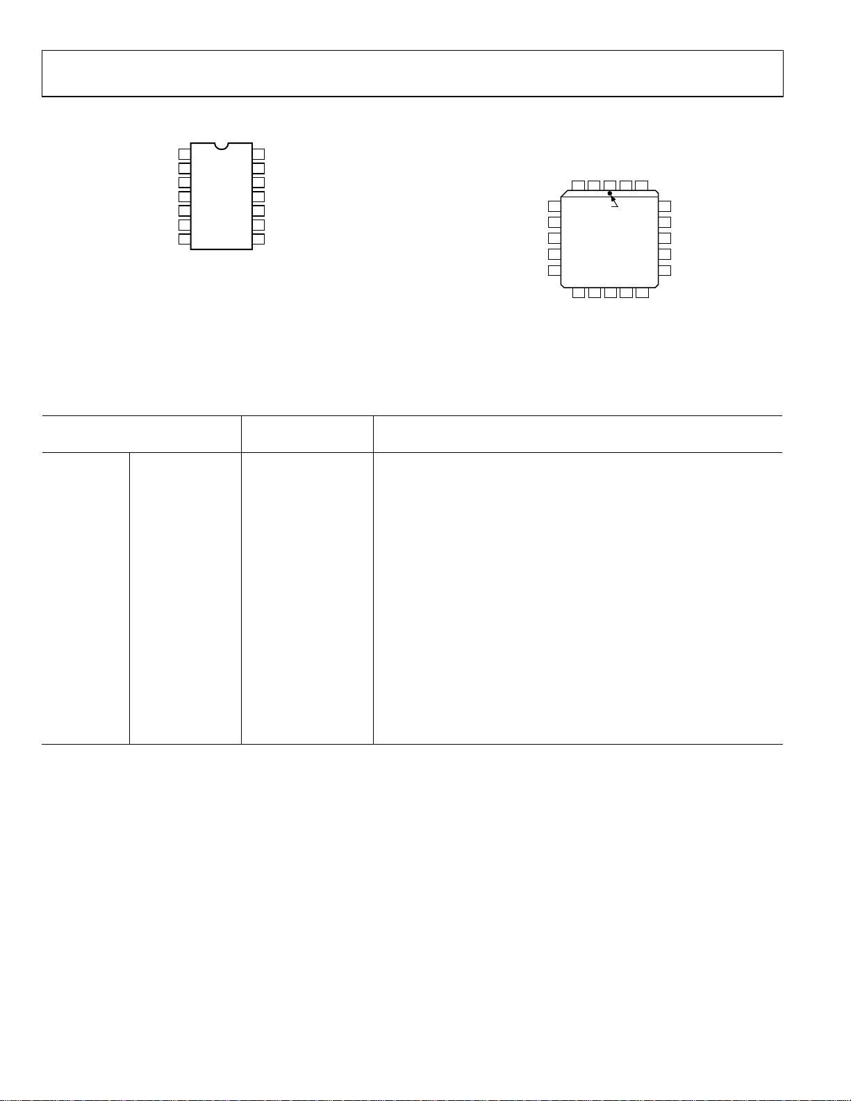
Figure 2. D-14, N-14 Pin Configurations
Table 2. Pin Function Descriptions
Pin No.
D-14, N-14 P-20A Mnemonic Description
1 2 V
2 3 +IN Positive Analog Input.
3 4 –IN Negative Analog Input.
4 6
5 8 –VS Negative Power Supply Input.
6 9
7 1, 5, 7, 10, 11, 15, 17 NC No Connect.
8 12 F
9 13 COMPARATOR INPUT
10 14 DIGITAL GND Digital Ground.
11 16 ANALOG GND Analog Ground.
12 18 +VS Positive Power Supply Input.
13, 14 19, 20 OFFSET NULL
OFFSET NULL
14
13
OFFSET NULL
12
+V
S
ANALOG GND
11
DIGITAL GND
10
COMPARATOR
9
INPUT
8
F
OUTPUT
00797-010
NC = NO CONNECT
OUT
Output of Operational Amplifier. The operational amplifier, along with C
is used in the integrate stage of the V to F conversion.
BIPOLAR OFFSET
CURRENT
ONE-SHOT
CAPACITOR
Frequency Output from AD650.
OUTPUT
On-Chip Current Source. This can be used in conjunction with an external
resistor to remove the operational amplifier’s offset.
The Capacitor, C
OS
for the one shot.
Input to Comparator. When the input voltage reaches −0.6 V, the one shot is
triggered.
Offset Null Pins. Using an external potentiometer, the offset of the
operational amplifier can be removed.
BIPOLAR O FFSET
CURRENT
, is Connected to This Pin. COS determines the time period
OUT
+IN
V
NC
OFFSET
NULL
OFFSET
NC
NULL
18
17
16
15
14
INPUT
OUTPUT
F
COMPARATOR
–V
–IN
NC
NC
4
5
6
7
8
S
1201923
PIN 1
INDENTFIER
AD650
TOP VIEW
(Not to scale)
91011 12 13
NC
ONE SHOT
CAPACITOR
Figure 3. P-20A Pin Configuration
+V
S
NC
ANALOG GND
NC
DIGITAL GND
00797-011
,
INT
Rev. D | Page 6 of 20
Page 7

AD650
+
–
+
–
–
CIRCUIT OPERATION
C
I
IN
–V
1mA
–V
OS
FREQUENCY
OUTPUT
ONE
SHOT
t
OS
IN
1mA
S
00797-005
IN
1mA
S
00797-006
T
1
INT
t
00797-004
t
0797-007
UNIPOLAR CONFIGURATION
The AD650 is a charge balance voltage-to-frequency converter.
In the connection diagram shown in
diagram of
Figure 5, the input signal is converted into an
equivalent current by the input resistance R
exactly balanced by an internal feedback current delivered in
short, timed bursts from the switched 1 mA internal current
source. These bursts of current can be thought of as precisely
defined packets of charge. The required number of charge
packets, each producing one pulse of the output transistor,
depends upon the amplitude of the input signal. Because the
number of charge packets delivered per unit time is dependent
on the input signal amplitude, a linear voltage-to-frequency
transformation is accomplished. The frequency output is
furnished via an open collector transistor.
A more rigorous analysis demonstrates how the charge balance
voltage-to-frequency conversion takes place.
A block diagram of the device arranged as a V-to-F converter is
shown in
Figure 5. The unit is comprised of an input integrator,
a current source and steering switch, a comparator, and a one
shot. When the output of the one shot is low, the current
steering switch S
diverts all the current to the output of the op
1
amp; this is called the integration period. When the one shot
has been triggered and its output is high, the switch S
all the current to the summing junction of the op amp; this is
called the reset period. The two different states are shown in
Figure 6 and Figure 7 along with the various branch currents. It
should be noted that the output current from the op amp is the
same for either state, thus minimizing transients.
S
OUT
AMP
ONE
SHOT
AD650
OP
IN
OUT
C
INT
1 14
2
3
4
–V
5
FREQ
6
C
OS
7
–15V
R
IN
V
IN
R3 R1
0.1µF
Figure 4. Connection Diagram for V/F Conversion, Positive Input Voltage
Figure 4, or the block
IN
INPUT
OFFSET
TRIM
S1
1mA
–0.6V
–V
S
COMP
. This current is
diverts
1
20kΩ
13
12
11
10
9
8
0.1µF
DIGITAL
GROUND
1µF
250kΩ
R2
+15V
ANALOG
GROUND
V
F
LOGIC
OUT
C
INT
COMPARATOR
–0.6V
S1
1mA ± 20%
–V
S
+
V
–
I
IN
R
IN
IN
INTEGRATOR
AD650
Figure 5. Block Diagram
C
INT
I
IN
R
V
IN
IN
1mA
1mA – I
S1
Figure 6. Reset Mode
C
INT
I
IN
R
V
IN
IN
1mA – I
S1
Figure 7. Integrate Mode
RESET INTEGRATE
VOLTS
0797-003
0.6
ΔV
t
OS
Figure 8. Voltage Across C
Rev. D | Page 7 of 20
Page 8

AD650
t
×
−
MAX
The positive input voltage develops a current (IIN = VIN/RIN) that
charges the integrator capacitor C
C
, the output voltage of the integrator ramps downward
INT
towards ground. When the integrator output voltage (Pin 1)
crosses the comparator threshold (–0.6 V) the comparator
triggers the one shot, whose time period, t
the one-shot capacitor C
.
OS
Specifically, the one-shot time period is
Ct (1)
OSOS
The reset period is initiated as soon as the integrator output
voltage crosses the comparator threshold, and the integrator
ramps upward by an amount
dV
tV −=×=Δ mA1
OS
OS
(
C
dt
INT
After the reset period has ended, the device starts another
integration period, as shown in
downward again. The amount of time required to reach the
comparator threshold is given as
t
OS
()
mA1
C
Δ
V
INT
=
= 1
1
T
dV
dt
I
N
C
INT
The output frequency is now given as
f
OUT
15.0
Note that C
1
=
Tt
+
OS
F
Hz
×
A
OS
, the integration capacitor, has no effect on the
INT
I
IN
=
t
×
1
OS
RV
/
104.4
×+
transfer relation, but merely determines the amplitude of the
sawtooth signal out of the integrator.
One-Shot Timing
A key part of the preceding analysis is the one-shot time period
given in Equation 1. This time period can be broken down into
approximately 300 ns of propagation delay and a second time
segment dependent linearly on timing capacitor C
one shot is triggered, a voltage switch that holds Pin 6 at analog
ground is opened, allowing that voltage to change. An internal
0.5 mA current source connected to Pin 6 then draws its
current out of C
, causing the voltage at Pin 6 to decrease
OS
linearly. At approximately –3.4 V, the one shot resets itself,
thereby ending the timed period and starting the V/F
conversion cycle over again. The total one-shot time period can
be written mathematically as
CV
Δ
OS
t +
= (5)
OS
I
DISCHARGE
T
substituting actual values quoted in Equation 5,
. As charge builds up on
INT
is determined by
OS
73 −
sec100.3F/sec108.6
×+××=
)
I
(2)
IN
Figure 8, and starts ramping
I
−
IN
=
mA1
mA1
⎛
⎜
t
OS
⎜
⎝
⎞
⎟
(3)
−=
⎟
I
IN
⎠
(4)
ININ
−
11
FC
. When the
OS
DELAYGATE
Rev. D | Page 8 of 20
V4.3
C
t
=
OS
OS
−
A105.0
×−
93−
sec10300
×+
(6)
This simplifies into the timed period equation (see Equation 1).
COMPONENT SELECTION
Only four component values must be selected by the user. These
are input resistance R
and integration capacitor C
input voltage and full-scale frequency, while the last two are
determined by other circuit considerations.
Of the four components to be selected, R2 is the easiest to
define. As a pull-up resistor, it should be chosen to limit the
current through the output transistor to 8 mA if a TTL
maximum V
of 0.4 V is desired. For example, if a 5 V logic
OL
supply is used, R2 should be no smaller than 5 V/8 mA or
625 . A larger value can be used if desired.
R
and COS are the only two parameters available to set the full-
IN
scale frequency to accommodate the given signal range. The swing
variable that is affected by the choice of R
The selection guides of
graphically. In general, larger values of C
input currents (higher values of R
Figure 10, the implications of four different choices of RIN are
shown. Although the selection guide is set up for a unipolar
configuration with a 0 V to 10 V input signal range, the results
can be extended to other configurations and input signal ranges.
For a full-scale frequency of 100 kHz (corresponding to 10 V
input), among the available choices R
gives the lowest nonlinearity, 0.0038%. In addition, the highest
frequency that gives the 20 ppm minimum nonlinearity is
approximately 33 kHz (40.2 k and 1000 pF).
For input signal spans other than 10 V, the input resistance
must be scaled proportionately. For example, if 100 k is called
out for a 0 V to 10 V span, 10 kΩ would be used with a 0 V to 1 V
span, or 200 k with a ±10 V bipolar connection.
The last component to be selected is the integration capacitor
C
. In almost all cases, the best value for C
INT
using the equation
C
= (7)
INT
When the proper value for C
architecture of the AD650 provides continuous integration
of the input signal, therefore, large amounts of noise and
interference can be rejected. If the output frequency is
measured by counting pulses during a constant gate period,
the integration provides infinite normal-mode rejection for
frequencies corresponding to the gate period and its harmonics.
However, if the integrator stage becomes saturated by an
excessively large noise pulse, then the continuous integration of
the signal is interrupted, allowing the noise to appear at the output.
, timing capacitor COS, logic resistor R2,
IN
. The first two determine the
INT
and COS is nonlinearity.
IN
Figure 9 and Figure 10 show this quite
and lower full-scale
OS
) provide better linearity. In
IN
= 20 kΩ and COS = 620 pF
IN
INT
4
−
F
sec/10
(
f
minimumpF1000
is used, the charge balance
INT
)
can be calculated
Page 9

AD650
If the approximate amount of noise that appears on C
(V
), then the value of C
NOISE
can be checked using the following
INT
inequality:
C
INT
OS
>
V3
−−+
(8)
VV
NOISES
−
3
At
101
××
For example, consider an application calling for a maximum
frequency of 75 kHz, a 0 V to 1 V signal range, and supply
voltages of only ±9 V. The component selection guide of
is used to select 2.0 k for R
and 1000 pF for COS. This results
IN
in a one-shot time period of approximately 7 s. Substituting
75 kHz into Equation 7 yields a value of 1300 pF for C
the input signal is near zero, 1 mA flows through the integration
capacitor to the switched current sink during the reset phase,
causing the voltage across C
to increase by approximately 5.5 V.
INT
Because the integrator output stage requires approximately 3 V
headroom for proper operation, only 0.5 V margin remains for
integrating extraneous noise on the signal line. A negative noise
pulse at this time could saturate the integrator, causing an error
in signal integration. Increasing C
to 1500 pF or 2000 pF
INT
provides much more noise margin, thereby eliminating this
potential trouble spot.
is known
INT
Figure 9
. When
INT
100kHz
FREQUENCY FULL-SCALE
1MHz
10kHz
1000
100
50 100 1000
COS (pF)
Figure 9. Full-Scale Frequency vs. COS
INPUT
RESISTOR
16.9k
20k
40.2k
100k
INPUT
RESISTOR
16.9k
20k
40.2k
100k
00797-008
TYPICAL NO NLINEARIT Y (ppm)
20
50 100 1000
ONE SHOT CAPACITOR
C
(pF)
OS
Figure 10. Typical Nonlinearity vs. C
OS
00797-009
Rev. D | Page 9 of 20
Page 10

AD650
V
BIPOLAR V/F
Figure 11 shows how the internal bipolar current sink is used to
provide a half-scale offset for a ±5 V signal range, while providing
a 100 kHz maximum output frequency. The nominally 0.5 mA
(±10%) offset current sink is enabled when a 1.24 k resistor is
connected between Pin 4 and Pin 5. Thus, with the grounded
10 k nominal resistance shown, a −5 V offset is developed at
Pin 2. Because Pin 3 must also be at −5 V, the current through R
is 10 V/40 k = +0.25 mA at V
= +5 V, and 0 mA at VIN = –5 V.
IN
Components are selected using the same guidelines outlined for
t
he unipolar configuration with one alteration. The voltage
across the total signal range must be equated to the maximum
input voltage in the unipolar configuration. In other words, the
value of the input resistor R
is determined by the input voltage
IN
span, not the maximum input voltage. A diode from Pin 1 to
ground is also recommended. This is further discussed in the
Other Circuit Considerations section.
As in the unipolar circuit, R
and COS must have low temperature
IN
coefficients to minimize the overall gain drift. The 1.24 k
resistor used to activate the 0.5 mA offset current should also
have a low temperature coefficient. The bipolar offset current
has a temperature coefficient of approximately −200 ppm/°C.
UNIPOLAR V/F, NEGATIVE INPUT VOLTAGE
Figure 12 shows the connection diagram for V/F conversion of
negative input voltages. In this configuration, full-scale output
frequency occurs at negative full-scale input, and zero output
frequency corresponds with zero input voltage.
A very high impedance signal source can be used because it only
d
rives the noninverting integrator input. Typical input impedance
at this terminal is 1 G or higher. For V/F conversion of positive
input signals using the connection diagram of
enerator must be able to source the integration current
signal g
to drive the AD650. For the negative V/F conversion circuit of
Figure 12, the integration current is drawn from ground
t
hrough R1 and R3, and the active input is high impedance.
Figure 4, the
IN
Circuit operation for negative input voltages is very similar to
ositive input unipolar conversion described in the
p
onfiguration section. For best operating results use Equation 7
C
an
d Equation 8 in the Component Selection section.
Unipo lar
F/V CONVERSION
The AD650 also makes a very linear frequency-to-voltage
converter. Figure 13 shows the connection diagram for F/V
co
nversion with TTL input logic levels. Each time the input
signal crosses the comparator threshold going negative, the one
shot is activated and switches 1 mA into the integrator input for
a measured time period (determined by C
). As the frequency
OS
increases, the amount of charge injected into the integration
capacitor increases proportionately. The voltage across the
integration capacitor is stabilized when the leakage current
through R1 and R3 equals the average current being switched
into the integrator. The net result of these two effects is an
average output voltage that is proportional to the input
frequency. Optimum performance can be obtained by selecting
components using the same guidelines and equations listed in
the
Bipolar V/F section.
For a more complete description of this application, refer to
log Devices’ Application Note AN-279.
Ana
HIGH FREQUENCY OPERATION
Proper RF techniques must be observed when operating the
AD650 at or near its maximum frequency of 1 MHz. Lead
lengths must be kept as short as possible, especially on the one
shot and integration capacitors, and at the integrator summing
junction. In addition, at maximum output frequencies above
500 kHz, a 3.6 k pull-down resistor from Pin 1 to −V
required (see Figure 14). The additional current drawn through
t
he pulldown resistor reduces the op amp’s output impedance
and improves its transient response.
is
S
S
OUT
OP
AMP
ONE
SHOT
AD650
–V
IN
OUT
INPUT
OFFSET
TRIM
S1
1mA
–0.6V
S
COMP
20kΩ
13
12
11
10
9
8
0.1µF
DIGITAL
GND
250kΩ
1µF
ANALOG
GND
1kΩ
+15V
+5V
F
OUT
00797-012
C
INT
1000pF
R1
5kΩ
V
IN
±5
–15V
R3
37.4kΩ
1.24kΩ
0.1µF
C
330pF
OS
1 14
2
10kΩ
3
4
–V
5
FREQ
6
7
Figure 11. Connections for ±5 V Bipolar V/F with 0 kHz to 100 kHz TTL Output
Rev. D | Page 10 of 20
Page 11

AD650
V
R3
C
INT
R1
AD650
–V
–15V
1 14
OP
–V
FREQ
S
OUT
AMP
ONE
SHOT
IN
OUT
–V
IN
0.1µF
C
OS
2
3
4
5
6
7
INPUT
OFFSET
TRIM
S1
1mA
–0.6V
S
COMP
20kΩ
13
12
250kΩ
+15V
0.1µF
11
10
DIGITAL
9
GND
8
1µF
ANALOG
GND
R2
+V
F
LOGIC
OUT
00797-013
Figure 12. Connection Diagram for V/F Conversion, Negative Input Voltage
OUT
–15V
R3
R1
1 14
C
INT
2
3
4
–V
0.1µF
C
OS
5
6
7
FREQ
Figure 13. Connection Diagram for F/V Conversion
S
OUT
OP
AMP
ONE
SHOT
AD650
–V
IN
OUT
INPUT
OFFSET
TRIM
S1
1mA
–0.6V
S
COMP
20kΩ
13
250kΩ
12
+15V
0.1µF
11
10
9
1N914
8
500Ω
2kΩ
ANALOG
GND
560pF
500Ω
F
+5V
IN
00797-014
S
OUT
OP
AMP
ONE
SHOT
AD650
–V
IN
OUT
OFFSET
INPUT
OFFSET
TRIM
S1
1mA
–0.6V
S
COMP
ADJUST
20kΩ
13
250kΩ
12
+15V
0.1µF
11
10
1µF
9
8
510Ω
ANALOG
GND PLANE
DIGITAL
GND
+5V
F
OUT
0MHz TO 1MHz
00797-015
V
0V TO 10V
IN
GAIN
ADJUST
5kΩ
14.3kΩ
–15V
1000pF
1 14
2
3
3.6kΩ
4
–V
5
0.1µF
51pF
6
7
FREQ
Figure 14. 1 MHz V/F Connection Diagram
Rev. D | Page 11 of 20
Page 12

AD650
DECOUPLING AND GROUNDING
It is effective engineering practice to use bypass capacitors on
the supply-voltage pins and to insert small-valued resistors
(10 to 100 ) in the supply lines to provide a measure of
decoupling between the various circuits in a system. Ceramic
capacitors of 0.1 F to 1.0 F should be applied between the
supply-voltage pins and analog signal ground for proper
bypassing on the AD650.
In addition, a larger board level decoupling capacitor of 1 F to
10 F should be located relatively close to the AD650 on each
power supply line. Such precautions are imperative in high
resolution, data acquisition applications where users expect to
exploit the full linearity and dynamic range of the AD650.
Although some types of circuits can operate satisfactorily with
power supply decoupling at only one location on each circuit
board, such practice is strongly discouraged in high accuracy
analog design.
Separate digital and analog grounds are provided on the
AD650. The emitter of the open collector frequency output
transistor is the only node returned to the digital ground. All
other signals are referred to analog ground. The purpose of the
two separate grounds is to allow isolation between the high
precision analog signals and the digital section of the circuitry.
As much as several hundred millivolts of noise can be tolerated
on the digital ground without affecting the accuracy of the
VFC. Such ground noise is inevitable when switching the large
currents associated with the frequency output signal.
At 1 MHz full scale, it is necessary to use a pull-up resistor of
about 500 in order to get the rise time fast enough to provide
well defined output pulses. This means that from a 5 V logic
supply, for example, the open collector output draws 10 mA.
This much current being switched causes ringing on long
ground runs due to the self-inductance of the wires. For
instance, 20 gauge wire has an inductance of about 20 nH per
inch; a current of 10 mA being switched in 50 ns at the end of
12 inches of 20 gauge wire produces a voltage spike of 50 mV.
The separate digital ground of the AD650 easily handles these
types of switching transients.
A problem remains from interference caused by radiation of
electromagnetic energy from these fast transients. Typically, a
voltage spike is produced by inductive switching transients;
these spikes can capacitively couple into other sections of the
circuit. Another problem is ringing of ground lines and power
supply lines due to the distributed capacitance and inductance
of the wires. Such ringing can also couple interference into
sensitive analog circuits. The best solution to these problems is
proper bypassing of the logic supply at the AD650 package. A
1 F to 10 F tantalum capacitor should be connected directly
to the supply side of the pull-up resistor and to the digital
ground (Pin 10). The pull-up resistor should be connected
directly to the frequency output (Pin 8). The lead lengths on the
bypass capacitor and the pull-up resistor should be as short as
possible. The capacitor supplies (or absorbs) the current
transients, and large ac signals flows in a physically small loop
through the capacitor, pull-up resistor, and frequency output
transistor. It is important that the loop be physically small for
two reasons: first, there is less self-inductance if the wires are
short, and second, the loop does not radiate RFI efficiently.
The digital ground (Pin 10) should be separately connected to
the power supply ground. Note that the leads to the digital
power supply are only carrying dc current and cannot radiate
RFI. There can also be a dc ground drop due to the difference in
currents returned on the analog and digital grounds. This does
not cause any problem. In fact, the AD650 tolerates as much as
0.25 V dc potential difference between the analog and digital
grounds. These features greatly ease power distribution and
ground management in large systems. Proper technique for
grounding requires separate digital and analog ground returns
to the power supply. Also, the signal ground must be referred
directly to analog ground (Pin 11) at the package. All of the
signal grounds should be tied directly to Pin 11, especially the
one-shot capacitor. More information on proper grounding and
reduction of interference can be found in “Noise Reduction
Techniques in Electronic Systems, 2
nd
edition” by Henry W. Ott,
(John Wiley & Sons, Inc., 1988).
TEMPERATURE COEFFICIENTS
The drift specifications of the AD650 do not include
temperature effects of any of the supporting resistors or
capacitors. The drift of the input resistors R1 and R3 and the
timing capacitor C
stability. In the application of
resistor used with a 100 ppm/°C capacitor can result in a
maximum overall circuit gain drift of:
150 ppm/°C (AD650A) + 100 ppm/°C (C
+ 10 ppm/°C (R
In bipolar configuration, the drift of the 1.24 k resistor used to
activate the internal bipolar offset current source directly affects
the value of this current. This resistor should be matched to the
resistor connected to the op amp noninverting input, Pin 2 (see
Figure 11). That is, the temperature coefficients of these two
resistors should be equal. If this is the case, then the effects of the
temperature coefficients of the resistors cancel each other, and the
drift of the offset voltage developed at the op amp noninverting
input is solely determined by the AD650. Under these conditions,
the TC of the bipolar offset voltage is typically −200 ppm/°C and
is a maximum of −300 ppm/°C. The offset voltage always
decreases in magnitude as temperature is increased.
directly affect the overall temperature
OS
Figure 5, a 10 ppm/°C input
)
OS
) = 260 ppm/°C
IN
Rev. D | Page 12 of 20
Page 13

AD650
Other circuit components do not directly influence the accuracy
of the VFC over temperature changes as long as their actual
values are not as different from the nominal value as to preclude
operation. This includes the integration capacitor C
in the capacitance value of C
simply results in a different rate of
INT
. A change
INT
voltage change across the capacitor. During the integration phase
(see
Figure 8), the rate of voltage change across C
has the
INT
opposite effect that it does during the reset phase. The result is
that the conversion accuracy is unchanged by either drift or
tolerance of C
. The net effect of a change in the integrator
INT
capacitor is simply to change the peak-to-peak amplitude of the
sawtooth waveform at the output of the integrator.
The gain temperature coefficient of the AD650 is not a constant
value. Rather, the gain TC is a function of both the full-scale
frequency and the ambient temperature. At a low full-scale
frequency, the gain TC is determined primarily by the stability of
the internal reference (a buried Zener reference). This low speed
gain TC can be quite effective; at 10 kHz full scale, the gain TC near
25°C is typically 0 ± 50 ppm/°C. Although the gain TC changes
with ambient temperature (tending to be more positive at higher
temperatures), the drift remains within a ±75 ppm/°C window over
the entire military temperature range. At full-scale frequencies
higher than 10 kHz, dynamic errors become much more important
than the static drift of the dc reference. At a full-scale frequency
of 100 kHz and above, these timing errors dominate the gain
TC. For example, at 100 kHz full-scale frequency (R
C
= 330 pF) the gain TC near room temperature is typically
OS
= 40 k and
IN
−80 ±50 ppm/°C, but at an ambient temperature near 125°C, the
gain TC tends to be more positive and is typically 15 ±50 ppm/°C.
This information is presented in a graphical form in
Figure 15.
The gain TC always tends to become more positive at higher
temperatures. Therefore, it is possible to adjust the gain TC of
the AD650 by using a one-shot capacitor with an appropriate
TC to cancel the drift of the circuit. For example, consider the
100 kHz full-scale frequency. An average drift of −100 ppm/°C
means that as temperature is increased, the circuit produces a
lower frequency in response to a given input voltage. This means
that the one-shot capacitor must decrease in value as temperature
increases in order to compensate the gain TC of the AD650; that
is, the capacitor must have a TC of −100 ppm/°C. Now consider
the 1 MHz full-scale frequency.
100
–50
0
–100
–200
GAIN TC (ppm/°C)
–300
–400
10kHz
100kHz
1MHz
Figure 15. Gain TC vs. Temperature
TEMPERATURE (° C)
–250 255075
100 125
00797-016
Rev. D | Page 13 of 20
It is not possible to achieve much improvement in performance
unless the expected ambient temperature range is known. For
example, in a constant low temperature application such as
gathering data in an Arctic climate (approximately −20°C), a
C
with a drift of −310 ppm/°C is called for in order to compensate
OS
the gain drift of the AD650. However, if that circuit should see
an ambient temperature of 75°C, then the C
capacitor would
OS
change the gain TC from approximately 0 ppm to 310 ppm/°C.
The temperature effects of these components are the same when
the AD650 is configured for negative or bipolar input voltages,
and for F/V conversion as well.
NONLINEARITY SPECIFICATION
The linearity error of the AD650 is specified by the endpoint
method. That is, the error is expressed in terms of the deviation
from the ideal voltage to frequency transfer relation after
calibrating the converter at full scale and zero. The nonlinearity
varies with the choice of one-shot capacitor and input resistor
(see
Figure 10). Verification of the linearity specification
requires the availability of a switchable voltage source (or a
DAC) having a linearity error below 20 ppm, and the use of
very long measurement intervals to minimize count
uncertainties. Every AD650 is automatically tested for linearity,
and it is not usually necessary to perform this verification,
which is both tedious and time consuming. If it is required to
perform a nonlinearity test either as part of an incoming quality
screening or as a final product evaluation, an automated benchtop tester proves useful. Such a system based on Analog
Devices’ LTS-2010 is described in “V-F Converters Demand
Accurate Linearity Testing,” by L. DeVito, (Electronic Design,
March 4, 1982).
The voltage-to-frequency transfer relation is shown in
and
Figure 17 with the nonlinearity exaggerated for clarity. The
first step in determining nonlinearity is to connect the endpoints of
the operating range (typically at 10 mV and 10 V) with a straight
line. This straight line is then the ideal relationship that is desired
from the circuit. The second step is to find the difference between
this line and the actual response of the circuit at a few points
between the endpoints—typically ten intermediate points
suffices. The difference between the actual and the ideal
response is a frequency error measured in hertz. Finally, these
frequency errors are normalized to the full-scale frequency and
expressed either as parts per million of full scale (ppm) or parts
per hundred of full scale (%). For example, on a 100 kHz full
scale, if the maximum frequency error is 5 Hz, the nonlinearity
is specified as 50 ppm or 0.005%. Typically on the 100 kHz
scale, the nonlinearity is positive and the maximum value
occurs at about midscale (
Figure 16). At higher full-scale
frequencies, (500 kHz to 1 MHz), the nonlinearity becomes “S”
shaped and the maximum value can be either positive or negative.
Typically, on the 1 MHz scale (R
= 16.9 k, COS = 51 pF) the
IN
nonlinearity is positive below about 2/3 scale and is negative
above this point. This is shown graphically in
Figure 17.
Figure 16
Page 14

AD650
100k
OUTPUT F REQUENCY (Hz)
100
ACTUAL
50ppm
IDEAL
PSRR
The power supply rejection ratio is a specification of the change
in gain of the AD650 as the power supply voltage is changed.
The PSRR is expressed in units of parts-per-million change of
the gain per percent change of the power supply (ppm/%). For
example, consider a VFC with a 10 V input applied and an
output frequency of exactly 100 kHz when the power supply
potential is ±15 V. Changing the power supply to ±12.5 V is a
5 V change out of 30 V, or 16.7%. If the output frequency changes
to 99.9 kHz, then the gain has changed 0.1% or 1000 ppm. The
PSRR is 1000 ppm divided by 16.7%, which equals 60 ppm/%.
10mV
Figure 16. Exaggerated Nonlinearity at 100 kHz Full Scale
INPUT VOLTAGE
10V
00797-017
The PSRR of the AD650 is a function of the full-scale operating
frequency. At low full-scale frequencies the PSRR is determined
by the stability of the reference circuits in the device and can be
very effective. At higher frequencies, there are dynamic errors
that become more important than the static reference signals,
and consequently the PSRR is not quite as effective. The values
1M
ACTUAL
VOLTAGE TO FREQUENCY
TRANSFER REL ATION
600ppm
600ppm
IDEAL RELATION
of PSRR are typically 0 ± 20 ppm/% at 10 kHz full-scale frequency
(R
= 40 k, COS = 3300 pF). At 100 kHz (RIN = 40 k, COS =
IN
330 pF) the PSRR is typically +80 ± 40 ppm/%, and at 1 MHz
(R
= 16.9 k, COS = 51 pF) the PSRR is +350 ± 50 ppm/%.
IN
This information is summarized graphically in
Figure 18.
OTHER CIRCUIT CONSIDERATIONS
The input amplifier connected to Pin 1, Pin 2, and Pin 3 is not a
OUTPUT FREQUENCY (Hz)
1k
standard operational amplifier. Rather, the design has been
optimized for simplicity and high speed. The single largest
difference between this amplifier and a normal op amp is the lack
10mV
Figure 17. Exaggerated Nonlinearity at 1 MHz Full Scale
INPUT VOLTAGE
10V
00797-018
of an integrator (or level shift) stage. Consequently, the voltage on
the output (Pin 1) must always be more positive than 2 V below the
inputs (Pin 2 and Pin 3). For example, in the F-to-V conversion
mode (
Figure 13) the noninverting input of the op amp (Pin 2)
is grounded, which means that the output (Pin 1) is not able to
go below –2 V. Normal operation of the circuit shown in
Figure 13
never calls for a negative voltage at the output, but users can
1k
imagine an arrangement calling for a bipolar output voltage (for
example, ±10 V) by connecting an extra resistor from Pin 3 to a
positive voltage. However, this does not work.
100
PSRR (ppm/%)
Care should be taken under conditions where a high positive
input voltage exists at or before power up. These situations can
cause a latch up at the integrator output (Pin 1). This is a
10
nondestructive latch and, as such, normal operation can be
restored by cycling the power supply. Latch up can be prevented
by connecting two diodes (for example, 1N914 or 1N4148) as
10k 100k 1M
FULL SCAL E FREQUENCY (Hz )
Figure 18. PSRR vs. Full-Scale Frequency
00797-019
shown in
below Pin 2.
Figure 11, thereby preventing Pin 1 from swinging
Rev. D | Page 14 of 20
Page 15

AD650
A
A second major difference is that the output only sinks 1 mA to
the negative supply. There is no pulldown stage at the output
other than the 1 mA current source used for the V-to-F
conversion. The op amp sources a great deal of current from the
positive supply, and it is internally protected by current limiting.
The output of the op amp can be driven to within 3 V of the
positive supply when it is not sourcing external current. When
sourcing 10 mA the output voltage can be driven to within 6 V
of the positive supply.
A third difference between this op amp and a normal device is
that the inverting input, Pin 3, is bias current compensated and
the noninverting input is not bias-current compensated. The
bias current at the inverting input is nominally zero, but can be
as much as 20 nA in either direction. The noninverting input
typically has a bias current of 40 nA that always flows into the
node (an npn input transistor). Therefore, it is not possible to
match input voltage drops due to bias currents by matching
input resistors.
The bipolar offset current is activated by connecting a 1.24 k
resistor between Pin 4 and the negative supply. The resulting
current delivered to the op amp noninverting input is nominally
0.5 mA and has a tolerance of ±10%. This current is then used
to provide an offset voltage when Pin 2 is tied to ground through
a resistor. The 0.5 mA that appears at Pin 2 is also flowing
through the 1.24 k resistor. An external resistor is used to
activate the bipolar offset current source to provide the lowest
tolerance and temperature drift of the resulting offset voltage.
It is possible to use other values of resistance between Pin 4 and
−V
to obtain a bipolar offset current different from 0.5 mA.
S
Figure 19 shows the relationship between the bipolar offset
current and the value of the resistor used to activate the source.
µ
1000
800
The op amp has provisions for trimming the input offset
voltage. A potentiometer of 20 k is connected from Pin 13 to
Pin 14 and the wiper is connected to the positive supply
through a 250 k resistor. A potential of about 0.6 V is
established across the 250 k resistor, and the 3 A current is
injected into the null pins. It is also possible to null the op amp
offset voltage by using only one of the null pins and by using a
bipolar current either into or out of the null pin. The amount of
current required is very small—typically less than 3 A. This
technique is shown in the
Applications section of this data
sheet; the autozero circuit uses this technique.
600
400
BIPOLAR OFFSET CURRENT
200
500 4000
1000 1500 2000 2500 3000 3500
EXTERNAL RESI STOR
Figure 19. Bipolar Offset Current vs. External Resistor
Ω
00797-020
Rev. D | Page 15 of 20
Page 16

AD650
T
APPLICATIONS
DIFFERENTIAL VOLTAGE-TO-FREQUENCY CONVERSION
The circuit in Figure 20 accepts a true floating differential input
signal. The common-mode input, V
+15 V to −5 V with respect to analog ground. The signal input,
V
, can be ±5 V with respect to the common-mode input. Both
IN
inputs are low impedance; the source that drives the commonmode input must supply the 0.5 mA drawn by the bipolar offset
current source, and the source that drives the signal input must
supply the integration current.
If less common-mode voltage range is required, then a lower
voltage Zener can be used. For example, if a 5 V Zener is used,
the V
input can be in the range +10 V to −5 V. If the Zener is
CM
not used at all, the common-mode range is ±5 V with respect to
analog ground. If no Zener is used, the 10 k pulldown resistor
is not needed and the integrator output (Pin 1) is connected
directly to the comparator input (Pin 9).
AUTOZERO CIRCUIT
In order to exploit the full dynamic range of the AD650 VFC,
very small input voltages need to be converted. For example, a
six decade dynamic range based on a full scale of 10 V requires
accurate measurement of signals down to 10 V. In these
situations, a well-controlled input offset voltage is imperative. A
constant offset voltage does not affect dynamic range but simply
shifts all of the frequency readings by a few hertz. However, if
the offset should change, it is not possible to distinguish
between a small change in a small input voltage and a drift of
the offset voltage. Therefore, the usable dynamic range is less.
The circuit shown in
of the op amp offset voltage. The circuit uses an AD582 sample-
Figure 21 provides automatic adjustment
, can be in the range
CM
and-hold amplifier to control the offset, and the input voltage to
the VFC is switched between ground and the signal to be
measured via an
AD7512DI analog switch. The offset of the
AD650 is adjusted by injecting a current into—or drawing a
current out of—Pin 13. Note that only one of the offset null pins
is used. During the VFC norm mode, the SHA is in the hold
mode and the hold capacitor is very large, 0.1 F, which holds
the AD650 offset constant for a long period of time.
When the circuit is in the autozero mode, the SHA is in sample
mode and behaves like an op amp. The circuit is a variation of
the classical two amplifier servo loop, where the output of the
device under test (DUT)—here the DUT is the AD650 op
amp—is forced to ground by the feedback action of the control
amplifier—the SHA. Because the input of the VFC circuit is
connected to ground during the autozero mode, the input
current that can flow is determined by the offset voltage of the
AD650 op amp. Because the output of the integrator stage is
forced to ground, it is known that the voltage is not changing (it
is equal to ground potential). Therefore, if the output of the
integrator is constant, its input current must be zero, so the
offset voltage has been forced to be zero. Note that the output of
the DUT could have been forced to any convenient voltage
other than ground. All that is required is that the output voltage
be known to be constant. Note also that the effect of the bias
current at the inverting input of the AD650 op amp is also
mulled in this circuit. The 1000 pF capacitor shunting the
200 k resistor is compensation for the two amplifier servo
loop. Two integrators in a loop require a single zero for
compensation. The 3.6 k resistor from Pin 1 of the AD650 to
the negative supply is not part of the autozero circuit, but rather,
it is required for VFC operation at 1 MHz.
10V ZENER 1N52 40
1 14
C
I
V
CM
INPU
40kΩ
V
IN
330pF
NOTES
1. V
IS THE COMMON MODE INPUT +15V TO –5V WITH RESPECT TO ANALOG GROUND.
CM
IS THE SIGNAL INPUT ±5V WITH RESPECT TO VCM.
2. V
IN
1.24kΩ
C
OS
2
3
4
5
6
7
1000pF
10kΩ
–V
FREQ
S
OUT
AMP
ONE
SHOT
OP
IN
OUT
–V
0kHz TO 100kHz
INPUT
OFFSET
S1
1mA
–0.6V
S
FREQUENCY
OUTPUT
TRIM
COMP
13
12
11
10
9
8
1kΩ
20kΩ
250kΩ
10kΩ
+15V
+
0.1µF
–
GND
+
0.1µF
–
–15V
–
1µF
+
GND
+5V
00797-021
Figure 20. Differential Input
Rev. D | Page 16 of 20
AD650
Page 17

AD650
PHASE-LOCKED LOOP F/V CONVERSION
Although the F/V conversion technique shown in Figure 13 is
quite accurate and uses only a few extra components, it is very
limited in terms of signal frequency response and carrier feedthrough. If the carrier (or input) frequency changes
instantaneously, then the output cannot change very rapidly due
to the integrator time constant formed by C
and RIN. While it
INT
is possible to decrease the integrator time constant to provide
faster settling of the F-to-V output voltage, the carrier
feedthrough then becomes larger. For signal frequency response
in excess of 2 kHz, a phase-locked F/V conversion technique
such as the one shown in
Figure 22 is recommended.
+V
1
2
3
4
1
–V
S
2
3
4
5 10
6 9
7 8
+V
S
CONTROL
INPUT
–5 VOLTS VFC NORMAL
GND AUTO ZERO
AD7512
10
AD582
5
–V
S
S
9
8
7
CAP
6
0.1µF
INPUT
VOLTAGE
14
13
12
11
+V
S
OUTPUT
10kΩ
1000pF
16.9kΩ
+IN
3
–IN
2
Figure 21. Autozero Circuit
1kΩ
200kΩ
NULL
BIPOLAR
OFFSET
In a phase-locked loop circuit, the oscillator is driven to a
frequency and phase equal to an input reference signal. In
applications such as a synthesizer, the oscillator output
frequency is first processed through a programmable “divide by
N” before being applied to the phase detector as feedback. Here
the oscillator frequency is forced to be equal to “N times” the
reference frequency. It is this frequency output that is the
desired output signal and not a voltage. In this case, the AD650
offers compact size and wide dynamic range.
3.6kΩ
1000pF
14 13 1
OP
AMP
0.5mA
–15V +15V GND
54
NULL
1mA
–V
0.1µF
–V
S
9
COMPARATOR
–0.6 VOLT
+V
S
COMPARATOR
INPUT
ANALOG
GND
S
1112
0.1µF 51 pF
FREQUENCY
ONE
SHOT
AD650
C
6
OUTPUT
DIGITAL
GND
OS
FREQUENCY
OUTPUT
8
500Ω
10
10µF
+
+5V
00797-022
1
D TYPE FLIP FLOP
1012
D
INPUT
CARRIER
INPUT
CARRIER
11
3
1PR1
1/2 7474
CLOCK
1
1
4 12
D2PR
CLEAR
2
1/2 7474
CLOCK
2
AD650
1MHz FULL-SCALE
R
IN
C
OS
FREQ
C
INT
OUT
(UNIPOLAR INPUT)
Figure 22. Phase-Locked Loop F/V Conversion
Q
CLEAR
13
= 16.9k
= 51pF
= 1000pF
9
1
1
NAND XOR
36
1/4 7400
2
5
Q
2
4
7486
125
SD211
DMOSF ET
71.5kΩ
590kΩ
VOLTS INPUT
TO AD650
–15V
51pF
G
D
S
B
Rev. D | Page 17 of 20
C
140kΩ
15pF
AD509
OP AMP
VOLTAGE
OUTPUT
R
F/V
00797-023
Page 18

AD650
×
π
×
In signal recovery applications of a PLL, the desired output
signal is the voltage applied to the oscillator. In these situations,
a linear relationship between the input frequency and the
output voltage is desired; the AD650 makes a superb oscillator
for FM demodulation. The wide dynamic range and
outstanding linearity of the AD650 VFC allow simple
embodiment of high performance analog signal isolation or
telemetry systems. The circuit shown in
phase detector that also provides proper feedback in the event
of unequal frequencies. Such phase-frequency detectors (PFDs)
are available in integrated form. For a full discussion of phaselock loop circuits see “Phase Lock Techniques,” 3
F.M. Gardner, (John Wiley & Sons, Inc., 1979).
An analysis of this circuit must begin at the 7474 Dual D flip
flop. When the input carrier matches the output carrier in both
phase and frequency, the Q outputs of the flip flops rise at
exactly the same time. With two zeros, and then two ones on
the inputs of the exclusive or (XOR) gate, the output remains
low keeping the DMOS FET switched off. Also, the NAND gate
goes low resetting the flip-flops to zero. Throughout this entire
cycle, the DMOS integrator gate remains off, allowing the
voltage at the integrator output to remain unchanged from the
previous cycle. However, if the input carrier leads the output
carrier by a few degrees, the XOR gate is turned on for the short
time span that the two signals are mismatched. Because Q
low during the mismatch time, a negative current is fed into the
integrator, causing its output voltage to rise. This in turn
increases the frequency of the AD650 slightly, driving the
system towards synchronization. In a similar manner, if the
input carrier lags the output carrier, the integrator is forced
down slightly to synchronize the two signals.
Using a mathematical approach, the ±25 A pulses from the
phase detector are incorporated into the phase-detector gain (K
A25
=dK
2
π
6−
×=
Also, the V/F converter is configured to produce 1 MHz in
response to a 10 V input so its gain (Ko) is
6
Hz1012
K (10)
O
××π
=
V10
×=
The dynamics of the phase relationship between the input and
output signals can be characterized as a second order system
with natural frequency (ω
).
n
Figure 22 uses a digital
radian/amperes104
(9)
radians
5
103.6
secvolt
×
rd
Edition, by
is
2
).
d
KK
o
=ω
n
d
(11)
C
and damping factor (ζ) is
KCKR
o
d
=ζ
For the values shown in
(12)
2
Figure 22, these relations simplify to a
natural frequency of 35 kHz with a damping factor of 0.8.
For a simple approach to determine component values for other
PLL frequencies and VFC full-scale voltage, follow these steps:
1.
Determine K
maximum input carrier frequency f
maximum output voltage V
K
=
o
2.
Calculate a value for C based upon the desired loop
bandwidth f
of the output signal. The loop bandwidth (f
maximum carrier frequency (f
(in units of radians per volt second) from the
o
(in hertz) and the
MAX
.
MAX
2
F
MAX
V
(13)
MAX
. Note that this is the desired frequency range
n
n
). The signal can be very
MAX
) is not the
narrow even though it is transmitted over a 1 MHz carrier.
K
o
C
2
f
n
where:
units = farads
C
f
units = hertz
n
K
units = rad/volt × sec
o
−
101
××=
FV
7
(14)
secRad
×
3. Calculate R to yield a damping factor of approximately 0.8
using this equation:
f
n
××=
R
where:
units = ohms
R
f
units = hertz
n
K
units = rad/volt × sec
o
105.2
o
Ω×
Rad
6
(15)
VK
If in actual operation the PLL overshoots or hunts excessively
before reaching a final value, the damping factor can be raised
by increasing the value of R. Conversely, if the PLL is
overdamped, a smaller value of R should be used.
Rev. D | Page 18 of 20
Page 19

AD650
C
R
.
OUTLINE DIMENSIONS
0.005 (0.13) MIN
PIN 1
0.200 (5.08)
MAX
0.200 (5.08)
0.125 (3.18)
0.023 (0.58)
0.014 (0.36)
ONTROLLING DIMENSIONS ARE IN INCHES; MILLIMETER DIMENSIONS
(IN PARENTHESES) ARE ROUNDED-OFF INCH EQUIVALENTS FO
REFERENCE ONLY AND ARE NOT APPROPRIATE FOR USE IN DESIGN
Figure 23. 14-Lead Side-Brazed Ceramic Dual In-Line Package [SBDIP]
Dimensions shown in inches and (millimeters)
0.775 (19.69)
0.750 (19.05)
0.735 (18.67)
14
1
PIN 1
0.100 (2.54)
BSC
0.210
(5.33)
MAX
0.150 (3.81)
0.130 (3.30)
0.110 (2.79)
0.022 (0.56)
0.018 (0.46)
0.014 (0.36)
0.070 (1.78)
0.050 (1.27)
0.045 (1.14)
CONTROLLING DIMENSIONS ARE IN INCHES; MILLIMETER DIMENSIONS
(IN PARENTHESES) ARE ROUNDED-OFF INCH EQUIVALENTS FOR
REFERENCE ONLY AND ARE NOT APPROPRIATE FOR USE IN DESIGN.
CORNER LEADS MAY BE CONFIGURED AS WHOLE OR HALF LEADS.
COMPLIANT TO JEDEC STANDARDS MS-001-AA
Figure 24. 14-Lead Plastic Dual In-Line Package [PDIP]
Dimensions shown in inches and (millimeters)
0.080 (2.03) MAX
14
1
0.100 (2.54)
BSC
0.765 (19.43) MAX
0.070 (1.78)
0.030 (0.76)
8
0.280 (7.11)
0.250 (6.35)
0.240 (6.10)
7
0.015
(0.38)
MIN
SEATING
PLANE
0.005 (0.13)
MIN
8
7
(D-14)
(N-14)
0.310 (7.87)
0.220 (5.59)
0.060 (1.52)
0.015 (0.38)
0.150
(3.81)
MIN
SEATING
PLANE
0.060 (1.52)
0.015 (0.38)
GAUGE
PLANE
MAX
0.320 (8.13)
0.290 (7.37)
0.015 (0.38)
0.008 (0.20)
0.325 (8.26)
0.310 (7.87)
0.300 (7.62)
0.430 (10.92)
MAX
0.195 (4.95)
0.130 (3.30)
0.115 (2.92)
0.014 (0.36)
0.010 (0.25)
0.008 (0.20)
Rev. D | Page 19 of 20
Page 20

AD650
0.048 (1.22 )
0.048 (1.22)
0.042 (1.07)
0.020
(0.51)
0.042 (1.07)
3
4
PIN 1
IDENTIFIER
TOP VIEW
(PINS DOWN)
8
9
0.356 (9.04)
R
0.350 (8.89)
0.395 (10.03)
0.385 (9.78)
CONTROLLING DIMENSIONS ARE IN INCHES; MILLIMETER DIMENSIONS
(IN PARENTHESES) ARE ROUNDED-OFF INCH EQUIVALENTS FOR
REFERENCE ONLY AND ARE NOT APPROPRIATE FOR USE IN DESIGN.
0.056 (1.42)
0.042 (1.07)
19
18
0.050
(1.27)
BSC
14
13
SQ
SQ
COMPLIANT TO JEDEC STANDARDS MO-047-AA
0.180 (4.57)
0.165 (4.19)
0.120 (3.04)
0.090 (2.29)
0.20 (0.51)
MIN
0.021 (0.53)
0.013 (0.33)
0.032 (0.81)
0.026 (0.66)
0.045 (1.14)
0.025 (0.64)
0.020 (0.50)
0.330 (8.38)
0.290 (7.37)
R
R
BOTTOM
VIEW
(PINS UP)
Figure 25. 20-Lead Plastic Leaded Chip Carrier [PLCC]
(P-20A)
Dimensions shown in inches and (millimeters)
ORDERING GUIDE
Gain Tempco
1 MHz
Linearity
Model
ppm/°C
100 kHz
AD650JN 150 typ 0.1% typ 0°C to 70°C 14-Lead Plastic Dual In-Line Package [PDIP] N-14
AD650JNZ
1
150 typ 0.1% typ 0°C to 70°C 14-Lead Plastic Dual In-Line Package [PDIP] N-14
AD650KN 150 typ 0.1% max 0°C to 70°C 14-Lead Plastic Dual In-Line Package [PDIP] N-14
AD650KNZ
1
150 typ 0.1% max 0°C to 70°C 14-Lead Plastic Dual In-Line Package [PDIP] N-14
AD650JP 150 typ 0.1% typ 0°C to 70°C 20-Lead Plastic Leaded Chip Carrier [PLCC] P-20A
AD650JPZ
1
150 typ 0.1% typ 0°C to 70°C 20-Lead Plastic Leaded Chip Carrier [PLCC] P-20A
AD650AD 150 max 0.1% typ −25°C to +85°C 14-Lead Side-Brazed Ceramic Dual In-Line Package [SBDIP] D-14
AD650BD 150 max 0.1% max −25°C to +85°C 14-Lead Side-Brazed Ceramic Dual In-Line Package [SBDIP] D-14
AD650SD 200 max 0.1% max −55°C to +125°C 14-Lead Side-Brazed Ceramic Dual In-Line Package [SBDIP] D-14
AD650SD/883B 200 max 0.1% max −55°C to +125°C 14-Lead Side-Brazed Ceramic Dual In-Line Package [SBDIP] D-14
AD650ACHIPS Die
1
Z = Pb-free part.
Temperature
Range
Package Description
Package
Option
©2006 Analog Devices, Inc. All rights reserved. Trademarks and
registered trademarks are the property of their respective owners.
C00797-0-3/06(D)
Rev. D | Page 20 of 20
 Loading...