

Page 1
Ultralow Drift,
a
FEATURES
Low Offset Voltage Drift
Matched Offset Voltage
Matched Offset Voltage Over Temperature
Matched Bias Currents
Crosstalk: –124 dB at 1 kHz
Low Bias Current: 35 pA max Warmed Up
Low Offset Voltage: 250 mV max
Low Input Voltage Noise: 2 mV p-p
High Open Loop Gain: 108 dB
Low Quiescent Current: 2.8 mA max
Low Total Harmonic Distortion
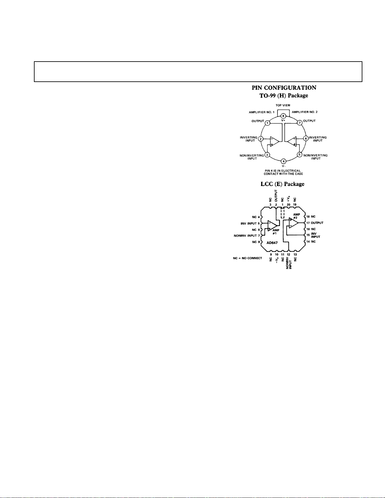
Standard Dual Amplifier Pinout
Available in Hermetic Metal Can Package, Hermetic
Surface Mount (20-Pin LCC) and Chip Form
MIL-STD-883B Processing Also Available
Single Version Available: AD547
Dual BiFET Op Amp
AD647
PRODUCT DESCRIPTION
The AD647 is an ultralow drift, dual JFET amplifier that combines high performance and convenience in a single package.
The AD647 uses the most advanced ion-implantation and laser
wafer drift trimming technologies to achieve the highest performance currently available in a dual JFET. Ion-implantation permits the fabrication of matched JFETs on a monolithic bipolar
chip. Laser wafer drift trimming trims both the initial offset voltage and its drift with temperature to provide offsets as low as
100 µV (250 µV max) and drifts of 2.5 µV/°C max.
In addition to outstanding individual amplifier performance, the
AD647 offers guaranteed and tested matching performance on
critical parameters such as offset voltage, offset voltage drift and
bias currents.
The high level of performance makes the AD647 especially well
suited for high precision instrumentation amplifier applications
that previously would have required the costly selection and
matching of space wasting single amplifiers.
The AD647 is offered in four performance grades, three commercial (the J, K and L) and one extended (the S). All are supplied in hermetically sealed 8-pin TO-99 packages and are
available processed to MIL-STD-883B. The LCC version is
also available processed to MIL-STD-883B.
REV. A
Information furnished by Analog Devices is believed to be accurate and
reliable. However, no responsibility is assumed by Analog Devices for its
use, nor for any infringements of patents or other rights of third parties
which may result from its use. No license is granted by implication or
otherwise under any patent or patent rights of Analog Devices.
PRODUCT HIGHLIGHTS
1. The AD647 is guaranteed and tested to tight matching specifications to ensure high performance and to eliminate the selection and matching of single devices.
2. Laser wafer drift trimming reduces offset voltage and offset
voltage drifts to 250 µV and 2.5 µV/°C max.
3. Voltage noise is guaranteed at 4 µV p-p max (0.1 Hz to
10 Hz) on K, L and S grades.
4. Bias current (35 pA K, L, S; 75 pA J) is specified after five
minutes of operation.
5. Total supply current is a low 2.8 mA max.
6. High open loop gain ensures high linearity in precision instrumentation amplifier applications.
7. The standard dual amplifier pinout permits the direct substitution of the AD647 for lower performance devices.
8. The AD647 is available in chip form.
One Technology Way, P.O. Box 9106, Norwood, MA 02062-9106, U.S.A.
Tel: 617/329-4700 Fax: 617/326-8703
Page 2
AD647–SPECIFICATIONS
(@ +258C and VS = 615 V dc)
Model AD647J AD647K AD647L AD647S
Min Typ Max Min Typ Max Min Typ Max Min Typ Max Units
OPEN LOOP GAIN
VO = ± 10 V, RL ≥ 2 kΩ 100,000 250,000 250,000 250,000 V/V
T
to T
MIN
, RL = 2 kΩ 100,000 250,000 250,000 100,000 V/V
MAX
OUTPUT CHARACTERISTICS
Voltage @ R
Voltage @ R
Short Circuit Current 25 25 25 25 mA
= 2 kΩ, T
L
= 10 kΩ, T
L
MIN
MIN
to T
to T
610 ±12 610 ±12 610 ±12 610 ±12 V
MAX
612 ±13 612 ±13 612 ±13 612 ±13 V
MAX
FREQUENCY RESPONSE
Unity Gain Small Signal 1.0 1.0 1.0 1.0 MHz
Full Power Response 50 50 50 50 kHz
Slew Rate, Unity Gain 2.0 3.0 2.0 3.0 2.0 3.0 2.0 3.0 V/µs
INPUT OFFSET VOLTAGE
1
Initial Offset 1.0 0.5 0.25 0.5 mV
Input Offset Voltage vs. Temperature 10 5 2.5 5.0 µV/°C
Input Offset Voltage vs. Supply,
T
to T
MIN
MAX
INPUT BIAS CURRENT
2
200 100 100 100 µV/V
Either Input 10 75 10 35 10 35 10 35 pA
Offset Current 5222pA
MATCHING CHARACTERISTICS
3
Input Offset Voltage 1.0 0.5 0.25 0.5 mV
Input Offset Voltage T
Input Bias Current 35 25 25 25 pA
MIN
to T
MAX
10 5 2.5 10.0 µV/°C
Crosstalk –124 –124 –124 –124 dB
INPUT IMPEDANCE
Differential 10
Common Mode 1012i610
INPUT VOLTAGE RANGE
Differential
4
12
i610
12
i610
12
i610
12
i610
12
i610
12
i6MΩipF
12
i6MΩipF
±20 ±20 ±20 ±20 V
Common Mode 610 ±12 610 ±12 610 ±12 610 ±12 V
Common-Mode Rejection 76 80 80 80 dB
INPUT NOISE
Voltage 0.1 Hz to 10 Hz 2 444µV p-p
f = 10 Hz 70 70 70 70 nV/√Hz
f = 100 Hz 45 45 45 45 nV/√Hz
f = 1 kHz 30 30 30 30 nV/√
Hz
f = 10 kHz 25 25 25 25 nV/√Hz
POWER SUPPLY
Rated Performance ± 15 ±15 ± 15 ±15 V
Operating ± 5 ±18 ±5 ±18 ±5 ± 18 ± 5 ±18 V
Quiescent Current 2.8 2.8 2.8 2.8 mA
TEMPERATURE RANGE
Operating, Rated Performance 0 +70 0 +70 0 +70 –55 +125 °C
Storage –65 +150 –65 +150 –65 +150 –65 +150 °C
PACKAGE OPTION
TO-99 Style (H-08B) AD647JH AD647KH AD647LH AD647SH
LCC (E-20A) AD647SE
AD647SE/883BH
NOTES
1
Input Offset Voltage specifications are guaranteed after 5 minutes of operation at TA = +25°C.
2
Bias Current specifications are guaranteed at maximum at either input after 5 minutes of operation at TA = +25°C. For higher temperatures, the current doubles every 10°C.
3
Matching is defined as the difference between parameters of the two amplifiers.
4
Defined as the maximum safe voltage between inputs, such that neither exceeds ±10 V from ground.
Specifications shown in boldface are tested on all production units at final electrical test. Results from those tests are used to calculate outgoing quality levels. All min and max specifications
are guaranteed, although only those shown in boldface are tested on all production units.
Specifications subject to change without notice.
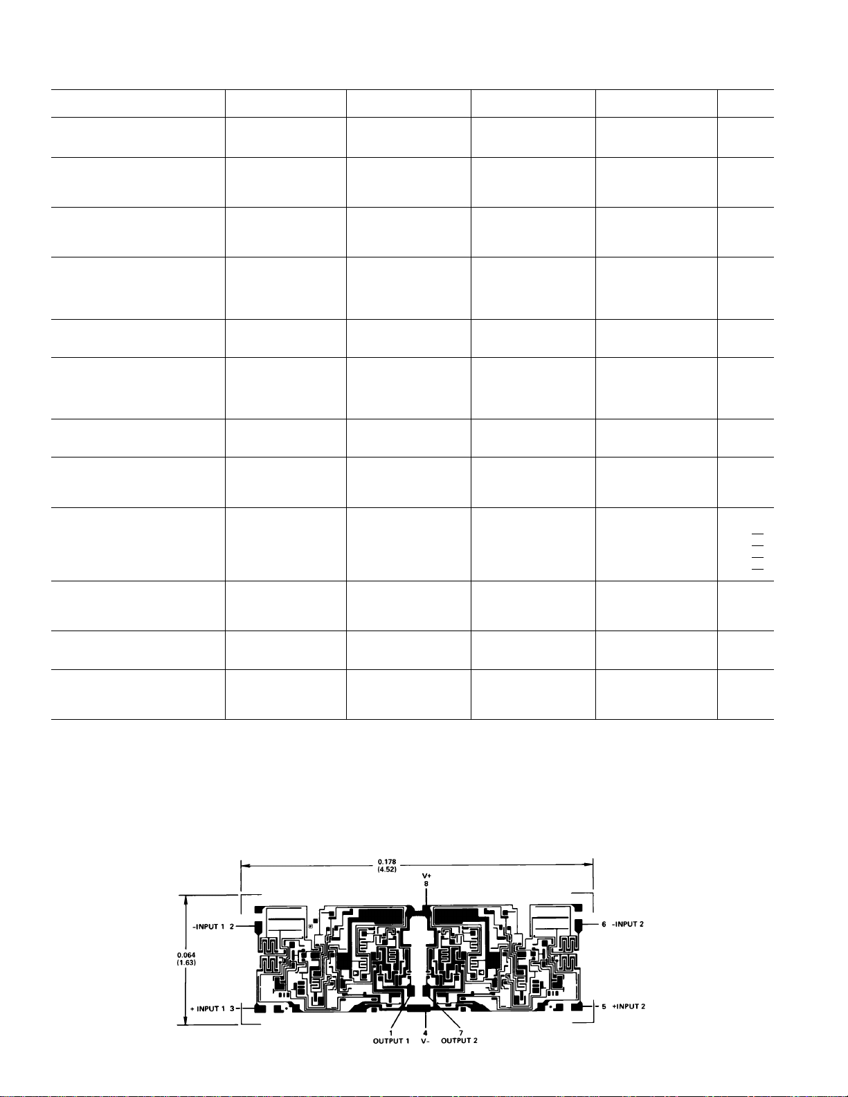
METALIZATION PHOTOGRAPH
Dimensions shown in inches and (mm).
Contact factory for latest dimensions.
–2–
REV. A
Page 3

Typical Characteristics–AD647
REV. A
–3–
Page 4

AD647
–4–
REV. A
Page 5

AD647
APPLICATION NOTES
The AD647 is fully specified under actual operating conditions
to insure high performance in any application, but there are some
steps that will improve on even this high level of performance.
The bias current of a JFET amplifier doubles with every 10°C
increase in junction temperature. Any heat source that can be
eliminated or minimized will significantly improve bias current
performance. To account for normal power dissipation, the largest contributor to chip self-heating, the bias currents of the
AD647 are guaranteed fully warmed up with ± 15 V supplies. A
decrease in supply voltage will decrease power consumption,
resulting in a corresponding drop in bias currents.
Open loop gain and bias currents, to some extent, are affected
by output loading. In applications where high linearity is essential, load impedance should be kept as high as possible to minimize degradation of open loop gain.
The outstanding ac and dc performance of the AD647 make it
an ideal choice for critical instrumentation applications. In such
applications, leakage paths, line losses and external noise
sources should be considered in the layout of printed circuit
boards. A guard ring surrounding the inputs and connected to a
low impedance potential (at the same level as the inputs) should
be placed on both sides of the circuit board. This will eliminate
leakage paths that could degrade bias current performance. All
signal paths should be shielded to minimize noise pickup.
THE AD647 USED WITH THE AD7546
Figure 24 shows the AD647 used with the AD7546 16-bit
segment DAC. In this application, amplifier performance is
critical to the overall performance of the AD7546. A1 is used as
a dual precision buffer. Here the offset voltage match, low offset
voltage and high open loop gain of the AD647 ensure monotonicity and high linearity over the entire operating temperature
range. A2 serves a dual function amplifier A is a Track and
Hold circuit that deglitches the DAC output and amplifier B
acts as an output amplifier. The performance of the amplifiers
of A2 is crucial to the accuracy of the system. The errors of
these amplifiers are added to the errors due strictly to DAC imperfections. For this reason great care should be used in the selection of these amplifiers. The matching characteristics, low
bias current and low temperature coefficients of the AD647
make it ideal for this application.
Figure 23. AD647 Used as DAC Output Amplifier
A CMOS DAC AMPLIFIER
The output impedance of a CMOS DAC, such as the AD7541,
varies with digital input code. This causes a corresponding
variation in the noise gain of the DAC-amplifier combination.
This noise gain modulation introduces a nonlinearity whose
magnitude is dependent on the amount of offset voltage present.
Laser wafer drift trimming lowers the initial offset voltage and
the offset voltage drift of the AD647, therefore minimizing the
effect of this nonlinearity and its drift with temperature. This, in
conjunction with the low bias current and high open loop gain,
makes the AD647 ideal for DAC output amplifier applications.
Figure 24. AD647 Used with AD7546 16-Bit DAC
USING THE AD647 IN LOG AMPLIFIER APPLICATIONS
Log amplifiers or log ratio amplifiers are useful in a wide range
of analog computational applications, ranging from the simple
linearization of exponential transducer outputs to the use of
logarithms in computations involving multi-term products or arbitrary exponents. Log amps also facilitate the compression of
wide ranging analog input signals into a range that can be easily
handled using standard circuit techniques.
Figure 25. Log-Ratio Amplifier
REV. A –5–
Page 6

AD647
The picoamp level input current and low offset voltage of the
AD647 make it suitable for wide dynamic range log amplifiers.
Figure 25 is a schematic of a log ratio circuit employing the
AD647 that can achieve less than 1% conformance error over
5 decades of current input, 1 nA to 100 µA. For voltage inputs,
the dynamic range is typically 50 mV to 10 V for 1% error,
limited on the low end by the amplifiers’ input offset voltage.
The conversion between current (or voltage) input and log output is accomplished by the base-emitter junctions of the dual
transistor Q1. Assuming Q1 has β > 100, which is the case for
the specified transistor, the base-emitter voltage on side 1 is to a
close approximation
V
= kT/q ln I1/I
BE A
S1
This circuit is arranged to take the difference of the VBEs of Q1A
and Q1B, thus producing an output voltage proportional to the
log of the ratio of the inputs
V
= –K (VBE A – VBE B) =
OUT
V
OUT
= –K kT/q ln Il /I
KkT
(ln I1/IS1 –ln I2/IS2)
q
2
The scaling constant, K is set by R1 and RTC to about 16, to
produce a 1 V change in output voltage per decade difference in
input signals. R
is a special resistor with a +3500 ppm/°C
TC
temperature coefficient, which makes K inversely proportional
to temperature, compensating for the “T” in kT/q. The log ratio
transfer characteristic is therefore independent of temperature.
This particular log ratio circuit is free from the dynamic problems that plague many other log circuits. The –3 dB bandwidth
is 50 kHz over the top 3 decades, 100 nA to 100 µA, and de-
creases smoothly at lower input levels. This circuit needs no
additional frequency compensation for stable operation from
input current sources, such as photodiodes, which may have
100 pF of shunt capacitance. For larger input capacitances a
20 pF integration capacitor around each amplifier will provide a
smoother frequency response.
This log ratio amplifier can be readily adjusted for optimum
accuracy by following this simple procedure. First, apply V1 =
V2 = –10.00 V and adjust “Balance” for V
apply V1 = –10.00 V, V2 = –100 V and adjust gain for V
= 0.00 V. Next
OUT
OUT
=
+1.00 V. Repeat this procedure until gain and balance readings
are within 2 mV of ideal values.
ACTIVE FILTERS
In active low-pass filtering applications the dc accuracy of the
amplifiers used is critical to the performance of the filter cir-
cuits. DC error sources such as offset voltage and bias currents
represent the largest individual contributors to output error.
Offset voltages will be passed by the filtering network and may,
depending on the design of the filter circuit, be amplified and
generate unacceptable output offset voltages. In filter circuits for
low frequency ranges large value resistors are used to generate
the low-pass filter function. Input bias currents passing through
these resistors will generate an additional offset voltage that will
also be passed to the output of the filter.
The use of the AD647 will minimize these error sources and,
therefore, maximize filter accuracy. The wide variety of performance levels of the AD647 allows for just the amount of accuracy required for any given application.
AD647 AS AN INSTRUMENTATION AMPLIFIER
The circuit shown in Figure 26 uses the AD647 to construct an
ultra high precision instrumentation amplifier. In this type of
application the matching characteristics of a monolithic dual
amplifier are crucial to ensure high performance.
Figure 26. Precision FET Input Instrumentation Amplifier
The use of an AD647L as the input amplifier A1, guarantees
maximum offset voltage of 250 µV, drift of 2.5 µV/°C and bias
currents of 35 pA. A2 serves two less critical functions in the
amplifier and, therefore can be an AD647J. Amplifier A is an active data guard which increases ac CMRR and minimizes extraneous signal pickup and leakage. Amplifier B is the output
amplifier of the instrumentation amplifier. To attain the precision available from this configuration, a great deal of care
should be taken when selecting the external components.
CMRR will depend on the matching of resistors R1, R2, R3,
and R4. The gain drift performance of this circuit will be affected by the matching TC of the resistors used.
C683a–3–2/84
OUTLINE DIMENSIONS
Dimensions shown in inches and (mm).
TO-99 E-20A
–6–
PRINTED IN U.S.A.
REV. A
 Loading...