

Page 1
Low Noise, Low Drift
INPUT OFFSET VOLTAGE DRIFT– µV/°C
–0.5–2.0
1.0 1.5 2.5
–2.5 –1.5 –1.0
0.5 2.0
0.0
NUMBER OF UNITS
0
15
5
10
30
25
20
OUTPUT
V
–
NOTE: CASE IS CONNECTED
TO PIN 8
OFFSET
NULL
IN+
IN–
CASE
3
4
5
6
7
8
AD645
1
2
OFFSET
NULL
+V
8
7
6
5
TOP VIEW
AD645
1
4
2
3
NC = NO CONNECT
OFFSET
NULL
–IN
NC
OUTPUT
OFFSET
NULL
–V
S
+IN
+V
S
a
FEATURES
Improved Replacement for Burr-Brown
OPA-111 and OPA-121 Op Amp
LOW NOISE
2 mV p-p max, 0.1 Hz to 10 Hz
10 nV/√
11 fA p-p Current Noise 0.1 Hz to 10 Hz
HIGH DC ACCURACY
250 mV max Offset Voltage
1 mV/8C max Drift
1.5 pA max Input Bias Current
114 dB Open-Loop Gain
Available in Plastic Mini-DIP, 8-Pin Header Packages, or
APPLICATIONS
Low Noise Photodiode Preamps
CT Scanners
Precision I-V Converters
PRODUCT DESCRIPTION
The AD645 is a low noise, precision FET input op amp. It offers the pico amp level input currents of a FET input device
coupled with offset drift and input voltage noise comparable to a
high performance bipolar input amplifier.
The AD645 has been improved to offer the lowest offset drift in
a FET op amp, 1 µV/°C. Offset voltage drift is measured and
trimmed at wafer level for the lowest cost possible. An inherently low noise architecture and advanced manufacturing techniques result in a device with a guaranteed low input voltage
noise of 2 µV p-p, 0.1 Hz to 10 Hz. This level of dc performance
along with low input currents make the AD645 an excellent
choice for high impedance applications where stability is of
prime concern.
Hz max at 10 kHz
Chip Form
1k
IMPROVED
DRIFT
FET Op Amp
AD645
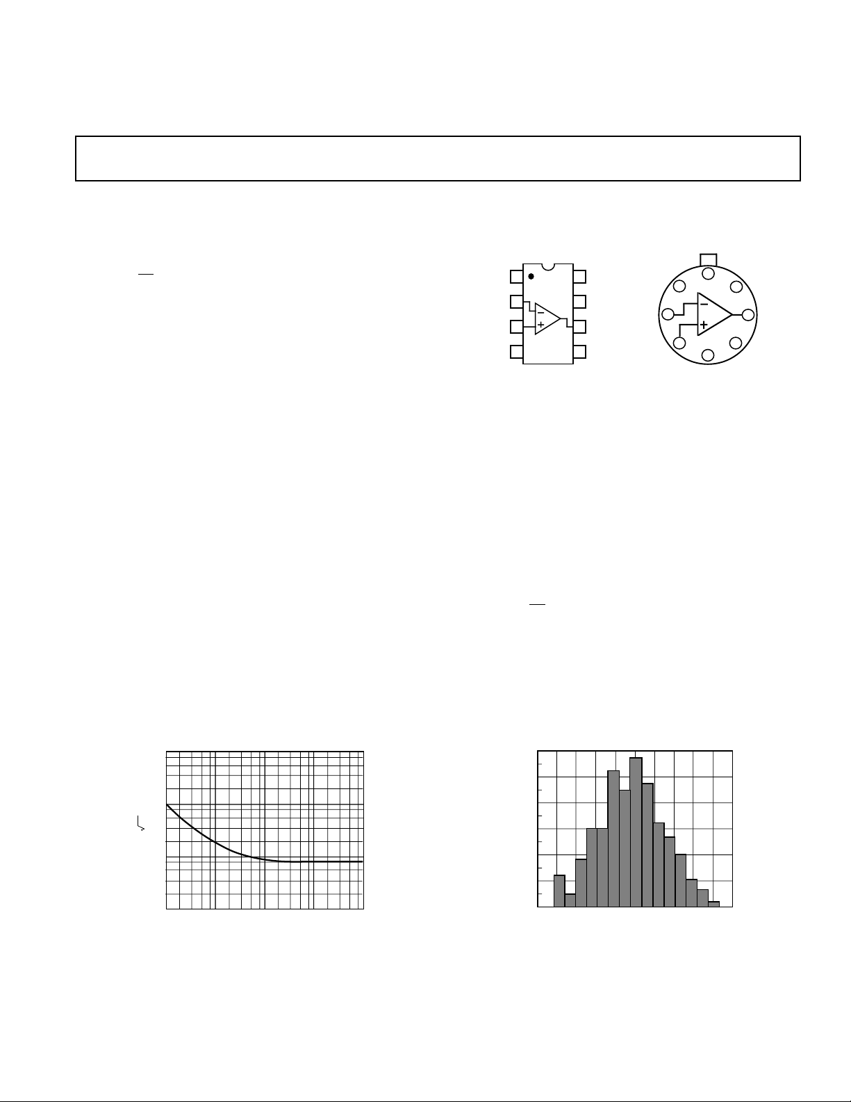
CONNECTION DIAGRAMS
8-Pin Plastic Mini-DIP
(N) Package
The AD645 is available in six performance grades. The AD645J
and AD645K are rated over the commercial temperature range
of 0°C to +70°C. The AD645A, AD645B, and the ultraprecision AD645C are rated over the industrial temperature
range of –40°C to +85°C. The AD645S is rated over the military
temperature range of –55°C to +125°C and is available
processed to MIL-STD-883B.
The AD645 is available in an 8-pin plastic mini-DIP, 8-pin
header, or in die form.
PRODUCT HIGHLIGHTS
1. Guaranteed and tested low frequency noise of 2 µV p-p max
and 20 nV/√
Hz at 100 Hz makes the AD645C ideal for low
noise applications where a FET input op amp is needed.
2. Low V
drift of 1 µV/°C max makes the AD645C an excel-
OS
lent choice for applications requiring ultimate stability.
3. Low input bias current and current noise (11 fA p-p 0.1 Hz to
10 Hz) allow the AD645 to be used as a high precision
preamp for current output sensors such as photodiodes, or as
a buffer for high source impedance voltage output sensors.
TO-99 (H) Package
100
nV/ Hz
10
VOLTAGE NOISE SPECTRAL DENSITY
1.0
FREQUENCY – Hz
Figure 1. AD645 Voltage Noise Spectral Density vs.
Frequency
REV. B
Information furnished by Analog Devices is believed to be accurate and
reliable. However, no responsibility is assumed by Analog Devices for its
use, nor for any infringements of patents or other rights of third parties
which may result from its use. No license is granted by implication or
otherwise under any patent or patent rights of Analog Devices.
1k1 10 100
10k
Figure 2. Typical Distribution of Average Input Offset
Voltage Drift (196 Units)
One Technology Way, P.O. Box 9106, Norwood, MA 02062-9106, U.S.A.
Tel: 617/329-4700 Fax: 617/326-8703
Page 2

AD645–SPECIFICATIONS
(@ +258C, and 615 V dc, unless otherwise noted)
Model AD645J/A AD645K/B AD645C AD645S
Conditions
INPUT OFFSET VOLTAGE
1
1
Min Typ Max Min Typ Max Min Typ Max Min Typ Max Units
Initial Offset 100 500 50 250 50 250 100 500 µV
Offset T
MIN–TMAX
300 1000 100 400 75 300 500 1500 µV
Drift (Average) 3 10/5 1 5/2 0.5 1 4 10 µV/°C
vs. Supply (PSRR) 90 110 94 110 94 110 90 110 dB
vs. Supply T
INPUT BIAS CURRENT
2
MIN–TMAX
100 90 100 90 100 86 95 dB
Either Input VCM = 0 V 0.7/1.8 3/5 0.7/1.8 1.5/3 1.8 3 1.8 5 pA
Either Input
@ T
MAX
VCM = 0 V 16/115 16/115 115 1800 pA
Either Input VCM = +10 V 0.8/1.9 0.8/1.9 1.9 1.9 pA
Offset Current VCM = 0 V 0.1 1.0 0.1 0.5 0.1 0.5 0.1 1.0 pA
Offset Current
@ T
MAX
VCM = 0 V 2/6 2/6 6 100 pA
INPUT VOLTAGE NOISE 0.1 to 10 Hz 1.0 3.0 1.0 2.5 1 2 1.0 3.3 µV p-p
f = 10 Hz 20 50 20 40 20 40 20 50 nV/√Hz
f = 100 Hz 10 30 10 20 10 20 10 30 nV/√Hz
f = 1 kHz 9 15 9 12 9 12 9 15 nV/√Hz
f = 10 kHz 8 10 8 10 8 10 8 10 nV/√Hz
INPUT CURRENT NOISE f = 0.1 to 10 Hz 11 20 11 15 11 15 11 20 fA p-p
f = 0.1 thru 20 kHz 0.6 1.1 0.6 0.8 0.6 0.8 0.6 1.1 fA/√Hz
FREQUENCY RESPONSE
Unity Gain, Small Signal 2 2 2 2 MHz
Full Power Response VO = 20 V p-p
R
= 2 kΩ 16 32 16 32 16 32 16 32 kHz
Slew Rate, Unity Gain V
SETTLING TIME
3
LOAD
= 20 V p-p
OUT
R
= 2 kΩ 12 12 12 12 V/µs
LOAD
To 0.1% 6 6 6 6 µs
To 0.01% 8 8 8 8 µs
Overload Recovery
4
50% Overdrive 5 5 5 5 µs
Total Harmonic f = 1 kHz
Distortion R
LOAD
≥ 2 kΩ
VO = 3 V rms 0.0006 0.0006 0.0006 0.0006 %
INPUT IMPEDANCE
Differential V
= ±1 V 1012i110
DIFF
12
i110
12
i110
12
i1 ΩipF
Common-Mode 1014i2.2 1014i2.2 1014i2.2 1014i2.2 ΩipF
INPUT VOLTAGE RANGE
Differential
5
±20 ±20 ±20 ±20 V
Common-Mode Voltage ± 10 +11, –10.4 ±10 +11, –10.4 ±10 +11, –10.4 ±10 +11, –10.4 V
Over Max Oper. Range ±10 ±10 ±10 ±10 V
Common-Mode
Rejection Ratio VCM = ±10 V 90 110 94 110 94 110 90 110 dB
T
MIN–TMAX
100 90 100 90 100 86 100 dB
OPEN-LOOP GAIN VO = ±10 V
R
≥ 2 kΩ 114 130 120 130 120 130 114 130 dB
LOAD
T
MIN–TMAX
114 114 110 dB
OUTPUT CHARACTERISTICS
Voltage R
Current V
≥ 2 kΩ±10 ±11 ±10 ±11 ±10 ±11 ±10 ±11 V
LOAD
T
MIN–TMAX
= ±10 V ±5 ± 10 ±5 ±10 ±5 ±10 ±5 ±10 mA
OUT
±10 ±10 ±10 ±10 V
Short Circuit ±15 ±15 ±15 ±15 mA
POWER SUPPLY
Rated Performance ±15 ±15 ± 15 ±15 V
Operating Range ±5 ±18 ±5 ±18 ±5 ±18 ±5 ±18 V
Quiescent Current 3.0 3.5 3.0 3.5 3.0 3.5 3.0 3.5 mA
Transistor Count # of Transistors 62 62 62 62
NOTES
1
Input offset voltage specifications are guaranteed after 5 minutes of operation at TA = +25°C.
2
Bias current specifications are guaranteed maximum at either input after 5 minutes of operation at T
3
Gain = –1, R
4
Defined as the time required for the amplifier’s output to return to normal operation after removal of a 50% overload from the amplifier input.
5
Defined as the maximum continuous voltage between the inputs such that neither input exceeds ±10 V from ground.
LOAD
= 2 kΩ.
= +25°C. For higher temperature, the current doubles every 10°C.
A
All min and max specifications are guaranteed.
Specifications subject to change without notice.
–2–
REV. B
Page 3
AD645
INPUT VOLTAGE NOISE – µV p-p
25
20
15
10
5
0
NUMBER OF UNITS
0.4 1.0
1.2
1.4
1.6
1.80.6 0.8
WARNING!
ESD SENSITIVE DEVICE
ABSOLUTE MAXIMUM RATINGS
Supply Voltage . . . . . . . . . . . . . . . . . . . . . . . . . . . . . . . . ±18 V
Internal Power Dissipation
2
(@ T
8-Pin Header Package . . . . . . . . . . . . . . . . . . . . . . 500 mW
8-Pin Mini-DIP Package . . . . . . . . . . . . . . . . . . . . 750 mW
Input Voltage . . . . . . . . . . . . . . . . . . . . . . . . . . . . . . . . . . . ±V
Output Short Circuit Duration . . . . . . . . . . . . . . . . Indefinite
Differential Input Voltage . . . . . . . . . . . . . . . . . . +V
Storage Temperature Range (H) . . . . . . . . . –65°C to +150°C
Storage Temperature Range (N) . . . . . . . . . –65°C to +125°C
Operating Temperature Range
AD645J/K . . . . . . . . . . . . . . . . . . . . . . . . . . . 0°C to +70°C
1
= +25°C)
A
and –V
S
AD645A/B/C . . . . . . . . . . . . . . . . . . . . . . . –40°C to +85°C
AD645S . . . . . . . . . . . . . . . . . . . . . . . . . . –55°C to +125°C
Lead Temperature Range
(Soldering 60 sec) . . . . . . . . . . . . . . . . . . . . . . . . . . . +300°C
NOTES
1
S
Stresses above those listed under “Absolute Maximum Ratings” may cause
permanent damage to the device. This is a stress rating only and functional
operation of the device at these or any other conditions above those indicated
S
in the operational section of this specification is not implied. Exposure to
absolute maximum rating conditions for extended periods may affect device
reliability.
2
Thermal Characteristics:
8-Pin Plastic Mini-DIP Package: θJA = 100°C/Watt
8-Pin Header Package: θJA = 200°C/Watt
CAUTION
ESD (electrostatic discharge) sensitive device. Electrostatic charges as high as 4000 V readily
accumulate on the human body and test equipment and can discharge without detection.
Although the AD645 features proprietary ESD protection circuitry, permanent damage may
occur on devices subjected to high energy electrostatic discharges. Therefore, proper ESD
precautions are recommended to avoid performance degradation or loss of functionality.
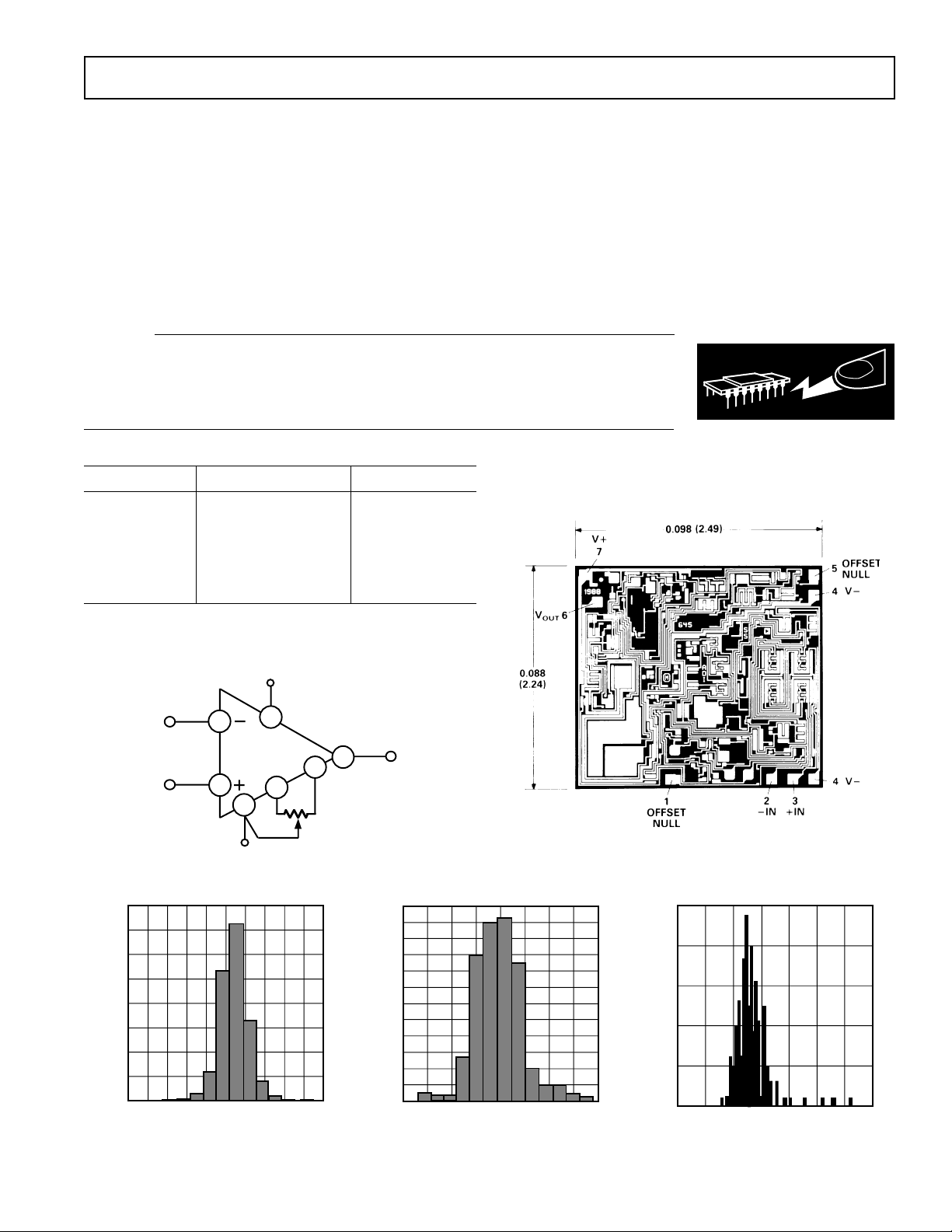
METALIZATION PHOTOGRAPH
Dimensions shown in inches and (mm).
Contact factory for latest dimensions.
Model
ORDERING GUIDE
1
Temperature Range Package Option
2
AD645JN 0°C to +70°C N-8
AD645KN 0°C to +70°C N-8
AD645AH –40°C to +85°C H-08A
AD645BH –40°C to +85°C H-08A
AD645CH –40°C to +85°C H-08A
AD645SH/883B –55°C to +125°C H-08A
NOTES
1
Chips are also available.
2
N = Plastic Mini-DIP; H = Metal Can.
+V
S
800
700
600
500
400
300
NUMBER OF UNITS
200
100
0
–1.0 0.8–0.4 –0.2 0.0 0.4 0.6 1.0–0.6 0.2–0.8
Figure 4. Typical Distribution of Input
Offset Voltage (1855 Units)
REV. B
AD645
4
–V
S
7
1
5
10k
V ADJUST
OS
6
2
3
Figure 3. AD645 Offset Null Configuration
120
110
100
90
80
70
60
50
40
NUMBER OF UNITS
30
20
10
0
0.0 0.5 1.0 1.5 2.0 2.5 3.0 3.5 4.0
INPUT OFFSET VOLTAGE – mV
Figure 5. Typical Distribution of Input
Bias Current (576 Units)
INPUT BIAS CURRENT – pA
Figure 6. Typical Distribution of 0.1 Hz
to 10 Hz Voltage Noise (202 Units)
–3–
Page 4

AD645–Typical Characteristics
VOLTAGE NOISE SPECTRAL DENSITY @ 1kHz – nV/
√
Hz
100
1k 10k 100k
1.0
10
100
SOURCE RESISTANCE – Ω
1M 10M 100M
1k
SOURCE
RESISTANCE
NOISE OF AD645
AND RESISTOR
RESISTOR NOISE
ONLY
(@ +258C, 615 V unless otherwise noted)
100
Hz
√
10
1.0
CURRENT NOISE SPECTRAL DENSITY – fA/
0.1
1
100
10
1k 10k 100k
FREQUENCY – Hz
Figure 7. Current Noise Spectral
Density vs. Frequency
1k
100
NOISE BANDWIDTH: 0.1 to 10Hz
1k
100
10
VOLTAGE NOISE SPECTRAL DENSITY – nV/ Hz
0
1M
1 10 100 1k 10k 100k
FREQUENCY – Hz
Figure 8. Voltage Noise Spectral
Density vs. Frequency
1000
R = 10MΩ
Hz
100
10
VOLTAGE NOISE SPECTRAL DENSITY – nV
1
0.1
1.0
10 100
FREQUENCY – Hz
S
R = 1MΩ
S
R = 100kΩ
S
R = 100Ω
S
1k 10k
Figure 9. Voltage Noise Spectral
Density vs. Frequency for Various
100k
Source Resistances
25
f = 1kHz
o
20
Hz
√
nV/
–
15
CURRENT NOISE
100
10
1
Hz
√
10
INPUT VOLTAGE NOISE – µV p-p
1.0
10310
4
5
10
SOURCE RESISTANCE – Ω
7
6
10
8
10
10
Figure 10. Input Voltage Noise vs.
Source Resistance
10
VOLTAGE NOISE
10
5
–
–
9
60
VOLTAGE NOISE
040–20
20 40 60 80 100 120 140
TEMPERATURE – C
Figure 11. Voltage and Current
Noise Spectral Density vs.
Temperature
50
T = +25 C
A
V = ±15V
25
0
–
25
CHANGE IN INPUT OFFSET VOLTAGE – µV
–
50
0
1
WARM-UP TIME – Minutes
S
2345
Figure 13. Change in Input Offset
Voltage vs. Warmup Time
150
75
TA = 25°C TO TA = 85°C
0
–
75
CHANGE IN INPUT OFFSET VOLTAGE – µV
150–
012 345
TIME FROM THERMAL SHOCK – Minutes
Figure 14. Change in Input Offset
Voltage vs. Time from Thermal
Shock
CURRENT NOISE – fA/
0.1
0.01
Figure 12. Voltage Noise Spectral
Density @ 1 kHz vs. Source
Resistance
–
9
10
–
10
10
–
11
10
–
12
10
INPUT BIAS CURRENT – Amps
–
13
10
–
14
10
–– –
60 40 20 0 20 40 60
INPUT
BIAS
CURRENT
TEMPERATURE – C
INPUT
OFFSET
CURRENT
80 100
140
120
Figure 15. Input Bias and Offset
Currents vs. Temperature
–
9
10
–
10
10
–
11
10
–
12
10
–
13
INPUT OFFSET CURRENT – Amps
10
–
14
10
–4–
REV. B
Page 5

AD645
100 1k
10k 100k
FREQUENCY – Hz
1M 10M
100
80
60
40
20
0
120
101
COMMON-MODE REJECTION – dB
SLEW RATE – Volts/µs
60 40
20
0
20
40 60 80 100 120 140
1.0
2.0
3.0
4.0
3.0
2.0
1.0
GAIN-BANDWIDTH PRODUCT – MHz
0
TEMPERATURE – 8 C
–––
GAIN-BANDWIDTH
SLEW RATE
35
30
25
20
15
10
5
0
OUTPUT VOLTAGE – Volts p-p
FREQUENCY – Hz
1M1k 10k 100k
10
TA = +25°C
V
= ±15V
S
H PACKAGE
1.0
INPUT BIAS CURRENT – pA
0.1
20–15–10–5
–
51015
0
COMMON MODE VOLTAGE – Volts
Figure 16. Input Bias Current vs.
Common-Mode Voltage
120
110
100
90
COMMON-MODE REJECTION – dB
80
70
–– –
10
15 15
COMMON MODE VOLTAGE – Volts
0510
5
Figure 19. Common-Mode
Rejection vs. Input Common-Mode
Voltage
120
100
80
60
40
POWER SUPPLY REJECTION – dB
20
0
–
PSRR
100 1k 10k 100k
101
FREQUENCY – Hz
+
PSRR
1M 10M
Figure 17. Power Supply Rejection
vs. Frequency
1M 10M
–
45
–
90
–
135
–
180
110
100
80
60
40
OPEN-LOOP GAIN – dB
20
0
–
20
100
10
PHASE
GAIN
1k 10k 100k
FREQUENCY – Hz
Figure 20. Open-Loop Gain and
Phase Shift vs. Frequency
Figure 18. Common-Mode
Rejection vs. Frequency
PHASE SHIFT – Degrees
Figure 21. Gain-Bandwidth Product
and Slew Rate vs. Temperature
4.0
3.0
2.0
GAIN-BANDWIDTH PRODUCT – MHz
1.0
0 5 10 15 20
Figure 22. Gain-Bandwidth and
Slew Rate vs. Supply Voltage
REV. B
SLEW RATE
GAIN-BANDWIDTH
SUPPLY VOLTAGE – ±Volts
160
V = ±15V
4.0
3.0
SLEW RATE – Volts/µs
2.0
150
140
130
120
OPEN-LOOP GAIN – dB
110
100
–– –
60 40 20 0 20 40 60 80 100 120 140
Figure 23. Open-Loop Gain vs.
Temperature
S
V = ±10V
O
RL = 2kΩ
TEMPERATURE –
–5–
8
C
Figure 24. Large Signal Frequency
Response
Page 6

AD645
AD645–Typical Characteristics
10
8
6
4
0.1% 0.01%
2
0
–
2
–
4
–
6
OUTPUT SWING FROM 0V TO ±VOLTS
–
8
–
10
1.0
ERROR
0.1%
2.0 3.0 4.0 5.0 6.0 7.0 8.0 9.0
0.01%
SETTLING TIME – µs
Figure 25. Output Swing and Error
vs. Settling Time
0.1µF
+
V
S
7
2
V
IN
AD645
3
6
4
0.1µF
–
V
S
RL
2kΩ
V
OUT
C
10pF
100
90
FOR 10V STEP
80
70
60
50
40
SETTLING TIME – µs
30
20
10
0
1
CLOSED-LOOP VOLTAGE GAIN (V/V)
0.01%
0.1%
10
100
1k
Figure 26. Settling Time vs. ClosedLoop Voltage Gain
L
4
3
2
SUPPLY CURRENT – mA
1
0
–60 –40 –20 0 20 40 60 80 100 120 140
TEMPERATURE – 8C
Figure 27. Supply Current vs.
Temperature
Figure 28a. Unity-Gain Follower
5kΩ
0.1µF
+
V
V
IN
5kΩ
2
AD645
3
–
S
7
6
4
0.1µF
V
S
2kΩ
RL
Figure 29a. Unity-Gain Inverter
V
OUT
C
L
10pF
Figure 28b. Unity-Gain Follower
Large Signal Pulse Response
Figure 29b. Unity-Gain Inverter
Large Signal Pulse Response
Figure 28c. Unity-Gain Follower
Small Signal Pulse Response
Figure 29c. Unity-Gain Inverter
Small Signal Pulse Response
–6–
REV. B
Page 7

AD645
V
OUT
=
i
n
2
+
i
f
2
+
i
s
2
Rf
1 + s (Cf ) Rf
2
+
en
2
1 +
Rf
Rd
1 + s (Cd ) Rd
1 + s (Cf ) Rf
2
FREQUENCY – Hz
100 1k 10k 100k101
10nV
100nV
1µV
10µV
SIGNAL BANDWIDTH
NO FILTER
WITH FILTER
e
n
is&i
f
i
n
en
OUTPUT VOLTAGE NOISE – Volts/ Hz
√
Preamplifier Applications
The low input current and offset voltage levels of the AD645 together with its low voltage noise make this amplifier an excellent
choice for preamplifiers used in sensitive photodiode applications. In a typical preamp circuit, shown in Figure 30, the output of the amplifier is equal to:
where:
An equivalent model for a photodiode and its dc error sources is
shown in Figure 31. The amplifier’s input current, I
tribute an output voltage error which will be proportional to the
value of the feedback resistor. The offset voltage error, V
cause a “dark” current error due to the photodiode’s finite
shunt resistance, Rd. The resulting output voltage error, V
equal to:
A shunt resistance on the order of 109 ohms is typical for a
small photodiode. Resistance Rd is a junction resistance which
will typically drop by a factor of two for every 10°C rise in temperature. In the AD645, both the offset voltage and drift are
low, this helps minimize these errors.
Minimizing Noise Contributions
The noise level limits the resolution obtainable from any preamplifier. The total output voltage noise divided by the feedback
resistance of the op amp defines the minimum detectable signal
current. The minimum detectable current divided by the photodiode sensitivity is the minimum detectable light power.
REV. B
10pF
9
10 Ω
GUARD
PHOTODIODE
2
AD645
3
6
8
OPTIONAL 26Hz
OUTPUT
FILTERED
OUTPUT
FILTER
Figure 30. The AD645 Used as a Sensitive Preamplifier
V
= ID (Rf) = Rp (P) Rf
OUT
= photodiode signal current (Amps)
I
D
Rp = photodiode sensitivity (Amp/Watt)
Rf = the value of the feedback resistor, in ohms.
P = light power incident to photodiode surface, in watts.
, will con-
B
, will
OS
, is
E
V
= (1 + Rf/Rd) V
E
PHOTODIODE
Rd
I
D
Cd
50pF
I
B
+ Rf I
OS
Cf
10pF
V
OS
Rf
10 Ω
B
9
OUTPUT
Figure 31. A Photodiode Model Showing DC Error
Sources
Sources of noise in a typical preamp are shown in Figure 32.
The total noise contribution is defined as:
Figure 33, a spectral density versus frequency plot of each
source’s noise contribution, shows that the bandwidth of the
amplifier’s input voltage noise contribution is much greater than
its signal bandwidth. In addition, capacitance at the summing
junction results in a “peaking” of noise gain in this configuration. This effect can be substantial when large photodiodes with
large shunt capacitances are used. Capacitor Cf sets the signal
bandwidth and also limits the peak in the noise gain. Each
source’s rms or root-sum-square contribution to noise is obtained by integrating the sum of the squares of all the noise
sources and then by obtaining the square root of this sum. Minimizing the total area under these curves will optimize the
preamplifier’s overall noise performance.
Cf
10pF
Rf
9
10 Ω
PHOTODIODE
Rd
i
S
Cd
i
S
50pF
en
i
f
i
n
OUTPUT
Figure 32. Noise Contributions of Various Sources
Figure 33. Voltage Noise Spectral Density of the Circuit of
Figure 32 With and Without an Output Filter
An output filter with a passband close to that of the signal can
greatly improve the preamplifier’s signal to noise ratio. The photodiode preamplifier shown in Figure 32—without a bandpass
filter—has a total output noise of 50 µV rms. Using a 26 Hz
single pole output filter, the total output noise drops to 23 µV
rms, a factor of 2 improvement with no loss in signal bandwidth.
Using a “T” Network
A “T” network, shown in Figure 34, can be used to boost the effective transimpedance of an I to V converter, for a given feedback resistor value. Unfortunately, amplifier noise and offset
voltage contributions are also amplified by the “T” network
gain. A low noise, low offset voltage amplifier, such as the
AD645, is needed for this type of application.
–7–
Page 8

AD645
45
°
BSC
0.100
(2.54)
BSC
0.034 (0.86)
0.027 (0.69)
0.045 (1.14)
0.027 (0.69)
0.160 (4.06)
0.110 (2.79)
0.100
(2.54)
BSC
0.200
(5.08)
BSC
6
8
5
7
1
4
2
3
REFERENCE PLANE
BASE & SEATING PLANE
0.335 (8.51)
0.305 (7.75)
0.370 (9.40)
0.335 (8.51)
0.750 (19.05)
0.500 (12.70)
0.045 (1.14)
0.010 (0.25)
0.050
(1.27)
MAX
0.040 (1.02) MAX
0.019 (0.48)
0.016 (0.41)
0.021 (0.53)
0.016 (0.41)
0.185 (4.70)
0.165 (4.19)
0.250 (6.35)
MIN
10pF
R
G
10kΩ
Rf
R
8
10 Ω
i
1.1kΩ
V
OUT
AD645
PHOTODIODE
R
G
V = I R (1 )
OUT+D
f
R
i
Figure 34. A Photodiode Preamp Employing a “T”
Network for Added Gain
A pH Probe Buffer Amplifier
A typical pH probe requires a buffer amplifier to isolate its 10
9
to 10
Ω source resistance from external circuitry. Just such an
6
amplifier is shown in Figure 35. The low input current of the
AD645 allows the voltage error produced by the bias current
and electrode resistance to be minimal. The use of guarding,
shielding, high insulation resistance standoffs, and other such
standard methods used to minimize leakage are all needed to
maintain the accuracy of this circuit.
The slope of the pH probe transfer function, 50 mV per pH unit
at room temperature, has a +3300 ppm/°C temperature coefficient. The buffer of Figure 35 provides an output voltage equal
to 1 volt/pH unit. Temperature compensation is provided by
resistor RT which is a special temperature compensation resistor, part number Q81, 1 kΩ, 1%, +3500 ppm/°C, available from
Tel Labs Inc.
Guarding the input lines by completely surrounding them with a
metal conductor biased near the input lines’ potential has two
major benefits. First, parasitic leakage from the signal line is
reduced, since the voltage between the input line and the guard
is very low. Second, stray capacitance at the input terminal is
minimized which in turn increases signal bandwidth. In the
header or can package, the case of the AD645 is connected to
Pin 8 so that it may be tied to the input potential (when operating as a follower) or tied to ground (when operating as an inverter). The AD645’s positive input (Pin 3) is located next to
the negative supply voltage pin (Pin 4). The negative input (Pin
2) is next to the balance adjust pin (Pin 1) which is biased at a
potential close to that of the negative supply voltage. Note that
any guard traces should be placed on both sides of the board. In
addition, the input trace should be guarded along both of its
edges, along its entire length.
Contaminants such as solder flux, on the board’s surface and on
the amplifier’s package, can greatly reduce the insulation resistance and also increase the sensitivity to atmospheric humidity.
Both the package and the board must be kept clean and dry. An
effective cleaning procedure is to: first, swab the surface with
high grade isopropyl alcohol, then rinse it with deionized water,
and finally, bake it at 80°C for 1 hour. Note that if either polystyrene or polypropylene capacitors are used on the printed circuit board that a baking temperature of 70°C is safer, since both
of these plastic compounds begin to melt at approximately
+85°C.
OUTLINE DIMENSIONS
Dimensions shown in inches and (mm).
TO-99 Header (H) Package
C1398a–24–9/91
0.1µF
0.1µF
°
C
+15V
COM
–15V
pH
PROBE
GUARD
V ADJUST
OS
100kΩ
–
1
4
3
AD645
2
8
+
+V
S
V
S
–V
S
OUTPUT
5
6
7
V
S
1VOLT/pH UNIT
19.6kΩ
RT
1kΩ
+3500ppm/
Figure 35. A pH Probe Amplifier
Circuit Board Notes
The AD645 is designed for through hole mount into PC boards.
Maintaining picoampere level resolution in that environment
requires a lot of care. Since both the printed circuit board and
the amplifier’s package have a finite resistance, the voltage difference between the amplifier’s input pin and other pins (or
traces on the PC board) will cause parasitic currents to flow into
(or out of) the signal path. These currents can easily exceed the
1.5 pA input current level of the AD645 unless special precautions are taken. Two successful methods for minimizing leakage
are: guarding the AD645’s input lines and maintaining adequate
insulation resistance.
–8–
PIN 1
0.210
(5.33)
MAX
0.160 (4.06)
0.115 (2.93)
0.022 (0.558)
0.014 (0.356)
Plastic Mini-DIP (N) Package
8
1
0.430 (10.92)
0.348 (8.84)
0.100
(2.54)
BSC
5
4
0.070 (1.77)
0.045 (1.15)
0.280 (7.11)
0.240 (6.10)
0.060 (1.52)
0.015 (0.38)
0.130
(3.30)
MIN
SEATING
PLANE
0.325 (8.25)
0.300 (7.62)
0.015 (0.381)
0.008 (0.204)
0.195 (4.95)
0.115 (2.93)
PRINTED IN U.S.A.
REV. B
 Loading...