

Page 1
Micropower, Single- and Dual-Supply,
–V
www.BDTIC.com/ADI
Rail-to-Rail Instrumentation Amplifier
FEATURES
Micropower, 85 µA maximum supply current
Wide power supply range (+2.2 V to ±18 V)
Easy to use
Gain set with one external resistor
Gain range 5 (no resistor) to 1000
Higher performance than discrete designs
Rail-to-rail output swing
High accuracy dc performance
0.03% typical gain accuracy (G = +5) (AD627A)
10 ppm/°C typical gain drift (G = +5)
125 µV maximum input offset voltage (AD627B dual supply)
200 µV maximum input offset voltage (AD627A dual supply)
1 µV/°C maximum input offset voltage drift (AD627B)
3 µV/°C maximum input offset voltage drift (AD627A)
10 nA maximum input bias current
Noise: 38 nV/√Hz RTI noise @ 1 kHz (G = +100)
Excellent ac specifications
AD627A: 77 dB minimum CMRR (G = +5)
AD627B: 83 dB minimum CMRR (G = +5)
80 kHz bandwidth (G = +5)
135 µs settling time to 0.01% (G = +5, 5 V step)
APPLICATIONS
4 to 20 mA loop-powered applications
Low power medical instrumentation—ECG, EEG
Transducer interfacing
Thermocouple amplifiers
Industrial process controls
Low power data acquisition
Portable battery-powered instruments
GENERAL DESCRIPTION
The AD627 is an integrated, micropower instrumentation
amplifier that delivers rail-to-rail output swing on single and
dual (+2.2 V to ±18 V) supplies. The AD627 provides excellent
ac and dc specifications while operating at only 85 µA maximum.
The AD627 offers superior flexibility by allowing the user to set
t
he gain of the device with a single external resistor while conforming to the 8-lead industry-standard pinout configuration.
With no external resistor, the AD627 is configured for a gain of 5.
With an external resistor, it can be set to a gain of up to 1000.
A wide supply voltage range (+2.2 V to ±18 V) and micropower
urrent consumption make the AD627 a perfect fit for a wide
c
range of applications. Single-supply operation, low power
consumption, and rail-to-rail output swing make the AD627
Rev. D
Information furnished by Analog Devices is believed to be accurate and reliable. However, no
responsibility is assumed by Anal og Devices for its use, nor for any infringements of patents or ot her
rights of third parties that may result from its use. Specifications subject to change without notice. No
license is granted by implication or otherwise under any patent or patent rights of Analog Devices.
Trademarks and registered trademarks are the property of their respective owners.
AD627
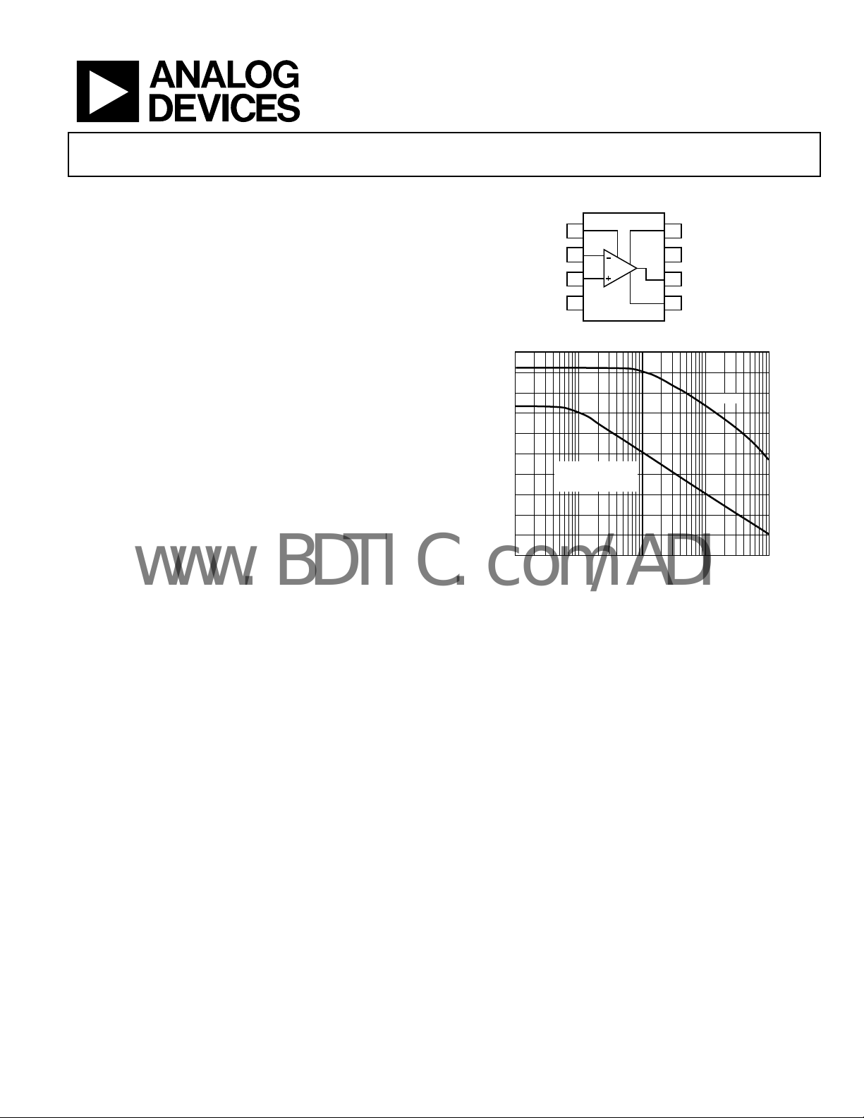
FUNCTIONAL BLOCK DIAGRAM
R
G
–IN
+IN
S
Figure 1. 8-Lead PDIP (N) and SOIC_N (R)
100
90
80
70
60
50
40
CMRR (dB)
30
20
10
0
1 10 100
DISCRETE DESI GN
Figure 2. CMRR vs. Frequency, ±5 V
ideal for battery-powered applications. Its rail-to-rail output
stage maximizes dynamic range when operating from low
supply voltages. Dual-supply operation (±15 V) and low power
consumption make the AD627 ideal for industrial applications,
including 4 to 20 mA loop-powered systems.
The AD627 does not compromise performance, unlike other
opower instrumentation amplifiers. Low voltage offset,
micr
offset drift, gain error, and gain drift minimize errors in the
system. The AD627 also minimizes errors over frequency by
providing excellent CMRR over frequency. Because the CMRR
remains high up to 200 Hz, line noise and line harmonics are
rejected.
The AD627 provides superior performance, uses less circuit
oard area, and costs less than micropower discrete designs.
b
One Technology Way, P.O. Box 9106, Norwood, MA 02062-9106, U.S.A.
Tel: 781.329.4700 www.analog.com
Fax: 781.461.3113 ©2007 Analog Devices, Inc. All rights reserved.
AD627
1
2
3
4
TRADITIONAL
LOW POWER
FREQUENCY ( Hz)
R
8
G
+V
7
S
OUTPUT
6
REF
5
1k 10k
, Gain = +5
S
AD627
00782-001
00782-002
Page 2

AD627
www.BDTIC.com/ADI
TABLE OF CONTENTS
Features.............................................................................................. 1
Applications....................................................................................... 1
Functional Block Diagram .............................................................. 1
General Description ......................................................................... 1
Revision History ............................................................................... 2
Specifications..................................................................................... 3
Single Supply................................................................................. 3
Dual Supply................................................................................... 5
Dual and Single Supplies ............................................................. 6
Absolute Maximum Ratings............................................................ 7
ESD Caution.................................................................................. 7
Pin Configurations and Function Descriptions ........................... 8
Typical Performance Characteristics ............................................. 9
Theory of Operation ...................................................................... 14
Using the AD627 ............................................................................15
Basic Connections ...................................................................... 15
Setting the Gain ..........................................................................15
Reference Terminal .................................................................... 16
Input Range Limitations in Single-Supply Applications....... 16
Output Buffering........................................................................ 17
Input and Output Offset Errors................................................ 17
Make vs. Buy: A Typical Application Error Budget............... 18
Errors Due to AC CMRR .......................................................... 19
Ground Returns for Input Bias Currents ................................ 19
Layout and Grounding .............................................................. 20
Input Protection ......................................................................... 21
RF Interference........................................................................... 21
Applications Circuits...................................................................... 22
Classic Bridge Circuit ................................................................ 22
4 to 20 mA Single-Supply Receiver.......................................... 22
Thermocouple Amplifier .......................................................... 22
Outline Dimensions....................................................................... 24
Ordering Guide .......................................................................... 24
REVISION HISTORY
11/07—Rev. C to Rev. D
Changes to Features.......................................................................... 1
Changes to Figure 29 to Figure 34 Captions............................... 13
Changes to Setting the Gain Section............................................ 15
Changes to Input Range Limitations in Single-Supply
Applications Section....................................................................... 16
Changes to Table 7.......................................................................... 17
Changes to Figure 41...................................................................... 18
11/05—Rev. B to Rev. C
pdated Format..................................................................Universal
U
Added Pin Configurations and Function
Descriptions Section ........................................................................ 8
Change to Figure 33 ....................................................................... 13
Updated Outline Dimensions....................................................... 24
Changes to Ordering Guide.......................................................... 24
Rev. A to Rev. B
hanges to Figure 4 and Table I, Resulting Gain column......... 11
C
Change to Figure 9 ......................................................................... 13
Rev. D | Page 2 of 24
Page 3

AD627
www.BDTIC.com/ADI
SPECIFICATIONS
SINGLE SUPPLY
Typical @ 25°C single supply, VS = 3 V and 5 V, and RL = 20 kΩ, unless otherwise noted.
Table 1.
AD627A AD627B
Parameter Conditions Min Typ Max Min Typ Max Unit
GAIN G = +5 + (200 kΩ/RG)
Gain Range 5 1000 5 1000 V/V
Gain Error
Nonlinearity
Gain vs. Temperature
VOLTAGE OFFSET
Input Offset, V
Output Offset, V
Offset Referred to the
INPUT CURRENT
Input Bias Current 3 10 3 10 nA
Input Offset Current 0.3 1 0.3 1 nA
INPUT
Input Impedance
Common-Mode Rejection
OUTPUT
Output Swing RL = 20 kΩ (−VS) + 25 (+VS) − 70 (−VS) + 25 (+VS) − 70 mV
R
Short-Circuit Current Short circuit to ground ±25 ±25 mA
1
G = +5 0.03 0.10 0.01 0.06 %
G = +10 0.15 0.35 0.10 0.25 %
G = +100 0.15 0.35 0.10 0.25 %
G = +1000 0.50 0.70 0.25 0.35 %
G = +5 10 100 10 100 ppm
G = +100 20 100 20 100 ppm
G = +5 10 20 10 20 ppm/°C
G > +5 −75 −75 ppm/°C
2
OSI
Over Temperature VCM = V
Average TC 0.1 3 0.1 1 µV/°C
1000 500 µV
OSO
Over Temperature 1650 1150 µV
Average TC 2.5 10 2.5 10 µV/°C
Input vs. Supply (PSRR)
G = +5 86 100 86 100 dB
G = +10 100 120 100 120 dB
G = +100 110 125 110 125 dB
G = +1000 110 125 110 125 dB
Over Temperature 15 15 nA
Average TC 20 20 pA/°C
Over Temperature 2 2 nA
Average TC 1 1 pA/°C
Differential 20||2 20||2 GΩ||pF
Common-Mode 20||2 20||2 GΩ||pF
Input Voltage Range3VS = 2.2 V to 36 V (−VS) − 0.1 (+VS) − 1 (−VS) − 0.1 (+VS) – 1 V
3
Ratio
DC to 60 Hz with
1 kΩ Source Imbalance
G = +5 VS = 3 V, VCM = 0 V to 1.9 V 77 90 83 96 dB
G = +5 VS = 5 V, VCM = 0 V to 3.7 V 77 90 83 96 dB
V
= (−VS) + 0.1 to (+VS) − 0.15
OUT
1
50 250 25 150 µV
= +VS/2 445 215 µV
REF
= VS/2
V
REF
= 100 kΩ (−VS) + 7 (+VS) − 25 (−VS) + 7 (+VS) − 25 mV
L
Rev. D | Page 3 of 24
Page 4

AD627
www.BDTIC.com/ADI
AD627A AD627B
Parameter Conditions Min Typ Max Min Typ Max Unit
DYNAMIC RESPONSE
Small Signal −3 dB
Bandwidth
G = +5 80 80 kHz
G = +100 3 3 kHz
G = +1000 0.4 0.4 kHz
Slew Rate +0.05/−0.07 +0.05/−0.07 V/µs
Settling Time to 0.01% VS = 3 V, 1.5 V output step
G = +5 65 65 µs
G = +100 290 290 µs
Settling Time to 0.01% VS = 5 V, 2.5 V output step
G = +5 85 85 µs
G = +100 330 330 µs
Overload Recovery 50% input overload 3 3 µs
1
Does not include effects of External Resistor RG.
2
See Table 8 for total RTI errors.
3
See the Using the AD627 section for more information on the input range, gain range, and common-mode range.
Rev. D | Page 4 of 24
Page 5

AD627
www.BDTIC.com/ADI
DUAL SUPPLY
Typical @ 25°C dual supply, VS = ±5 V and ±15 V, and RL = 20 kΩ, unless otherwise noted.
Table 2.
Parameter Conditions Min Typ Max Min Typ Max Unit
GAIN G = +5 + (200 kΩ/RG)
Gain Range 5 1000 5 1000 V/V
Gain Error1 V
G = +5 0.03 0.10 0.01 0.06 %
G = +10 0.15 0.35 0.10 0.25 %
G = +100 0.15 0.35 0.10 0.25 %
G = +1000 0.50 0.70 0.25 0.35 %
Nonlinearity
G = +5 VS = ±5 V/±15 V 10/25 100 10/25 100 ppm
G = +100 VS = ±5 V/±15 V 10/15 100 10/15 100 ppm
Gain vs. Temperature1
G = +5 10 20 10 20 ppm/°C
G > +5 –75 −75 ppm/°C
VOLTAGE OFFSET Total RTI error =
Input Offset, V
Over Temperature VCM = V
Average TC 0.1 3 0.1 1 µV/°C
Output Offset, V
Over Temperature 1700 1100 µV
Average TC 2.5 10 2.5 10 µV/°C
Offset Referred to the Input
vs. Supply (PSRR)
G = +5 86 100 86 100 dB
G = +10 100 120 100 120 dB
G = +100 110 125 110 125 dB
G = +1000 110 125 110 125 dB
INPUT CURRENT
Input Bias Current 2 10 2 10 nA
Over Temperature 15 15 nA
Average TC 20 20 pA/°C
Input Offset Current 0.3 1 0.3 1 nA
Over Temperature 5 5 nA
Average TC 5 5 pA/°C
INPUT
Input Impedance
Differential 20||2 20||2 GΩ||pF
Common Mode 20||2 20||2 GΩ||pF
Input Voltage Range3 VS = ±1.1 V to ±18 V (−VS) − 0.1 (+VS) − 1 (−VS) − 0.1 (+VS) − 1 V
Common-Mode Rejection
3
Ratio
1 kΩ Source Imbalance
G = +5 to +1000 VS = ±5 V, VCM =
G = +5 to +1000 VS = ±15 V, VCM =
OUTPUT
Output Swing RL = 20 kΩ (−VS) + 25 (+VS) − 70 (−VS) + 25 (+VS) − 70 mV
R
Short-Circuit Current Short circuit to ground ±25 ±25 mA
2
25 200 25 125 µV
OSI
1000 500 µV
OSO
DC to 60 Hz with
= (−VS) + 0.1 to
OUT
) − 0.15
(+V
S
+ V
V
OSI
−4 V to +3.0 V
−12 V to +10.9 V
L
/G
OSO
= 0 V 395 190 µV
REF
= 100 kΩ (−VS) + 7 (+VS) − 25 (−VS) + 7 (+VS) − 25 mV
77 90 83 96 dB
77 90 83 96 dB
AD627A AD627B
Rev. D | Page 5 of 24
Page 6

AD627
www.BDTIC.com/ADI
Parameter Conditions Min Typ Max Min Typ Max Unit
DYNAMIC RESPONSE
Small Signal −3 dB
Bandwidth
G = +5 80 80 kHz
G = +100 3 3 kHz
G = +1000 0.4 0.4 kHz
Slew Rate +0.05/−0.06 +0.05/−0.06 V/µs
Settling Time to 0.01% VS = ±5 V,
G = +5 135 135 µs
G = +100 350 350 µs
Settling Time to 0.01% VS = ±15 V,
G = +5 330 330 µs
G = +100 560 560 µs
Overload Recovery 50% input overload 3 3 µs
1
Does not include effects of External Resistor RG.
2
See Table 8 for total RTI errors.
3
See the Using the AD627 section for more information on the input range, gain range, and common-mode range.
+5 V output step
+15 V output step
DUAL AND SINGLE SUPPLIES
AD627A AD627B
Table 3.
Parameter Conditions Min Typ Max Min Typ Max Unit
NOISE
Voltage Noise, 1 kHz
Input, Voltage Noise, eni 38 38 nV/√Hz
Output, Voltage Noise, eno 177 177 nV/√Hz
RTI, 0.1 Hz to 10 Hz
G = +5 1.2 1.2 µV p-p
G = +1000 0.56 0.56 µV p-p
Current Noise f = 1 kHz 50 50 fA/√Hz
0.1 Hz to 10 Hz 1.0 1.0 pA p-p
REFERENCE INPUT
RIN R
Gain to Output 1 1
Voltage Range1
POWER SUPPLY
Operating Range Dual supply ±1.1 ±18 ±1.1 ±18 V
Single supply 2.2 36 2.2 36 V
Quiescent Current 60 85 60 85 µA
Over Temperature 200 200 nA/°C
TEMPERATURE RANGE
For Specified Performance −40 +85 −40 +85 °C
1
See Using the AD627 section for more information on the reference terminal, input range, gain range, and common-mode range.
= ∞ 125 125 kΩ
G
() ( )
/
ReeNoiseRTITotal +=
Gnoni
22
AD627A AD627B
Rev. D | Page 6 of 24
Page 7
AD627
www.BDTIC.com/ADI
ABSOLUTE MAXIMUM RATINGS
Table 4.
Parameter Rating
Supply Voltage ±18 V
Internal Power Dissipation
PDIP (N-8) 1.3 W
SOIC_N (R-8) 0.8 W
−IN, +IN −VS − 20 V to +VS + 20 V
Common-Mode Input Voltage −VS − 20 V to +VS + 20 V
Differential Input Voltage (+IN − (−IN)) +VS − (−VS)
Output Short-Circuit Duration Indefinite
Storage Temperature Range (N, R) −65°C to +125°C
Operating Temperature Range −40°C to +85°C
Lead Temperature (Soldering, 10 sec) 300°C
1
Specification is for device in free air:
8-lead PDIP package: θJA = 90°C/W.
8-lead SOIC_N package: θJA = 155°C/W.
1
Stresses above those listed under Absolute Maximum Ratings
may cause permanent damage to the device. This is a stress
rating only; functional operation of the device at these or any
other conditions above those indicated in the operational
section of this specification is not implied. Exposure to absolute
maximum rating conditions for extended periods may affect
device reliability.
ESD CAUTION
Rev. D | Page 7 of 24
Page 8

AD627
www.BDTIC.com/ADI
PIN CONFIGURATIONS AND FUNCTION DESCRIPTIONS
R
1
G
S
AD627
2
TOP VIEW
3
(Not to Scale)
4
–IN
+IN
–V
Figure 3. 8-Lead PDIP Pin Configuration
Table 5. Pin Function Descriptions
Pin No. Mnemonic Description
1 RG External Gain Setting Resistor. Place gain setting resistor across RG pins to set the gain.
2 −IN Negative Input.
3 +IN
4 −V
Negative Voltage Supply Pin.
S
5 REF
6 OUTPUT
7 +V
8 R
Positive Supply Voltage.
S
External Gain Setting Resistor. Place gain setting resistor across RG pins to set the gain.
G
Positive Input.
Reference Pin. Drive with low impedance voltage source to level shift the output voltage.
Output Voltage.
R
8
7
+V
6
OUTPUT
REF
5
G
S
0782-051
1
R
G
AD627
2
–IN
TOP VIEW
3
+IN
(Not to Scale)
–V
4
S
Figure 4. 8-Lead SOIC_N Pin
8
R
G
+V
7
S
6
OUTPUT
5
REF
Configuration
00782-052
Rev. D | Page 8 of 24
Page 9

AD627
–
–
V
www.BDTIC.com/ADI
TYPICAL PERFORMANCE CHARACTERISTICS
At 25°C, VS = ±5 V, RL = 20 kΩ, unless otherwise noted.
100
90
80
70
60
50
40
NOISE (nV/ Hz, RTI)
30
20
10
0
1
10 100 1k 10k 100k
GAIN = +5
GAIN = +1000
FREQUENCY (Hz)
Figure 5. Voltage Noise Spectral Density vs. Frequency
100
90
80
70
60
50
40
30
CURRENT NOISE (fA/ Hz)
20
10
0
1
10 100 1k 10k
FREQUENCY (Hz)
Figure 6. Current Noise Spectral Density vs. Frequency
3.2
–3.0
GAIN = +100
00782-003
00782-004
5.5
–5.0
–4.5
–4.0
–3.5
–3.0
–2.5
INPUT BIAS CURRENT (nA)
–2.0
–1.5
–60 140–40 –20
65.5
64.5
63.5
62.5
61.5
POWER SUPPLY CURRENT (µ A)
60.5
59.5
0
+
(V+) –1
VS = +5V
VS= ±5V
VS = ±15V
0
20 40 60 80 100 120
TEMPERATURE (°C)
Figure 8. Input Bias Current vs. Temperature
TOTAL POWER SUPPLY VOLTAGE (V)
Figure 9. Supply Current vs. Supply Voltage
VS = ±15V
00782-006
405 10152025 3035
0782-007
VS = ±1.5V
V
SOURCING
SINKING
V
V–
0
V
= ±1.5V
S
5 10152025
Figure 10. Output Voltage Swing vs. Output Current
INPUT BIAS CURRENT (nA)
–2.8
–2.6
–2.4
–2.2
–2.0
–15 15–10
–5
COMMON-MODE INPUT (V)
Figure 7. Input Bias Current vs. CMV, V
0
510
= ±15 V
S
(V+) –2
(V+) –3
(V–) +2
OUTPUT VO LTAGE SWING (V )
(V–) +1
00782-005
Rev. D | Page 9 of 24
= ±2.5V
S
= ±2.5V
S
OUTPUT CURRENT ( mA)
V
= ±5V
S
V
S
= ±5V
V
S
= ±15V
00782-008
Page 10

AD627
www.BDTIC.com/ADI
500mV
100
10
1s
Figure 11. 0.1 Hz to 10 Hz Current Noise (0.71 pA/DIV)
20mV
100
10
1s
1s
Figure 12. 0.1 Hz to 10 Hz RTI Voltage Noise (400 nV/DIV), G = +5
2V
100
10
1s
Figure 13. 0.1 Hz to 10 Hz RTI Voltage Noise (200 nV/DIV), G = +1000
120
110
100
90
80
70
60
50
POSITIVE PSRR (dB)
40
00782-009
30
20
10 100 1k 10k 100k
FREQUENCY (Hz)
G = +1000
G = +100
G = +5
00782-012
Figure 14. Positive PSRR vs. Frequency, ±5 V
100
90
80
70
60
50
40
30
NEGATIVE P SRR (dB)
20
00782-010
10
0
10 100 1k 10k 100k
FREQUENCY (Hz)
G = +1000
G = +100
G = +5
00782-013
Figure 15. Negative PSRR vs. Frequency, ±5 V
120
110
100
90
80
70
60
POSITIVE PSRR (dB)
50
40
00782-011
30
20
10 100 1k 10k 100k
FREQUENCY (Hz)
Figure 16. Positive PSRR vs. Frequency (V
G = +5
G = +1000
G = +100
= 5 V, 0 V)
S
00782-014
Rev. D | Page 10 of 24
Page 11

AD627
www.BDTIC.com/ADI
10
400
300
1
SETTLING TIME (ms)
0.1
51k
10010
GAIN (V/V)
Figure 17. Settling Time to 0.01% vs. Gain for a 5 V Step at Output, R
= 100 pF, VS = ±5 V
C
L
1V1mV 50µs
Figure 18. Large Signal Pulse Response and Settling Time, G = –5, R
= 100 pF (1.5 mV = 0.01%)
C
L
00782-015
= 20 kΩ,
L
0782-016
= 20 kΩ,
L
200
SETTLING TIME (µs)
100
0
0
Figure 20. Settling Time to 0.01% vs. Output Swing, G = +5, R
±2 ±4 ±6 ±8
OUTPUT PULSE (V)
= 100 pF
C
L
200µV 1V 100µs
±10
= 20 kΩ,
L
Figure 21. Large Signal Pulse Response and Settling Time, G = –100,
= 20 kΩ, CL = 100 pF (100 μV = 0.01%)
R
L
00782-018
00782-019
1V1mV 50µs
00782-017
Figure 19. Large Signal Pulse Response and Settling Time, G = −10,
R
= 20 kΩ, CL = 100 pF (1.0 mV = 0.01%)
L
200µV 1V 500µs
00782-020
Figure 22. Large Signal Pulse Response and Settling Time, G = –1000,
R
= 20 kΩ, CL = 100 pF (10 μV = 0.01%)
L
Rev. D | Page 11 of 24
Page 12

AD627
www.BDTIC.com/ADI
120
110
100
90
80
70
60
50
CMRR (dB)
40
30
20
10
0
1 10 1k 10k 100k
Figure 23. CMRR vs. Frequency, ±5 V
100
FREQUENCY (Hz)
(CMV = 200 mV p-p)
S
G = +1000
G = +100
G = +5
70
G = +1000
G = +100
G = +10
G = +5
0
100 1k 10k 100k
Figure 24. Gain vs. Frequency (V
FREQUENCY (Hz)
= 5 V, 0 V), V
S
REF
GAIN (dB)
60
50
40
30
20
10
–10
–20
–30
= 2.5 V
20mV
CH2
00782-021
Figure 26. Small Signal Pulse Response, G = +10, R
20mV
CH2
00782-022
Figure 27. Small Signal Pulse Response, G = +100, R
286mV
EXT120µsA
= 20 kΩ, CL = 50 pF
L
286mV
EXT1100µsA
= 20 kΩ, CL = 50 pF
L
0782-024
00782-025
A
CH2
20mV
20µs 288mV EXT1
Figure 25. Small Signal Pulse Response, G = +5, R
00782-023
= 20 kΩ, CL = 50 pF
L
Figure 28. Small Signal Pulse Response, G = +1000, R
Rev. D | Page 12 of 24
CH2
50mV
286mV
EXT11msA
0782-026
= 20 kΩ, CL = 50 pF
L
Page 13

AD627
www.BDTIC.com/ADI
20µV/DIV
Figure 29. Gain Nonlinearity, Negative Input,
= ±2.5 V, G = +5 (4 ppm/DIV)
V
S
40µV/DIV
Figure 30. Gain Nonlinearity, Negative Input,
= ±2.5 V, G = +100 (8 ppm/DIV)
V
S
V
OUT
0.5V/DIV
V
OUT
0.5V/DIV
200µV/DIV
V
OUT
00782-027
3V/DIV
00782-030
Figure 32. Gain Nonlinearity, Negative Input,
= ±15 V, G = +100 (7 ppm/DIV)
V
S
200µV/DIV
V
OUT
00782-028
3V/DIV
00782-031
Figure 33. Gain Nonlinearity, Negative Input,
V
= ±15 V, G = +5 (7 ppm/DIV)
S
40µV/DIV
Figure 31. Gain Nonlinearity, Negative Input,
= ±15 V, G = +5 (1.5 ppm/DIV)
V
S
V
OUT
3V/DIV
00782-029
200µV/DIV
Figure 34. Gain Nonlinearity, Negative Input,
= ±15 V, G = +100 (7 ppm/DIV)
V
S
V
OUT
3V/DIV
00782-032
Rev. D | Page 13 of 24
Page 14

AD627
R
www.BDTIC.com/ADI
THEORY OF OPERATION
The AD627 is a true instrumentation amplifier, built using two
feedback loops. Its general properties are similar to those of the
classic two-op-amp instrumentation amplifier configuration but
internally the details are somewhat different. The AD627 uses a
modified current feedback scheme, which, coupled with interstage
feedforward frequency compensation, results in a much better
common-mode rejection ratio (CMRR) at frequencies above
dc (notably the line frequency of 50 Hz to 60 Hz) than might
otherwise be expected of a low power instrumentation amplifier.
In Figure 35, A1 completes a feedback loop that, in conjunction
th V1 and R5, forces a constant collector current in Q1. Assume
wi
that the gain-setting resistor (R
) is not present. Resistors R2
G
and R1 complete the loop and force the output of A1 to be equal
to the voltage on the inverting terminal with a gain of nearly
1.25. A2 completes a nearly identical feedback loop that forces
a current in Q2 that is nearly identical to that in Q1; A2 also
provides the output voltage. When both loops are balanced, the
gain from the noninverting terminal to V
whereas the gain from the output of A1 to V
is equal to 5,
OUT
is equal to −4.
OUT
EXTERNAL GAIN RESISTO
R1
100kΩ
REF
+V
S
2kΩ 2kΩ
–IN +IN
R2
25kΩ
Q1 Q2
The inverting terminal gain of A1 (1.25) times the gain of A2
(−4) mak
es the gain from the inverting and noninverting
terminals equal.
The differential mode gain is equal to 1 + R4/R3, nominally 5,
nd is factory trimmed to 0.01% final accuracy. Adding an
a
external gain setting resistor (R
amount equal to (R4 + R1)/R
) increases the gain by an
G
. The output voltage of the
G
AD627 is given by
V
= [VIN(+) – VIN(−)] × (5 + 200 kΩ/RG) + V
OUT
Laser trims are performed on R1 through R4 to ensure that
t
heir values are as close as possible to the absolute values in the
gain equation. This ensures low gain error and high commonmode rejection at all practical gains.
R
G
R3
25kΩ
R4
100kΩ
+V
S
(1)
REF
–V
S
A1
R5
200kΩ
Figure 35. Simplifi
0.1VV1
–V
S
R6
200kΩ
ed Schematic
A2
OUTPUT
00782-033
Rev. D | Page 14 of 24
Page 15

AD627
V
V
V
V
V
www.BDTIC.com/ADI
USING THE AD627
BASIC CONNECTIONS
Figure 36 shows the basic connection circuit for the AD627.
The +V
supply can be either bipolar (V
supply (−V
the power supplies close to the power pins of the device. For
best results, use surface-mount 0.1 µF ceramic chip capacitors.
The input voltage can be single-ended (tie either −IN or +IN to
g
inverting and noninverting pins is amplified by the programmed
gain. The gain resistor programs the gain as described in
the
co
as t
externally applied voltage on the REF pin, as shown in Figure 37.
and −VS terminals connect to the power supply. The
S
= ±1.1 V to ±18 V) or single
S
= 0 V, +VS = 2.2 V to 36 V). Capacitively decouple
S
round) or differential. The difference between the voltage on the
Setting the Gain and Reference Terminal sections. Basic
nnections are shown in Figure 36. The output signal appears
he voltage difference between the output pin and the
SETTING THE GAIN
The gain of the AD627 is resistor programmed by RG, or, more
precisely, by whatever impedance appears between Pin 1 and Pin 8.
The gain is set according to
Gain = 5 + (200 kΩ/R
Therefore, the minimum achievable gain is 5 (for 200 kΩ/
(Ga
in − 5)). With an internal gain accuracy of between 0.05%
and 0.7%, depending on gain and grade, a 0.1% external gain
resistor is appropriate to prevent significant degradation of the
overall gain error. However, 0.1% resistors are not available in a
wide range of values and are quite expensive.
commended gain resistor values using 1% resistors. For all
re
gains, the size of the gain resistor is conservatively chosen as the
closest value from the standard resistor table that is higher than
the ideal value. This results in a gain that is always slightly less
than the desired gain, thereby preventing clipping of the signal
at the output due to resistor tolerance.
The internal resistors on the AD627 have a negative temperature
efficient of −75 ppm/°C maximum for gains > 5. Using a
co
gain resistor that also has a negative temperature coefficient
of −75 ppm/°C or less tends to reduce the overall gain drift of
the circuit.
) or RG = 200 kΩ/(Gain − 5) (2)
G
Table 6 shows
+
S
+1.1V TO +18V
0.1µF
+IN
R
G
R
IN
–IN
OUTPUT
G
REF
R
G
0.1µF
–1.1V TO – 18V
–V
S
V
OUT
REF (INPUT)
Figure 36. Basic Connections f
V
IN
GAIN = 5 + ( 200kΩ/R
or Single and Dual Supplies
+IN
–IN
+
S
+2.2V TO +36V
0.1µF
R
G
R
OUTPUT
G
REF
R
G
)
G
V
OUT
REF (INPUT)
00782-034
+
V
DIFF
2
C
M
V
D
I
F
2
+IN
100kΩ
REF
–IN
+V
2kΩ
–V
F
–IN
V–
EXTERNAL GAI N RESISTOR
25kΩ 25kΩ
S
Q1 Q2
S
R
G
A1
100kΩ
+V
S
+IN
2kΩ
–V
S
A2
OUTPUT
200kΩ
0.1V V
200kΩ
A
Figure 37. Amplifying Differential Signals with a Common-Mode Component
Rev. D | Page 15 of 24
–V
S
00782-035
Page 16

AD627
www.BDTIC.com/ADI
Table 6. Recommended Values of Gain Resistors
1% Standard Table
Desired Gain
lue of R
G
Resulting Gain
Va
5 ∞ 5.00
6 200 kΩ 6.00
7 100 kΩ 7.00
8 68.1 kΩ 7.94
9 51.1 kΩ 8.91
10 40.2 kΩ 9.98
15 20 kΩ 15.00
20 13.7 kΩ 19.60
25 10 kΩ 25.00
30 8.06 kΩ 29.81
40 5.76 kΩ 39.72
50 4.53 kΩ 49.15
60 3.65 kΩ 59.79
70 3.09 kΩ 69.72
80 2.67 kΩ 79.91
90 2.37 kΩ 89.39
100 2.1 kΩ 100.24
200 1.05 kΩ 195.48
500 412 Ω 490.44
1000 205 Ω 980.61
REFERENCE TERMINAL
The reference terminal potential defines the zero output voltage
and is especially useful when the load does not share a precise
ground with the rest of the system. It provides a direct means of
injecting a precise offset to the output. The reference terminal is
also useful when amplifying bipolar signals, because it provides
a virtual ground voltage.
The AD627 output voltage is developed with respect to the potenti
al on the reference terminal; therefore, tying the REF pin to the
appropriate local ground solves many grounding problems. For
optimal CMR, tie the REF pin to a low impedance point.
The voltage on A1 can also be expressed as a function of the
actual
voltages on the –IN and +IN pins (V− and V+) such that
V
= 1.25 ((V−) + 0.5 V) − 0.25 V
A1
− ((V+) − (V−)) 25 kΩ/RG (4)
REF
The output of A1 is capable of swinging to within 50 mV of the
n
egative rail and to within 200 mV of the positive rail. It is clear,
from either Equation 3 or Equation 4, that an increasing V
REF
(while it acts as a positive offset at the output of the AD627)
tends to decrease the voltage on A1. Figure 38 and Figure 39
s
how the maximum voltages that can be applied to the REF pin
for a gain of 5 for both the single-supply and dual-supply cases.
5
4
3
2
1
(V)
0
REF
V
–1
–2
–3
–4
–5
–6
Figure 38. Reference Input Voltage
5
4
3
(V)
REF
V
2
1
MAXIMUM V
–5 –4 –3 –2 –1
MAXIMUM V
REF
VIN(–) (V)
= ±5 V, G = +5
V
S
REF
MINIMUM V
01234
vs. Negative Input Voltage,
MINIMUM V
REF
REF
0782-036
INPUT RANGE LIMITATIONS IN SINGLE-SUPPLY APPLICATIONS
In general, the maximum achievable gain is determined by the
available output signal range. However, in single-supply applications where the input common-mode voltage is nearly or equal
to 0, some limitations on the gain can be set. Although the
Specifications section nominally defines the input, output, and
r
eference pin ranges, the voltage ranges on these pins are
mutually interdependent. Figure 37 shows the simplified
s
chematic of the AD627, driven by a differential voltage (V
that has a common-mode component, V
A1 op amp output is a function of V
. The voltage on the
CM
, VCM, the voltage on the
DIFF
REF pin, and the programmed gain. This voltage is given by
V
= 1.25 (VCM + 0.5 V) − 0.25 V
A1
REF
− V
(25 kΩ/RG − 0.625) (3)
DIFF
)
DIFF
Rev. D | Page 16 of 24
0
–0.5
0 0.5 1.0 2.01.5 2.5
Figure 39. Reference Input Voltage
V
S
Raising the input common-mode voltage increases the voltage
on the output of A1. However, in single-supply applications
where the common-mode voltage is low, a differential input
voltage or a voltage on REF that is too high can drive the output
of A1 into the ground rail. Some low-side headroom is added
because both inputs are shifted upwards by about 0.5 V (that is,
by the V
of Q1 and Q2). Use Equation 3 and Equation 4 to
BE
check whether the voltage on Amplifier A1 is within its
operating range.
VIN(–) (V)
3.0 3.5 4.0 4.5
vs. Negative Input Voltage,
= 5 V, G = +5
0782-037
Page 17

AD627
V
V
www.BDTIC.com/ADI
Table 7. Maximum Gain for Low Common-Mode, Single-Supply Applications
VIN REF Pin Supply Voltage RG (1% Tolerance) Resulting Maximum Gain Output Swing WRT 0 V
±100 mV, VCM = 0 V 2 V 5 V to 15 V 28.7 kΩ 12.0 0.8 V to 3.2 V
±50 mV, VCM = 0 V 2 V 5 V to 15 V 10.7 kΩ 23.7 0.8 V to 3.2 V
±10 mV, VCM = 0 V 2 V 5 V to 15 V 1.74 kΩ 119.9 0.8 V to 3.2 V
V− = 0 V, V+ = 0 V to 1 V 1 V 10 V to 15 V 78.7 kΩ 7.5 1 V to 8.5 V
V− = 0 V, V+ = 0 mV to 100 mV 1 V 5 V to 15 V 7.87 kΩ 31 1 V to 4.1 V
V− = 0 V, V+ = 0 mV to 10 mV 1 V 5 V to 15 V 787 Ω 259.1 1 V to 3.6 V
Table 8. RTI Error Sources
Maximum Total RTI Offset Error (V) Maximum Total RTI Offset Drift (V/°C) Total RTI Noise (nV/√Hz)
Gain AD627A AD627B AD627A AD627B AD627A /AD627B
+5 450 250 5 3 95
+10 350 200 4 2 66
+20 300 175 3.5 1.5 56
+50 270 160 3.2 1.2 53
+100 270 155 3.1 1.1 52
+500 252 151 3 1 52
+1000 251 151 3 1 52
Tabl e 7 gives values for the maximum gain for various single-
pply input conditions. The resulting output swings refer to
su
0 V. To maximize the available gain and output swing, set the
voltages on the REF pins to either 2 V or 1 V. In most cases,
there is no advantage to increasing the single supply to greater
than 5 V (the exception is an input range of 0 V to 1 V).
OUTPUT BUFFERING
The AD627 is designed to drive loads of 20 kΩ or greater but
can deliver up to 20 mA to heavier loads at lower output voltage
swings (see Figure 10). If more than 20 mA of output current is
r
equired at the output, buffer the AD627 output with a precision
op amp, such as the
. This op amp can swing from 0 V to 4 V on its output
supply
while driving a load as small as 600 Ω.
OP113. Figure 40 shows this for a single
+
S
0.1µF
0.1µF
INPUT AND OUTPUT OFFSET ERRORS
The low errors of the AD627 are attributed to two sources,
input and output errors. The output error is divided by G when
referred to the input. In practice, input errors dominate at high
gains and output errors dominate at low gains. The total offset
error for a given gain is calculated as
Total Error RTI = Input Error + (Output Error/Ga
Total Error RTO = (Input Error × G) + Output Error (6)
RTI offset errors and noise voltages for different gains are listed
in Tab l e 8 .
in) (5)
R
IN
G
AD627
–V
REF
0.1µF
S
Figure 40. Output Buffering
R
G
OP113
0.1µF
–V
S
V
OUT
00782-038
Rev. D | Page 17 of 24
Page 18

AD627
V+5V
www.BDTIC.com/ADI
MAKE vs. BUY: A TYPICAL APPLICATION ERROR BUDGET
The example in Figure 41 serves as a good comparison between
the errors associated with an integrated and a discrete in-amp
implementation. A ±100 mV signal from a resistive bridge
(common-mode voltage = 2.5 V) is amplified. This example
compares the resulting errors from a discrete two-op-amp
instrumentation amplifier and the AD627. The discrete
implementation uses a four-resistor precision network
(1% match, 50 ppm/°C tracking).
1%
R
+5
G
AD627A
Figure 41. Make vs. Buy
+5V
350Ω
350Ω
350Ω
350Ω
±100mV
40.2kΩ
+10ppm/° C
AD627A GAIN = 9.98 ( 5+(200kΩ/RG)) HOMEBREW IN-AMP, G = +10
The errors associated with each implementation (see Tab le 9 )
sho
w the integrated in-amp to be more precise at both ambient
and overtemperature. Note that the discrete implementation is
more expensive, primarily due to the relatively high cost of the
low drift precision resistor network.
The input offset current of the discrete instrumentation amplifier
im
plementation is the difference in the bias currents of the twoop amplifiers, not the offset currents of the individual op amps.
In addition, although the values of the resistor network are chosen
so that the inverting and noninverting inputs of each op amp
see the same impedance (about 350 Ω), the offset current of
each op amp adds another error that must be characterized.
LT10781SB
V
OUT
+2.5V
LT10781SB
1/2
3.15kΩ* 350Ω* 350Ω*3.15kΩ*
+2.5V
*1% RESISTOR MATCH, 50ppm/ °C TRACKING
1/2
V
OUT
0782-039
Table 9. Make vs. Buy Error Budget
Total Error
Homebrew
(ppm)
Error Source AD627 Circuit Calculation Homebrew Circuit Calculation
Total Error
7
AD62
(ppm)
ABSOLUTE ACCURACY at TA = 25°C
Total RTI Offset Voltage, mV (250 V + (1000 V/10))/100 mV (180 V × 2)/100 mV 3,500 3,600
Input Offset Current, nA 1 nA × 350 Ω/100 mV 20 nA × 350 Ω/100 mV 3.5 70
Internal Offset Current
Not applicable 0.7 nA × 350 Ω/100 mV 2.45
(Homebrew Only)
CMRR, dB
77 dB→141 ppm × 2.5 V/100 mV
(1% match × 2.5 V)/10/100 mV 3,531 25,000
Gain 0.35% + 0.1% 1% match 13,500 10,000
DRIFT TO 85°C
Total Absolute Error 20,535 38,672
Gain Drift, ppm/°C (−75 + 10) ppm/°C × 60°C 50 ppm/°C × 60°C 3,900 3,000
Total RTI Offset Voltage, mV/°C
(3.0 V/°C + (10 V/°C/10)) ×
(2 × 3.5 V/°C × 60°C)/100 mV 2,600 4,200
60°C/100 mV
Input Offset Current, pA/°C (16 pA/°C × 350 Ω × 60°C)/100 mV (33 pA/°C × 350 Ω × 60°C)/100 mV 3.5 7
Total Drift Error 6,504 7,207
Grand Total Error 27,039 45,879
Rev. D | Page 18 of 24
Page 19

AD627
V
V
V
V
V
V
www.BDTIC.com/ADI
ERRORS DUE TO AC CMRR
In Ta b le 9 , the error due to common-mode rejection results
from the common-mode voltage from the bridge 2.5 V. The
ac error due to less than ideal common-mode rejection cannot
be calculated without knowing the size of the ac common-mode
voltage (usually interference from 50 Hz/60 Hz mains frequencies).
A mismatch of 0.1% between the four gain setting resistors
ermines the low frequency CMRR of a two-op-amp
det
instrumentation amplifier. The plot in Figure 43 shows the
p
ractical results of resistor mismatch at ambient temperature.
The CMRR of the circuit in Figure 42 (Gain = +11) was
m
easured using four resistors with a mismatch of nearly 0.1%
(R1 = 9999.5 Ω, R2 = 999.76 Ω, R3 = 1000.2 Ω, R4 = 9997.7 Ω).
As expected, the CMRR at dc was measured at about 84 dB
(calculated value is 85 dB). However, as frequency increases,
CMRR quickly degrades. For example, a 200 mV p-p harmonic
of the mains frequency at 180 Hz would result in an output
voltage of about 800 µV. To put this in context, a 12-bit data
acquisition system, with an input range of 0 V to 2.5 V, has an
LSB weighting of 610 µV.
By contrast, the AD627 uses precision laser trimming of internal
r
esistors, along with patented CMR trimming, to yield a higher
dc CMRR and a wider bandwidth over which the CMRR is flat
(see Figure 23).
+5
IN–
IN+
R1
9999.5ΩR2999.76ΩR31000.2ΩR49997.7Ω
Figure 42. 0.1% Resistor Mismatch Example
120
110
100
90
80
70
CMRR (dB)
60
50
40
30
20
1
10 100 1k 10k 100k
Figure 43. CMRR over Frequency
1/2
OP296
5
–
A1
V
FREQUENCY (Hz)
of Discrete In-Amp in Figure 42
1/2
OP296
A2
V
OUT
0782-040
0782-041
GROUND RETURNS FOR INPUT BIAS CURRENTS
Input bias currents are dc currents that must flow to bias the
input transistors of an amplifier. They are usually transistor base
currents. When amplifying floating input sources, such as
transformers or ac-coupled sources, there must be a direct dc
path into each input so that the bias current can flow.
Figure 45, and Figure 46 show how to provide a bias current
pa
th for the cases of, respectively, transformer coupling, a
thermocouple application, and capacitive ac-coupling.
In dc-coupled resistive bridge applications, providing this path
s generally not necessary because the bias current simply flows
i
from the bridge supply through the bridge and into the amplifier.
However, if the impedance that the two inputs see are large, and
differ by a large amount (>10 kΩ), the offset current of the input
stage causes dc errors compatible with the input offset voltage of
the amplifier.
+
–INPUT
R
+INPUT
G
2
1
8
3
7
AD627
4
–V
S
S
5
REFERENCE
6
LOAD
Figure 44. Ground Returns for Bias Currents with Transformer Coupled Inputs
+
–INPUT
R
+INPUT
G
2
1
AD627
8
3
4
–V
S
7
5
S
6
REFERENCE
LOAD
Figure 45. Ground Returns for Bias Currents with Thermocouple Inputs
+
2
1
AD627
8
3
4
–V
S
7
5
REFERENCE
S
6
LOAD
–INPUT
R
G
+INPUT
100kΩ
Figure 46. Ground Returns for Bias Currents with AC-Coupled Inputs
V
OUT
TO POWER
SUPPLY
GROUND
V
OUT
TO POWER
SUPPLY
GROUND
V
OUT
TO POWER
SUPPLY
GROUND
Figure 44,
0782-042
0782-043
0782-044
Rev. D | Page 19 of 24
Page 20

AD627
www.BDTIC.com/ADI
LAYOUT AND GROUNDING
The use of ground planes is recommended to minimize the
impedance of ground returns (and hence, the size of dc errors).
To isolate low level analog signals from a noisy digital environment,
many data acquisition components have separate analog and
digital ground returns (see
rom mixed-signal components, such as analog-to-digital
f
converters, through the high quality analog ground plane.
Digital ground lines of mixed-signal components should also
be returned through the analog ground plane. This may seem
to break the rule of separating analog and digital grounds;
however, in general, there is also a requirement to keep the
voltage difference between digital and analog grounds on a
converter as small as possible (typically, <0.3 V). The increased
noise, caused by the digital return currents of the converter
flowing through the analog ground plane, is generally negligible.
To maximize isolation between analog and digital, connect the
ground planes back at the supplies.
Figure 47). Return all ground pins
If there is only one power supply available, it must be shared by
th digital and analog circuitry. Figure 48 shows how to minimize
bo
in
terference between the digital and analog circuitry. As in the
previous case, use separate analog and digital ground planes or
use reasonably thick traces as an alternative to a digital ground
plane. Connect the ground planes at the ground pin of the power
supply. Run separate traces (or power planes) from the power
supply to the supply pins of the digital and analog circuits. Ideally,
each device should have its own power supply trace, but they
can be shared by multiple devices if a single trace is not used to
route current to both digital and analog circuitry.
ANALOG POW ER SUPPLY
+5V –5V GND
2
AD627
AD627
3
7
0.1µF
F
0
.
1
µ
4
V
6
5
4
IN1VDD
V
3
F
0
.
1
µ
1 6 14
ADC
IN2
Figure 47. Optimal Grounding Practice for a Bipolar Supply Envi
AGND
DGND
AD7892-2
ronment with Separate Analog and Digital Supplies
DIGITAL PO WER SUPPLY
12
+5VGND
F
0
.
1
µ
V
AGND
MICRO-
PROCESSOR
DD
00782-045
POWER SUPPLY
5V G ND
0
.
F
1
0.1µF
7
AD627
4
6
5
4
2
3
Figure 48. Optimal Ground Pr
V
IN
actice in a Single-Supply Environment
µ
0
.
F
1
µ
1
V
DD
ADC
AGND
AD7892-2
DGND
12
V
DGND
DD
MICRO-
PROCESSOR
00782-046
Rev. D | Page 20 of 24
Page 21

AD627
V
–
www.BDTIC.com/ADI
INPUT PROTECTION
As shown in the simplified schematic (see Figure 35), both the
inverting and noninverting inputs are clamped to the positive
and negative supplies by ESD diodes. In addition, a 2 kΩ series
resistor on each input provides current limiting in the event of
an overvoltage. These ESD diodes can tolerate a maximum
continuous current of 10 mA. So an overvoltage (that is, the
amount by which the input voltage exceeds the supply voltage)
of ±20 V can be tolerated. This is true for all gains, and for
power on and off. This last case is particularly important
because the signal source and amplifier can be powered
separately.
If the overvoltage is expected to exceed 20 V, use additional
ext
ernal series current-limiting resistors to keep the diode
current below 10 mA.
RF INTERFERENCE
All instrumentation amplifiers can rectify high frequency outof-band signals. Once rectified, these signals appear as dc offset
errors at the output. The circuit in Figure 49 provides good RFI
suppre
ssion without reducing performance within the pass
band of the instrumentation amplifier. Resistor R1 and
Capacitor C1 (and likewise, R2 and C2) form a low-pass RC
filter that has a –3 dB BW equal to
f = 1/(2π(
Using the component values shown in Figure 49, this filter has
a –3 dB
Resistor R2 were selected to be large enough to isolate the circuit
input from the capacitors but not large enough to significantly
increase circuit noise. To preserve common-mode rejection in
the amplifier pass band, Capacitor C1 and Capacitor C2 must
be 5% mica units, or low cost 20% units can be tested and binned
to provide closely matched devices.
R1 × C1)) (7)
bandwidth of approximately 8 kHz. Resistor R1 and
Capacitor C3 is needed to maintain common-mode rejection at
lo
w frequencies. R1/R2 and C1/C2 form a bridge circuit whose
output appears across the input pins of the in-amp. Any mismatch
between C1 and C2 unbalances the bridge and reduces commonmode rejection. C3 ensures that any RF signals are common
mode (the same on both in-amp inputs) and are not applied
differentially. This second low-pass network, R1 + R2 and C3,
has a −3 dB frequency equal to
1/(2π((R1 + R2) × C3)) (8)
+
S
0.01µF
AD627
0.01µF
–V
S
REFERENCE
V
OUT
00782-047
+IN
C1
R1
1000pF
20kΩ
20kΩ
IN
5%
1%
R2
C3
0.022µF
1%
C2
1000pF
5%
Figure 49. Circuit to Attenuate RF Interference
0.33µF
R
G
0.33µF
Using a C3 value of 0.022 µF, as shown in Figure 49, the −3 dB
signal bandwidth of this circuit is approximately 200 Hz. The
typical dc offset shift over frequency is less than 1 mV and the
RF signal rejection of the circuit is better than 57 dB. To increase
the 3 dB signal bandwidth of this circuit, reduce the value of
Resistor R1 and Resistor R2. The performance is similar to that
when using 20 kΩ resistors, except that the circuitry preceding
the in-amp must drive a lower impedance load.
When building a circuit like that shown in Figure 49, use a PC
oard with a ground plane on both sides. Make all component
b
leads as short as possible. Resistor R1 and Resistor R2 can be
common 1% metal film units, but Capacitor C1 and Capacitor C2
must be ±5% tolerance devices to avoid degrading the commonmode rejection of the circuit. Either the traditional 5% silver mica
units or Panasonic ±2% PPS film capacitors are recommended.
Rev. D | Page 21 of 24
Page 22

AD627
V
V
T
www.BDTIC.com/ADI
APPLICATIONS CIRCUITS
CLASSIC BRIDGE CIRCUIT
Figure 50 shows the AD627 configured to amplify the signal
from a classic resistive bridge. This circuit works in dual-supply
mode or single-supply mode. Typically, the same voltage that
powers the instrumentation amplifiers excites the bridge.
Connecting the bottom of the bridge to the negative supply of
the instrumentation amplifiers (usually 0 V, −5 V, −12 V, or
−15 V), sets up an input common-mode voltage that is
optimally located midway between the supply voltages. It is
also appropriate to set the voltage on the REF pin to midway
between the supplies, especially if the input signal is bipolar.
However, the voltage on the REF pin can be varied to suit the
application. For example, the REF pin is tied to the V
an analog-to-digital converter (ADC) whose input range is
(V
± VIN). With an available output swing on the AD627 of
REF
(−V
+ 100 mV) to (+VS − 150 mV), the maximum programmable
S
gain is simply this output range divided by the input range.
+
S
0.1µF
200kΩ
R
G =
V
DIFF
GAIN–5
–V
S
Figure 50. Classic Bridge Circuit
AD627
0.1µF
REF
V
OUT
V
REF
pin of
00782-048
4 TO 20 mA SINGLE-SUPPLY RECEIVER
Figure 51 shows how a signal from a 4 to 20 mA transducer can
be interfaced to the ADuC812, a 12-bit ADC with an embedded
ocontroller. The signal from a 4 to 20 mA transducer is
micr
single-ended, which initially suggests the need for a simple
shunt resistor to convert the current to a voltage at the high
impedance analog input of the converter. However, any line
resistance in the return path (to the transducer) adds a current
dependent offset error; therefore, the current must be sensed
differentially.
In this example, a 24.9 Ω shunt resistor generates a maximum
dif
ferential input voltage to the AD627 of between 100 mV
(for 4 mA in) and 500 mV (for 20 mA in). With no gain resistor
present, the AD627 amplifies the 500 mV input voltage by a
factor of 5, to 2.5 V, the full-scale input voltage of the ADC. The
zero current of 4 mA corresponds to a code of 819 and the LSB
size is 610 A.
THERMOCOUPLE AMPLIFIER
Because the common-mode input range of the AD627 extends
0.1 V below ground, it is possible to measure small differential
signals that have a low, or no, common-mode component.
Figure 51 shows a thermocouple application where one side of
t
he J-type thermocouple is grounded.
Over a temperature range from −200°C to +200°C, the J-type
th
ermocouple delivers a voltage ranging from −7.890 mV to
+10.777 mV. A programmed gain on the AD627 of 100 (R
2.1 kΩ) and a voltage on the AD627 REF pin of 2 V result in the
output voltage of the AD627 ranging from 1.110 V to 3.077 V
relative to ground. For a different input range or different
voltage on the REF pin, it is important to verify that the voltage
on Internal Node A1 (see
round. This can be checked using the equations in the Input
g
R
ange Limitations in Single-Supply Applications section.
5
Figure 37) is not driven below
=
G
0.1µF
J-TYPE
HERMOCOUPLE
Figure 51. Amplifying Bipolar Signals
Rev. D | Page 22 of 24
R
G
2.1kΩ
with Low Common-Mode Voltage
AD627
REF
V
OUT
V
REF
00782-050
Page 23

AD627
V
V
www.BDTIC.com/ADI
5V
0.1µF
V
REF
4–20mA
TRANSDUCER
LINE
IMPEDANCE
4–20mA 24.9Ω G = +5
AD627
AD627
REF
AIN 0
to AIN 7
AV
5
0.1µF
DD
DV
5
DD
ADuC812
MICROCONVERTER
AGND DGND
0.1µF
®
00782-049
Figure 52. 4 to 20 mA Receiver Circuit
Rev. D | Page 23 of 24
Page 24

AD627
www.BDTIC.com/ADI
OUTLINE DIMENSIONS
0.400 (10.16)
0.365 (9.27)
0.355 (9.02)
8
5
0.210 (5.33)
0.150 (3.81)
0.130 (3.30)
0.115 (2.92)
0.022 (0.56)
0.018 (0.46)
0.014 (0.36)
0.280 (7.11)
1
0.100 (2.54)
BSC
MAX
0.070 (1.78)
0.060 (1.52)
0.045 (1.14)
CONTROLL ING DIMENSI ONS ARE IN INCHES; MILL IMETER DIM ENSIONS
(IN PARENTHESES) ARE ROUNDED-O FF INCH EQ UIVALENTS FOR
REFERENCE ON LY AND ARE NOT APPROPRIATE FO R USE IN DESIG N.
CORNER LEADS M AY BE CONFIGURED AS WHOLE OR HAL F LEADS.
0.250 (6.35)
0.240 (6.10)
4
0.060 (1.52)
MAX
0.015
(0.38)
0.015 (0.38)
MIN
SEATING
PLANE
0.005 (0.13)
MIN
COMPLIANT TO JEDE C STANDARDS MS-001
GAUGE
PLANE
0.325 (8.26)
0.310 (7.87)
0.300 (7.62)
0.430 (10.92)
MAX
Figure 53. 8-Lead Plastic Dual In-Line Package [PDIP]
Narrow B
ody (N-8)
Dimensions shown in inches (and millimeters)
0.195 (4.95)
0.130 (3.30)
0.115 (2.92)
0.014 (0.36)
0.010 (0.25)
0.008 (0.20)
4.00 (0.1574)
3.80 (0.1497)
0.25 (0.0098)
0.10 (0.0040)
COPLANARI TY
0.10
CONTROL LING DIMENSI ONS ARE IN MIL LIMET ERS; IN CH DIMENSI ONS
(IN PARENTHESES) ARE ROUNDED-OFF MILLIMETER EQUIVALENTS FOR
REFERENCE ONLY AND ARE NOT APPROPRIATE FOR USE IN DESIGN.
Figure 54. 8-Lead Small Standard Outline Package [SOIC_N]
5.00 (0.1968)
4.80 (0.1890)
85
1
1.27 (0.0500)
SEATING
PLANE
COMPLIANT TO JEDE C STANDARDS MS-012-A A
BSC
6.20 (0. 2441)
5.80 (0. 2284)
4
1.75 (0.0688)
1.35 (0.0532)
0.51 (0.0201)
0.31 (0.0122)
Narrow B
ody (R-8)
8°
0°
0.25 (0.0098)
0.17 (0.0067)
Dimensions shown in millimeters (and inches)
0.50 (0. 0196)
0.25 (0. 0099)
1.27 (0. 0500)
0.40 (0. 0157)
45°
012407-A
ORDERING GUIDE
Model Temperature Range Package Description Package Option
AD627AN −40°C to +85°C 8-Lead Plastic Dual In-Line Package [PDIP] N-8
AD627ANZ
AD627AR −40°C to +85°C 8-Lead Small Standard Outline [SOIC_N] R-8
AD627AR-REEL −40°C to +85°C 8-Lead Small Standard Outline [SOIC_N] R-8
AD627AR-REEL7 −40°C to +85°C 8-Lead Small Standard Outline [SOIC_N] R-8
AD627ARZ
AD627ARZ-R7
AD627ARZ-RL
AD627BN −40°C to +85°C 8-Lead Plastic Dual In-Line Package [PDIP] N-8
AD627BNZ
AD627BR −40°C to +85°C 8-Lead Small Standard Outline [SOIC_N] R-8
AD627BR-REEL −40°C to +85°C 8-Lead Small Standard Outline [SOIC_N] R-8
AD627BR-REEL7 −40°C to +85°C 8-Lead Small Standard Outline [SOIC_N] R-8
AD627BRZ
AD627BRZ-RL
AD627BRZ-R7
1
Z = RoHS Compliant part.
1
1
1
1
1
1
1
1
−40°C to +85°C 8-Lead Plastic Dual In-Line Package [PDIP] N-8
−40°C to +85°C 8-Lead Small Standard Outline [SOIC_N] R-8
−40°C to +85°C 8-Lead Small Standard Outline [SOIC_N] R-8
−40°C to +85°C 8-Lead Small Standard Outline [SOIC_N] R-8
−40°C to +85°C 8-Lead Plastic Dual In-Line Package [PDIP] N-8
−40°C to +85°C 8-Lead Small Standard Outline [SOIC_N] R-8
−40°C to +85°C 8-Lead Small Standard Outline [SOIC_N] R-8
−40°C to +85°C 8-Lead Small Standard Outline [SOIC_N] R-8
©2007 Analog Devices, Inc. All rights reserved. Trademarks and
registered trademarks are the property of their respective owners.
D00782-0-11/07(D)
Rev. D | Page 24 of 24
 Loading...