

Page 1

Micropower, Single and Dual Supply
8
7
6
5
1
2
3
4
R
G
–IN
+IN
–V
S
R
G
+V
S
OUTPUT
REF
AD627
FREQUENCY – Hz
100
1
CMRR – dB
90
80
70
60
50
40
30
20
10
0
10 100 1k 10k
TRADITIONAL
LOW POWER
DISCRETE DESIGN
AD627
a
FEATURES
Micropower, 85 A Max Supply Current
Wide Power Supply Range (+2.2 V to ⴞ18 V)
Easy to Use
Gain Set with One External Resistor
Gain Range 5 (No Resistor) to 1,000
Higher Performance than Discrete Designs
Rail-to-Rail Output Swing
High Accuracy DC Performance
0.10% Gain Accuracy (G = 5) (AD627A)
10 ppm Gain Drift (G = 5)
125 V Max Input Offset Voltage (AD627B)
200 V Max Input Offset Voltage (AD627A)
1 V/ⴗC Max Input Offset Voltage Drift (AD627B)
3 V/ⴗC Max Input Offset Voltage Drift (AD627A)
10 nA Max Input Bias Current
Noise: 38 nV/√Hz RTI Noise @ 1 kHz (G = 100)
Excellent AC Specifications
77 dB Min CMRR (G = 5) (AD627A)
83 dB Min CMRR (G = 5) (AD627B)
80 kHz Bandwidth (G = 5)
135 s Settling Time to 0.01% (G = 5, 5 V Step)
APPLICATIONS
4 mA-to-20 mA Loop Powered Applications
Low Power Medical Instrumentation—ECG, EEG
Transducer Interfacing
Thermocouple Amplifiers
Industrial Process Controls
Low Power Data Acquisition
Portable Battery Powered Instruments
Rail-to-Rail Instrumentation Amplifier
AD627
FUNCTIONAL BLOCK DIAGRAM
8-Lead Plastic DIP (N) and SOIC (R)
Wide supply voltage range (+2.2 V to ±18 V), and micropower
current consumption make the AD627 a perfect fit for a wide
range of applications. Single supply operation, low power consumption and rail-to-rail output swing make the AD627 ideal
for battery powered applications. Its rail-to-rail output stage
maximizes dynamic range when operating from low supply
voltages. Dual supply operation (±15 V) and low power con-
sumption make the AD627 ideal for industrial applications,
including 4 mA-to-20 mA loop-powered systems.
The AD627 does not compromise performance, unlike other
micropower instrumentation amplifiers. Low voltage offset,
offset drift, gain error, and gain drift keep dc errors to a minimum in the users system. The AD627 also holds errors over
frequency to a minimum by providing excellent CMRR over
frequency. Line noise, as well as line harmonics, will be rejected,
since the CMRR remains high up to 200 Hz.
The AD627 provides superior performance, uses less circuit
board area and does it for a lower cost than micropower discrete
designs.
PRODUCT DESCRIPTION
The AD627 is an integrated, micropower, instrumentation
amplifier that delivers rail-to-rail output swing on single and
dual (+2.2 V to ±18 V) supplies. The AD627 provides the user
with excellent ac and dc specifications while operating at only
85 µA max.
The AD627 offers superior user flexibility by allowing the user
to set the gain of the device with a single external resistor, and
by conforming to the 8-lead industry standard pinout configuration. With no external resistor, the AD627 is configured for a
gain of 5. With an external resistor, it can be programmed for
gains of up to 1000.
REV. A
Information furnished by Analog Devices is believed to be accurate and
reliable. However, no responsibility is assumed by Analog Devices for its
use, nor for any infringements of patents or other rights of third parties
which may result from its use. No license is granted by implication or
otherwise under any patent or patent rights of Analog Devices.
Figure 1. CMRR vs. Frequency, ±5 VS, Gain = 5
One Technology Way, P.O. Box 9106, Norwood, MA 02062-9106, U.S.A.
Tel: 781/329-4700 World Wide Web Site: http://www.analog.com
Fax: 781/326-8703 © Analog Devices, Inc., 1999
Page 2

AD627–SPECIFICATIONS
SINGLE SUPPLY
(typical @ +25ⴗC Single Supply, VS = +3 V and +5 V and RL = 20 k⍀, unless otherwise noted)
Model AD627A AD627B
Specification Conditions Min Typ Max Min Typ Max Units
GAIN G = 5 + (200 kΩ/R
Gain Range 5 1000 5 1000 V/V
Gain Error
1
V
= (–VS) + 0.1 to (+VS) – 0.15
OUT
)
G
G = 5 0.03 0.10 0.01 0.06 %
G = 10 0.15 0.35 0.10 0.25 %
G = 100 0.15 0.35 0.10 0.25 %
G = 1000 0.50 0.70 0.25 0.35 %
Nonlinearity
G = 5 10 100 10 100 ppm
G = 100 20 100 20 100 ppm
Gain vs. Temperature
1
G = 5 10 20 10 20 ppm/°C
G > 5 –75 –75 ppm/°C
VOLTAGE OFFSET
Input Offset, V
Over Temperature VCM = V
OSI
2
= +V
REF
/2 445 215 µV
S
50 250 25 150 µV
Average TC 0.1 3 0.1 1 µV/°C
Output Offset, V
OSO
1000 500 µV
Over Temperature 1650 1150 µV
Average TC 2.5 10 2.5 10 µV/°C
Offset Referred to the Input
vs. Supply (PSRR)
G = 5 86 100 86 100 dB
G = 10 100 120 100 120 dB
G = 100 110 125 110 125 dB
G = 1000 110 125 110 125 dB
INPUT CURRENT
Input Bias Current 3 10 3 10 nA
Over Temperature 15 15 nA
Average TC 20 20 pA/°C
Input Offset Current 0.3 1 0.3 1 nA
Over Temperature 22nA
Average TC 1 1 pA/°C
INPUT
Input Impedance
Differential 20储220储2GΩ储pF
Common-Mode 20储220储2GΩ储pF
Input Voltage Range
Common-Mode Rejection
Ratio DC to 60 Hz with V
3
VS = +2.2 V to +36 V (–VS) – 0.1 (+VS) – 1 (–VS) – 0.1 (+VS) – 1 V
3
= VS/2
REF
1 kΩ Source Imbalance
G = 5 VS = +3 V, VCM = 0 V to +1.9 V 77 90 83 96 dB
G = 5 VS = +5 V, VCM = 0 V to +3.7 V 77 90 83 96 dB
OUTPUT
Output Swing R
= 20 kΩ (–V
L
R
= 100 kΩ (–V
L
) + 25 (+VS) – 70 (–VS) + 25 (+VS) – 70 mV
S
) + 7 (+VS) – 25 (–VS) + 7 (+VS) – 25 mV
S
Short-Circuit Current Short-Circuit to Ground ±25 ±25 mA
DYNAMIC RESPONSE
Small Signal –3 dB Bandwidth
G = 5 80 80 kHz
G = 100 3 3 kHz
G = 1000 0.4 0.4 kHz
Slew Rate +0.05/–0.07 +0.05/–0.07 V/µs
Settling Time to 0.01% VS = +3 V, +1.5 V Output Step
G = 5 65 65 µs
G = 100 290 290 µs
Settling Time to 0.01% VS = +5 V, +2.5 V Output Step
G = 5 85 85 µs
G = 100 330 330 µs
Overload Recovery 50% Input Overload 3 3 µs
NOTES
1
Does not include effects of external resistor RG.
2
See Table III for total RTI errors.
3
See Applications section for input range, gain range and common-mode range.
Specifications subject to change without notice
.
–2– REV. A
Page 3

AD627
DUAL SUPPLY
(typical @ +25ⴗC Dual Supply, VS = ⴞ5 V and ⴞ15 V and RL = 20 k⍀, unless otherwise noted)
Model AD627A AD627B
Specification Conditions Min Typ Max Min Typ Max Units
GAIN G = 5 + (200 kΩ/R
Gain Range 5 1000 5 1000 V/V
Gain Error
1
V
= (–VS) + 0.1 to (+VS) – 0.15
OUT
)
G
G = 5 0.03 0.10 0.01 0.06 %
G = 10 0.15 0.35 0.10 0.25 %
G = 100 0.15 0.35 0.10 0.25 %
G = 1000 0.50 0.70 0.25 0.35 %
Nonlinearity
G = 5 V
G = 100 V
Gain vs. Temperature
1
= ±5 V/±15 V 10/25 100 10/25 100 ppm
S
= ±5 V/±15 V 10/15 100 10/15 100 ppm
S
G = 5 10 20 10 20 ppm/°C
G > 5 –75 –75 ppm/°C
VOLTAGE OFFSET Total RTI Error = V
Input Offset, V
Over Temperature VCM = V
OSI
2
= 0 V 395 190 µV
REF
OSI
+ V
OSO/G
25 200 25 125 µV
Average TC 0.1 3 0.1 1 µV/°C
Output Offset, V
OSO
1000 500 µV
Over Temperature 1700 1100 µV
Average TC 2.5 10 2.5 10 µV/°C
Offset Referred to the Input
vs. Supply (PSRR)
G = 5 86 100 86 100 dB
G = 10 100 120 100 120 dB
G = 100 110 125 110 125 dB
G = 1000 110 125 110 125 dB
INPUT CURRENT
Input Bias Current 2 10 2 10 nA
Over Temperature 15 15 nA
Average TC 20 20 pA/°C
Input Offset Current 0.3 1 0.3 1 nA
Over Temperature 55nA
Average TC 5 5 pA/°C
INPUT
Input Impedance
Differential 20储220储2GΩ储pF
Common-Mode 20储220储2GΩ储pF
Input Voltage Range
Common-Mode Rejection
3
V
= ±1.1 V to ±18 V (–V
S
3
) – 0.1 (+VS) – 1 (–VS) – 0.1 (+VS) – 1 V
S
Ratio DC to 60 Hz with
1 kΩ Source Imbalance
G = 5–1000 V
G = 5–1000 V
= ±5 V, V
S
= ±15 V, V
S
= –4 V to +3.0 V 77 90 83 96 dB
CM
= –12 V to +10.9 V 77 90 83 96 dB
CM
OUTPUT
Output Swing R
= 20 kΩ (–V
L
R
= 100 kΩ (–V
L
) + 25 (+VS) – 70 (–VS) + 25 (+VS) – 70 mV
S
) + 7 (+VS) – 25 (–VS) + 7 (+VS) – 25 mV
S
Short-Circuit Current Short Circuit to Ground ±25 ±25 mA
DYNAMIC RESPONSE
Small Signal –3 dB Bandwidth
G = 5 80 80 kHz
G = 100 3 3 kHz
G = 1000 0.4 0.4 kHz
Slew Rate +0.05/–0.06 +0.05/–0.06 V/µs
Settling Time to 0.01% V
= ±5 V, +5 V Output Step
S
G = 5 135 135 µs
G = 100 350 350 µs
Settling Time to 0.01% V
= ±15 V, +15 V Output Step
S
G = 5 330 330 µs
G = 100 560 560 µs
Overload Recovery 50% Input Overload 3 3 µs
NOTES
1
Does not include effects of external resistor RG.
2
See Table III for total RTI errors.
3
See Applications section for input range, gain range and common-mode range.
Specifications subject to change without notice.
–3–REV. A
Page 4
AD627–SPECIFICATIONS
BOTH DUAL AND SINGLE SUPPLIES
Model AD627A AD627B
Specification Conditions Min Typ Max Min Typ Max Units
NOISE
Voltage Noise, 1 kHz Total RTI Noise =
Input, Voltage Noise, eni 38 38 nV/√Hz
Output, Voltage Noise, eno 177 177 nV/√Hz
RTI, 0.1 Hz to 10 Hz
G = 5 1.2 1.2 µV p-p
G = 1000 0.56 0.56 µV p-p
Current Noise f = 1 kHz 50 50 fA/√Hz
0.1 Hz to 10 Hz 1.0 1.0 pA p-p
REFERENCE INPUT
R
IN
Gain to Output 1 1
Voltage Range
POWER SUPPLY
Operating Range Dual Supply ±1.1 ±18 ±1.1 ±18 V
Quiescent Current 60 85 60 85 µA
Over Temperature 200 200 nA/°C
TEMPERATURE RANGE
For Specified Performance –40 +85 –40 +85 °C
NOTES
1
See Applications section for input range, gain range and common-mode range.
Specifications subject to change without notice.
1
RG =
∞
Single Supply 2.2 36 2.2 36 V
22
(eni) (eno/ )
+
G
125 125 kΩ
ABSOLUTE MAXIMUM RATINGS
Supply Voltage . . . . . . . . . . . . . . . . . . . . . . . . . . . . . . . . ±18 V
Internal Power Dissipation
2
Plastic Package (N) . . . . . . . . . . . . . . . . . . . . . . . . . . 1.3 W
Small Outline Package (R) . . . . . . . . . . . . . . . . . . . . . 0.8 W
–IN, +IN . . . . . . . . . . . . . . . . . . . . . –V
Common-Mode Input Voltage . . . . –V
Differential Input Voltage (+IN – (–IN)) . . . . . . . . +V
1
– 20 V to +VS + 20 V
S
– 20 V to +VS + 20 V
S
S –
(–VS)
NOTES
1
Stresses above those listed under Absolute Maximum Ratings may cause perma-
nent damage to the device. This is a stress rating only; functional operation of the
device at these or any other conditions above those indicated in the operational
section of this specification is not implied. Exposure to absolute maximum rating
conditions for extended periods may affect device reliability.
2
Specification is for device in free air:
8-Lead Plastic DIP Package: θJA = 90°C/W.
8-Lead SOIC Package: θJA = 155°C/W.
Output Short Circuit Duration . . . . . . . . . . . . . . . . Indefinite
Storage Temperature Range N, R . . . . . . . . –65°C to +125°C
Operating Temperature Range . . . . . . . . . . . –40°C to +85°C
Lead Temperature Range (Soldering 10 sec) . . . . . . . .+300°C
ORDERING GUIDE
Model Temperature Range Package Descriptions Package Options
AD627AN –40°C to +85°C Plastic DIP N-8
AD627AR –40°C to +85°C Small Outline (SOIC) SO-8
AD627AR-REEL –40°C to +85°C 8-Lead SOIC 13" Reel SO-8
AD627AR-REEL7 –40°C to +85°C 8-Lead SOIC 7" Reel SO-8
AD627BN –40°C to +85°C Plastic DIP N-8
AD627BR –40°C to +85°C Small Outline (SOIC) SO-8
AD627BR-REEL –40°C to +85°C 8-Lead SOIC 13" Reel SO-8
AD627BR-REEL7 –40°C to +85°C 8-Lead SOIC 7" Reel SO-8
CAUTION
ESD (electrostatic discharge) sensitive device. Electrostatic charges as high as 4000 V readily
accumulate on the human body and test equipment and can discharge without detection.
Although the AD627 features proprietary ESD protection circuitry, permanent damage may
occur on devices subjected to high energy electrostatic discharges. Therefore, proper ESD
precautions are recommended to avoid performance degradation or loss of functionality.
–4– REV. A
WARNING!
ESD SENSITIVE DEVICE
Page 5
AD627
OUTPUT CURRENT – mA
V+
0
OUTPUT VOLTAGE SWING – Volts
(V+) –1
(V+) –2
(V+) –3
(V–) +2
(V–) +1
V–
510152025
VS = 61.5V
SOURCING
VS = 62.5V
VS = 65V
VS = 615V
SINKING
VS = 61.5V
VS = 62.5V
VS = 65V
VS = 615V
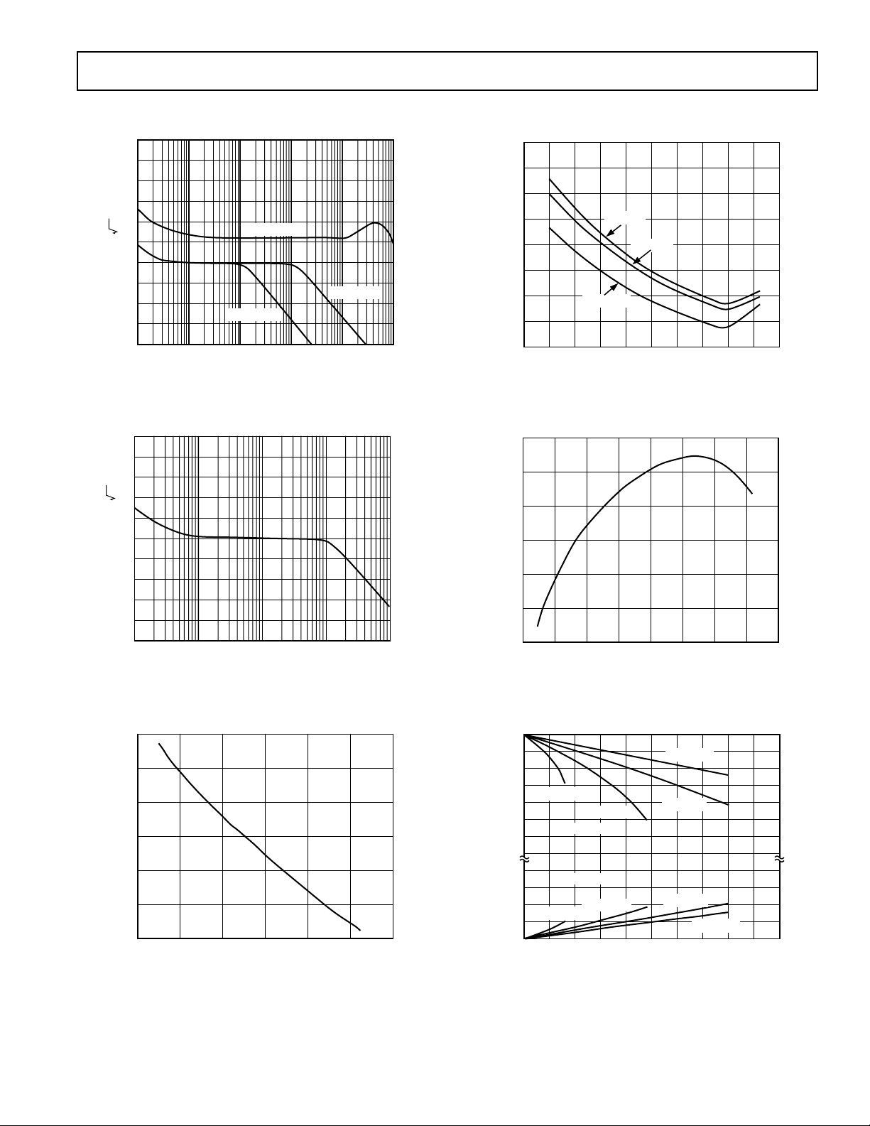
Typical Performance Characteristics
100
90
80
70
60
50
40
NOISE – nV/ Hz, RTI
30
20
10
0
1
10 100 1k 10k 100k
Figure 2. Voltage Noise Spectral Density vs. Frequency
100
90
80
70
60
50
40
30
CURRENT NOISE – fA/ Hz
20
10
0
1
10 100 1k 10k
Figure 3. Current Noise Spectral Density vs. Frequency
GAIN = 5
GAIN = 100
GAIN = 1000
FREQUENCY – Hz
FREQUENCY – Hz
(@ +25ⴗC VS = ⴞ5 V, RL = 20 k⍀ unless otherwise noted)
–5.5
–5.0
–4.5
–4.0
–3.5
–3.0
–2.5
INPUT BIAS CURRENT – nA
–2.0
–1.5
–60 140–40
Figure 5. Input Bias Current vs. Temperature
65.5
64.5
63.5
62.5
61.5
POWER SUPPLY CURRENT – mA
60.5
59.5
0
TOTAL POWER SUPPLY VOLTAGE – Volts
Figure 6. Supply Current vs. Supply Voltage
VS = +5V
VS = 65V
VS = 615V
0
–20
20 40 60 80 100 120
TEMPERATURE – 8C
10 15 20 25 30 35
405
–3.200
–3.000
–2.800
–2.600
–2.400
INPUT BIAS CURRENT – nA
–2.200
–2.000
–15 15–10
COMMON-MODE INPUT – Volts
Figure 4. I
–5
BIAS
0
510
vs. CMV, VS = ±15 V
Figure 7. Output Voltage Swing vs. Output Current
–5–REV. A
Page 6

AD627
G = 1000
G = 100
G = 5
FREQUENCY – Hz
120
PSRR – dB
110
100
90
80
70
60
50
40
30
20
10 100 1k 10k 100k
G = 1000
G = 100
G = 5
FREQUENCY – Hz
120
PSRR – dB
110
100
90
80
70
60
50
40
30
20
10 100 1k 10k 100k
500mV
100
90
10
0%
1s
Figure 8. 0.1 Hz to 10 Hz Current Noise (0.71 pA/DIV)
20mV
100
90
10
0%
1s
Figure 9. 0.1 Hz to 10 Hz RTI Voltage Noise (400 nV/DIV),
G = 5
Figure 11. Positive PSRR vs. Frequency, ±5 V
100
90
80
70
60
50
PSRR – dB
40
30
20
10
0
10 100 1k 10k 100k
FREQUENCY – Hz
G = 1000
G = 100
G = 5
Figure 12. Negative PSRR vs. Frequency, ±5 V
2V
100
90
10
0%
Figure 10. 0.1 Hz to 10 Hz RTI Voltage Noise (200 nV/DIV),
G = 1000
1s
Figure 13. Positive PSRR vs. Frequency (VS = +5 V, 0 V)
–6– REV. A
Page 7

10
OUTPUT PULSE – Volts
400
200
0
0
610
SETTLING TIME – ms
62 64 66 68
300
100
1
SETTLING TIME – ms
AD627
0.1
51k
10010
GAIN – V/V
Figure 14. Settling Time to 0.01% vs. Gain for a 5 V Step
at Output, R
= 20 kΩ, CL = 100 pF, VS = ±5 V
L
Figure 15. Large Signal Pulse Response and Settling
Time, G = –5, R
= 20 kΩ, CL = 100 pF (1.5 mV = 0.01%)
L
Figure 17. Settling Time to 0.01% vs. Output Swing,
G = 5, R
= 20 kΩ, CL = 100 pF
L
Figure 18. Large Signal Pulse Response and Settling
Time, G = –100, R
= 20 kΩ, CL = 100 pF (100 µV = 0.01%)
L
Figure 16. Large Signal Pulse Response and Settling
Time, G = –10, R
= 20 kΩ, CL = 100 pF (1.0 mV = 0.01%)
L
Figure 19. Large Signal Pulse Response and Settling
Time, G = –1000, R
= 20 kΩ, CL = 100 pF (10 µV = 0.01%)
L
–7–REV. A
Page 8

AD627
120
110
100
90
80
70
60
50
CMRR – dB
40
30
20
10
0
1 10 1k 10k 100k
100
FREQUENCY – Hz
Figure 20. CMRR vs. Frequency, ±5 VS, (CMV = 200 mV p-p)
70
G = 1000
G = 100
G = 10
G = 5
100 1k 10k 100k
FREQUENCY – Hz
60
50
40
30
20
GAIN – dB
10
0
–10
–20
–30
Figure 21. Gain vs. Frequency (VS = +5 V, 0 V), V
G = 5
G = 1000
G = 100
= 2.5 V
REF
Figure 23. Small Signal Pulse Response, G = +10,
R
= 20 kΩ, CL = 50 pF
L
Figure 24. Small Signal Pulse Response, G = +100,
R
= 20 kΩ, CL = 50 pF
L
Figure 22. Small Signal Pulse Response, G = +5,
R
= 20 kΩ, CL = 50 pF
L
Figure 25. Small Signal Pulse Response,
G = +1000, R
= 20 kΩ, CL = 50 pF
L
–8– REV. A
Page 9

20mV/DIV
V
OUT
3V/DIV
200
m
V/DIV
V
OUT
3V/DIV
200
m
V/DIV
V
OUT
3V/DIV
200
m
V/DIV
V
OUT
0.5V/DIV
AD627
Figure 26. Gain Nonlinearity, VS = ±2.5 V, G = 5
(4 ppm/DIV)
m
V/DIV
40
V
OUT
0.5V/DIV
Figure 27. Gain Nonlinearity, VS = ±2.5 V, G = 100
(8 ppm/DIV)
40
m
V/DIV
Figure 29. Gain Nonlinearity, VS = ±15 V, G = 100
(7 ppm/DIV)
Figure 30. Gain Nonlinearity, VS = ±15 V, G = +5 (7 ppm/DIV)
Figure 28. Gain Nonlinearity, VS = ±15 V, G = 5
(1.5 ppm/DIV)
V
OUT
3V/DIV
Figure 31. Gain Nonlinearity, VS = ±15 V, G = +100 (7 ppm/DIV)
–9–REV. A
Page 10

AD627
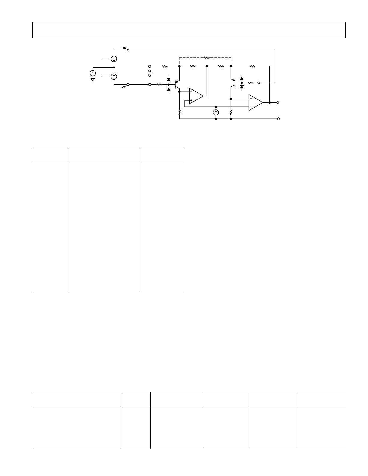
THEORY OF OPERATION
The AD627 is a true “instrumentation amplifier” built using
two feedback loops. Its general properties are similar to those of
the classic “two op amp” instrumentation amplifier configuration, and can be regarded as such, but internally the details are
somewhat different. The AD627 uses a modified “current feedback” scheme which, coupled with interstage feedforward
frequency compensation, results in a much better CMRR
(Common-Mode Rejection Ratio) at frequencies above dc (notably the line frequency of 50 Hz–60 Hz) than might otherwise
be expected of a low power instrumentation amplifier.
Referring to the diagram, (Figure 32), A1 completes a feedback
loop which, in conjunction with V1 and R5, forces a constant
collector current in Q1. Assume that the gain-setting resistor
) is not present for the moment. Resistors R2 and R1 com-
(R
G
plete the loop and force the output of A1 to be equal to the
voltage on the inverting terminal with a gain of (almost exactly)
1.25. A nearly identical feedback loop completed by A2 forces a
current in Q2 which is substantially identical to that in Q1, and
A2 also provides the output voltage. When both loops are balanced, the gain from the noninverting terminal to V
to 5, whereas the gain from the output of A1 to V
is equal
OUT
is equal to
OUT
–4. The inverting terminal gain of A1, (1.25) times the gain of
A2, (–4) makes the gain from the inverting and noninverting
terminals equal.
EXTERNAL GAIN RESISTOR
REF
–IN
100kV
2kV
R1
+V
S
Q1
–V
S
R5
200kV
R2
25kV
A1
R
G
R3
25kV
Q2
V1
+V
–V
R6
200kV
100kV
S
S
R4
2kV
+IN
A2
OUTPUT
–V
S
Figure 32. Simplified Schematic
The differential mode gain is equal to 1 + R4/R3, nominally five
and is factory trimmed to 0.01% final accuracy. Adding an external
gain setting resistor (R
to (R4 + R1)/R
G
) increases the gain by an amount equal
G
. The output voltage of the AD627 is given by the
following equation.
V
= [VIN(+) – V
OUT
(–)] × (5 + 200 kΩ/R
IN
) + V
G
REF
Laser trims are performed on R1 through R4 to ensure that
their values are as close as possible to the absolute values in the
gain equation. This ensures low gain error and high commonmode rejection at all practical gains.
USING THE AD627
Basic Connections
Figure 33 shows the basic connection circuit for the AD627.
The +V
The supply can either be bipolar (V
single supply (–V
and –VS terminals are connected to the power supply.
S
= 0 V, +V
S
= ±1.1 V to ±18 V) or
S
= +2.2 V to +36 V). The power
S
supplies should be capacitively decoupled close to the devices
power pins. For best results, use surface mount 0.1 µF ceramic
chip capacitors.
The input voltage, which can be either single ended (tie either
–IN or +IN to ground) or differential. The difference between
the voltage on the inverting and noninverting pins is amplified
by the programmed gain. The programmed gain is set by the
gain resistor (see below). The output signal appears as the voltage difference between the output pin and the externally applied
voltage on the REF pin (see below).
Setting the Gain
The AD627s gain is resistor programmed by RG, or more precisely, by whatever impedance appears between Pins 1 and 8.
The gain is set according to the equation:
Gain = 5 + (200 kΩ/R
)
G
or
R
= 200 kΩ/(Gain – 5)
G
It follows that the minimum achievable gain is 5 (for R
= ∞).
G
With an internal gain accuracy of between 0.05% and 0.7%
depending on gain and grade, a 0.1% external gain resistor
would seem appropriate to prevent significant degradation of the
overall gain error. However, 0.1% resistors are not available in a
wide range of values and are quite expensive. Table I shows
recommended gain resistor values using 1% resistors. For all
gains, the size of the gain resistor is conservatively chosen as the
closest value from the standard resistor table that is higher than
the ideal value. This results in a gain that is always slightly less
than the desired gain. This prevents clipping of the signal at the
output due to resistor tolerance.
The internal resistors on the AD627 have a negative tempera-
ture coefficient of –75 ppm/°C max for gains > 5. Using a gain
resistor that also has a negative temperature coefficient of
–75 ppm/°C or less will tend to reduce the overall circuit’s gain
drift.
+V
S
+1.1V TO +18V
R
R
G
G
–V
0.1mF
OUTPUT
REF
0.1mF
–1.1V TO –18V
S
V
OUT
REF (INPUT)
GAIN = 5 + (200kV/RG)
+IN
V
IN
–IN
+IN
V
R
IN
G
–IN
+V
S
+2.2V TO +36V
0.1mF
R
G
R
G
OUTPUT
REF
R
G
V
OUT
REF (INPUT)
Figure 33. Basic Connections for Single and Dual Supplies
–10– REV. A
Page 11
V+
V
DIFF
2
V
V
CM
DIFF
2
+IN
–IN
100kV
2kV
REF
–IN
V–
EXTERNAL GAIN RESISTOR
+V
S
Q1
–V
S
A1
200kV
R
G
25kV25kV
Q2
V
A
+V
–V
200kV
100kV
S
S
2kV
+IN
A2
Figure 34. Amplifying Differential Signals with a Common-Mode Component
OUTPUT
–V
S
AD627
Table I. Recommended Values of Gain Resistors
Desired 1% Std Table Resulting
Gain Value of RG, ⍀ Gain
5
∞
5
6 200 k 6
7 100 k 7
8 68.1 k 7.93
9 51.1 k 8.91
10 40.2 k 9.98
15 20 k 15
20 13.7 k 19.6
25 10 k 25
30 8.06 k 29.81
40 5.76 k 39.72
50 4.53 k 49.15
60 3.65 k 59.79
70 3.09 k 69.73
80 2.67 k 79.9
90 2.37 k 89.39
100 2.1 k 99.24
200 1.05 k 195.48
500 412 489.44
1000 205 980.61
Reference Terminal
The reference terminal potential defines the zero output voltage
and is especially useful when the load does not share a precise
ground with the rest of the system. It provides a direct means of
injecting a precise offset to the output. The reference terminal is
also useful when bipolar signals are being amplified as it can be
used to provide a virtual ground voltage.
Since the AD627 output voltage is developed with respect to the
potential on the reference terminal, it can solve many grounding
problems by simply tying the REF pin to the appropriate “local
ground.” The REF pin should however be tied to a low impedance point for optimal CMR.
Input Range Limitations in Single Supply Applications
In general, the maximum achievable gain is determined by the
available output signal range. However, in single supply applications where the input common mode voltage is close to or equal
to zero, some limitations on the gain can be set. While the Input, Output and Reference Pins have ranges that are nominally
defined on the specification pages, there is a mutual interdependence between the voltage ranges on these pins. Figure 34 shows
the simplified schematic of the AD627, driven by a differential
voltage V
voltage on the output of op amp A1 is a function of V
which has a common mode component, VCM. The
DIFF
DIFF
, VCM,
the voltage on the REF pin and the programmed gain. This
voltage is given by the equation:
= 1.25 (VCM + 0.5 V) – 0.25 V
V
A1
REF
– V
DIFF
(25 kΩ/R
– 0.625)
G
We can also express the voltage on A1 as a function of the actual voltages on the –IN and +IN pins (V– and V+)
= 1.25 (V– + 0.5 V) – 0.25 V
V
A1
– (V+ – V–) 25 kΩ/R
REF
G
A1’s output is capable of swinging to within 50 mV of the negative rail and to within 200 mV of the positive rail. From either of
the above equations, it is clear that an increasing V
, (while it
REF
acts as a positive offset at the output of the AD627), tends to
decrease the voltage on A1. Figures 35 and 36 show the maximum voltages that can be applied to the REF pin, for a gain of
five for both the single and dual supply cases. Raising the input
common-mode voltage will increase the voltage on the output of
A1. However, in single supply applications where the commonmode voltage is low, a differential input voltage or a voltage on
REF that is too high can drive the output of A1 into the ground
rail. Some low side headroom is added by virtue of both inputs
being shifted upwards by about 0.5 V (i.e., by the V
of Q1
BE
and Q2). The above equations can be used to check that the
voltage on amplifier A1 is within its operating range.
Table II gives values for the maximum gains for various single
supply input conditions. The resulting output swings shown
refer to 0 V. The voltages on the REF pins has been set to either
Table II. Maximum Gain for Low Common-Mode Single Supply Applications
REF Supply RG (1% Resulting Output Swing
V
IN
±100 mV, V
±50 mV, V
±10 mV, V
= 0 V 2 V +5 V to +15 V 28.7 kΩ 12.0 0.8 V to 3.2 V
CM
= 0 V 2 V +5 V to +15 V 10.7 kΩ 23.7 0.8 V to 3.2 V
CM
= 0 V 2 V +5 V to +15 V 1.74 kΩ 119.9 0.8 V to 3.2 V
CM
Pin Voltage Tolerance) Max Gain WRT 0 V
V– = 0 V, V+ = 0 V to 1 V 1 V +10 V to +15 V 78.7 kΩ 7.5 1 V to 8.5 V
V– = 0 V, V+ = 0 mV to 100 mV 1 V +5 V to +15 V 7.87 kΩ 31 1 V to 4.1 V
V– = 0 V, V+ = 0 mV to 10 mV 1 V +5 V to +15 V 7.87 Ω 259.1 1 V to 3.6 V
–11–REV. A
Page 12

AD627
2 V or 1 V to maximize the available gain and output swing.
Note that in most cases, there is no advantage to increasing the
single supply to greater than 5 V (the exception being an input
range of 0 V to 1 V).
5
4
3
2
1
0
– Volts
REF
–1
V
–2
–3
–4
–5
–6
MAXIMUM V
–5 –4 –3 –2 –1
REF
VIN(–) – Volts
MINIMUM V
0
REF
1234
Figure 35. Reference Input Voltage vs. Negative Input
Voltage, V
= ±5 V, G = 5
S
5
4
3
– Volts
REF
2
V
1
0
–0.5
MAXIMUM V
0 0.5 1 1.5 2 2.5 3 3.5 4 4.5
REF
MINIMUM V
VIN(–) – Volts
REF
Figure 36. Reference Input Voltage vs. Negative Input
Voltage, V
= +5 V, G = 5
S
Output Buffering
The AD627 is designed to drive loads of 20 kΩ or greater but
can deliver up to 20 mA to heavier loads at lower output voltage
swings (see Figure 7). If more than 20 mA of output current is
required at the output, the AD627’s output should be buffered
with a precision op amp such as the OP113 as shown in Figure
37 (shown for the single supply case). This op amp can swing
from 0 V to 4 V on its output while driving a load as small as
600 Ω.
+V
S
0.1mF
0.1mF
R
V
IN
AD627
G
REF
0.1mF
–V
S
OP113
–V
0.1mF
S
V
OUT
Figure 37. Output Buffering
INPUT AND OUTPUT OFFSET ERRORS
The low errors of the AD627 are attributed to two sources,
input and output errors. The output error is divided by G when
referred to the input. In practice, the input errors dominate at
high gains and the output errors dominate at low gains. The
total offset error for a given gain is calculated as:
Total Error RTI = Input Error + (Output Error/Gain)
Total Error RTO = (Input Error
×
G) + Output Error
RTI offset errors and noise voltages for different gains are shown
below in Table III.
Table III. RTI Error Sources
Max Total Max Total
RTI Offset Error RTI Offset Drift Total RTI Noise
V V V/ⴗC V/ⴗC nV/
√
Hz
Gain AD627A AD627B AD627A AD627B AD627A & AD627B
5 450 250 5 3 95
10 350 200 4 2 66
20 300 175 3.5 1.5 56
50 270 160 3.2 1.2 53
100 270 155 3.1 1.1 52
500 252 151 3 1 52
1000 251 151 3 1 52
Make vs. Buy: A Typical Application Error Budget
The example in Figure 38 serves as a good comparison between
the errors associated with an integrated and a discrete in amp
implementation. A ±100 mV signal from a resistive bridge
(common-mode voltage = +2.5 V) is to be amplified. This example compares the resulting errors from a discrete two op
amp in amp and from the AD627. The discrete implementation
uses a four-resistor precision network (1% match, 50 ppm/°C
tracking).
The errors associated with each implementation are detailed in
Table IV and show the integrated in amp to be more precise,
both at ambient and over temperature. It should be noted that
the discrete implementation is also more expensive. This is primarily due to the relatively high cost of the low drift precision
resistor network.
Note, the input offset current of the discrete in amp implementation is the difference in the bias currents of the two op amps,
not the offset currents of the individual op amps. Also, while the
values of the resistor network are chosen so that the inverting
and noninverting inputs of each op amp see the same impedance
(about 350 Ω), the offset current of each op amp will add an
additional error which must be characterized.
Errors Due to AC CMRR
In Table IV, the error due to common-mode rejection is the
error that results from the common-mode voltage from the
bridge 2.5 V. The ac error due to nonideal common-mode
rejection cannot be calculated without knowing the size of the ac
common-mode voltage (usually interference from 50 Hz/60 Hz
mains frequencies).
A mismatch of 0.1% between the four gain setting resistors will
determine the low frequency CMRR of a two op amp in amp.
The plot in Figure 38 shows the practical results, at ambient
temperature, of resistor mismatch. The CMRR of the circuit in
Figure 39 (Gain = 11) was measured using four resistors which
–12– REV. A
Page 13

AD627
FREQUENCY – Hz
120
1
CMRR – dB
110
100
90
80
70
60
50
40
30
20
10 100 1k 10k 100k
350V
350V
+5V
350V
350V
6100mV
AD627A GAIN = 9.98
R
40.2kV
1%
+10ppm/ C
G
+5V
AD627A
(5+(200kV/R
LT1078IS8
V
OUT
2.5V
))
G
2.5V
*1% REGISTER MATCH, 50ppm/8C TRACKING
1/2
350V*3.15kV* 350V*
"HOMEBREW" IN AMP, G = 10
+5V
LT1078IS8
1/2
3.15kV*
V
OUT
Figure 38. Make vs. Buy
Table IV. Make vs. Buy Error Budget
“Homebrew” Total Error Total Error
Error Source AD627 Circuit Calculation Circuit Calculation AD627-ppm Homebrew–ppm
ABSOLUTE ACCURACY at T
Total RTI Offset Voltage, mV (250 µV + (1000 µV/10))/100 mV (180 µV × 2)/100 mV 3500 3600
Input Offset Current, nA 1 nA × 350 Ω/100 mV 20 nA × 350 Ω/100 mV 3.5 70
Internal Offset Current (Homebrew Only) Not Applicable 0.7 nA × 350 Ω/100 mV 2.45
CMRR, dB 77 dB→141 ppm × 2.5 V/100 mV (1% Match × 2.5 V)/10/100 mV 3531 25000
Gain 0.35% + 0.1% 1% Match 13500 10000
DRIFT TO +85°C
Gain Drift, ppm/°C (–75 + 10) ppm/°C × 60°C 50 ppm/°C × 60°C 3900 3000
Total RTI Offset Voltage, mV/°C (3.0 µV/°C + (10 µV/°C/10)) (2 × 3.5 µV/°C × 60°C)/100 mV
Input Offset Current, pA/°C (16 pA/°C × 350 Ω × 60°C)/100 mV (33 pA/°C × 350 Ω × 60°C)/100 mV 3.5 7
= +25°C
A
Total Absolute Error 20535 38672
× 60°C/100 mV 2600 4200
Total Drift Error 6504 7207
Grand Total Error 27039 45879
had a mismatch of almost exactly 0.1% (R1 = 9999.5 Ω, R2 =
999.76 Ω, R3 = 1000.2 Ω, R4 = 9997.7 Ω). As expected the
CMRR at dc was measured at about 84 dB (calculated value
is 85 dB). However, as the frequency increases, the CMRR
quickly degrades. For example, a 200 mV peak-peak harmonic
of the mains frequency at 180 Hz would result in an output
voltage of about 800 µV. To put this in context, a 12-bit data
acquisition system with an input range of 0 V to 2.5 V, has an
LSB weighting of 610 µV.
By contrast, the AD627 uses precision laser trimming of internal
resistors along with patented CMR trimming to yield a higher
dc CMRR and a wider bandwidth over which the CMRR is flat
(see Figure 20).
+5V
VIN–
VIN+
R1
9999.5V
1/2
AD296
–5V
R2
999.76V
A1
R3
1000.2V
1/2
AD296
R4
9997.7V
A2
V
OUT
Figure 39. 0.1% Resistor Mismatch Example
–13–REV. A
Figure 40. CMRR Over Frequency of Discrete In Amp in
Figure 39
Ground Returns for Input Bias Currents
Input bias currents are those dc currents that must flow in
order to bias the input transistors of an amplifier. These are
usually transistor base currents. When amplifying “floating”
input sources such as transformers, or ac-coupled sources,
there must be a direct dc path into each input in order that the
bias current can flow. Figure 41 shows how a bias current
path can be provided for the case of transformer coupling,
capacitive ac-coupling and for a thermocouple application.
Page 14

AD627
In dc-coupled resistive bridge applications, providing this path
is generally not necessary as the bias current simply flows from
the bridge supply, through the bridge and into the amplifier.
However, if the impedance that the two inputs see are large, and
differ by a large amount (>10 kΩ), the offset current of the
input stage will cause dc errors compatible with the input offset
voltage of the amplifier.
+V
AD627
–V
S
S
REFERENCE
LOAD
V
OUT
TO POWER
SUPPLY
GROUND
–INPUT
+INPUT
R
G
Figure 41a. Ground Returns for Bias Currents with Transformer Coupled Inputs
+V
AD627
–V
S
S
REFERENCE
LOAD
V
OUT
TO POWER
SUPPLY
GROUND
–INPUT
+INPUT
R
G
Figure 41b. Ground Returns for Bias Currents with Thermocouple Inputs
+V
AD627
–V
S
S
REFERENCE
LOAD
V
OUT
TO POWER
SUPPLY
GROUND
–INPUT
+INPUT
100kV 100kV
R
G
Figure 41c. Ground Returns for Bias Currents with AC
Coupled Inputs
Layout and Grounding
The use of ground planes is recommended to minimize the
impedance of ground returns (and hence the size of dc errors).
In order to isolate low level analog signals from a noisy digital
environment, many data-acquisition components have separate
analog and digital ground returns (Figure 42). All ground pins
from mixed signal components such as analog-to-digital converters
should be returned through the “high quality” analog ground
plane. Digital ground lines of mixed signal components should
also be returned through the analog ground plane. This may
seem to break the rule of keeping analog and digital grounds
separate. However, in general, there is also a requirement to
keep the voltage difference between digital and analog grounds
on a converter as small as possible (typically <0.3 V). The
increased noise, caused by the converter’s digital return currents
flowing through the analog ground plane, will generally be negligible. Maximum isolation between analog and digital is achieved
by connecting the ground planes back at the supplies.
If there is only a single power supply available, it must be shared
by both digital and analog circuitry. Figure 43 shows the how to
minimize interference between the digital and analog circuitry.
As in the previous case, separate analog and digital ground
planes should be used (reasonably thick traces can be used as an
alternative to a digital ground plane). These ground planes
should be connected at the power supply’s ground pin. Separate
traces (or power planes) should be run from the power supply to
the supply pins of the digital and analog circuits. Ideally each
device should have its own power supply trace, but these can be
shared by a number of devices as long as a single trace is not
used to route current to both digital and analog circuitry.
INPUT PROTECTION
As shown in the simplified schematic (Figure 32), both the
inverting and noninverting inputs are clamped to the positive
and negative supplies by ESD diodes. In addition to this a 2 kΩ
series resistor on each input provides current limiting in the
event of an overvoltage. These ESD diodes can tolerate a maximum continuous current of 10 mA. So an overvoltage, (that is
the amount by which input voltage exceeds the supply voltage),
of ±20 V can be tolerated. This is true for all gains, and for
power on and off. This last case is particularly important since
the signal source and amplifier may be powered separately.
If the overvoltage is expected to exceed 20 V, additional external
series resistors current limiting resistors should be used to keep
the diode current to below 10 mA.
0.1mF
AD627
ANALOG POWER SUPPLY
+5V –5V
0.1mF
V
IN1
V
IN2
GND
0.1mF
VDDAGND DGND
ADC
AD7892-2
DIGITAL POWER SUPPLY
12
+5V
GND
0.1mF
AGND V
DD
mPROCESSOR
Figure 42. Optimal Grounding Practice for a Bipolar Supply Environment with Separate Analog and Digital Supplies
–14– REV. A
Page 15

AD627
AD627
V
OUT
+V
S
V
DIFF
RG =
200kV
GAIN-5
–V
S
V
REF
0.1mF
0.1mF
0.1mF
AD627
V
IN
Figure 43. Optimal Ground Practice in a Single Supply Environment
RF INTERFERENCE
All instrumentation amplifiers can rectify high frequency out-ofband signals. Once rectified, these signals appear as dc offset
errors at the output. The circuit of Figure 44 provides good RFI
suppression without reducing performance within the in amp’s
passband. Resistor R1 and capacitor C1 (and likewise, R2 and
C2) form a low pass RC filter that has a –3 dB BW equal to:
F = 1/(2 π R1C1). Using the component values shown, this
filter has a –3 dB bandwidth of approximately 8 kHz. Resistors
R1 and R2 were selected to be large enough to isolate the circuit’s
input from the capacitors, but not large enough to significantly
increase the circuit’s noise. To preserve common-mode rejection in the amplifier’s pass band, capacitors C1 and C2 need to
be 5% mica units, or low cost 20% units can be tested and
“binned” to provide closely matched devices.
+V
S
AD627
–V
S
0.01mF
REFERENCE
0.01mF
V
OUT
1000pF
5%
0.022mF
1000pF
5%
C1
C3
C2
R1
20kV
1%
+IN
R2
20kV
1%
–IN
LOCATE C1–C3 AS CLOSE TO
THE INPUT PINS AS POSSIBLE
R
G
0.33mF
0.33mF
Figure 44. Circuit to Attenuate RF Interference
Capacitor C3 is needed to maintain common-mode rejection at
the low frequencies. R1/R2 and C1/C2 form a bridge circuit
whose output appears across the in amp’s input pins. Any mismatch between C1 and C2 will unbalance the bridge and reduce
common-mode rejection. C3 insures that any RF signals are
common mode (the same on both in amp inputs) and are not
applied differentially. This second low pass network, R1 + R2
and C3, has a –3 dB frequency equal to: 1/(2 π (R1 + R2) (C3)).
Using a C3 value of 0.022 µF as shown, the –3 dB signal BW of
this circuit is approximately 200 Hz. The typical dc offset shift
over frequency will be less than 1 mV and the circuit’s RF signal
rejection will be better than 57 dB. The 3 dB signal bandwidth
POWER SUPPLY
+5V
V
GND
0.1mF
0.1mF
12
V
mPROCESSOR
DGND
AGND
DD
ADC
AD7892-2
DGND
DD
of this circuit may be increased by reducing the value of resistors
R1 and R2. The performance is similar to that using 20 kΩ
resistors, except that the circuitry preceding the in amp must
drive a lower impedance load.
The circuit of Figure 44 should be built using a PC board with a
ground plane on both sides. All component leads should be as
short as possible. Resistors R1 and R2 can be common 1%
metal film units but capacitors C1 and C2 need to be ±5%
tolerance devices to avoid degrading the circuit’s commonmode rejection. Either the traditional 5% silver mica units or
Panasonic ±2% PPS film capacitors are recommended.
APPLICATIONS CIRCUITS
A Classic Bridge Circuit
Figure 45 shows the AD627 configured to amplify the signal
from a classic resistive bridge. This circuit will work in either
dual or single supply mode. Typically the bridge will be excited
by the same voltage as is used to power the in amp. Connecting
the bottom of the bridge to the negative supply of the in amp (usually either 0, –5 V, –12 V or –15 V), sets up an input common
mode voltage that is optimally located midway between the
supply voltages. It is also appropriate to set the voltage on the
REF pin to midway between the supplies, especially if the input
signal will be bipolar. However the voltage on the REF pin can
be varied to suit the application. A good example of this is when
the REF pin is tied to the V
Converter (ADC) whose input range is (V
available output swing on the AD627 of (–V
– 150 mV) the maximum programmable gain is simply this
(+V
S
pin of an Analog-to-Digital
REF
± V
REF
). With an
IN
+ 100 mV) to
S
output range divided by the input range.
Figure 45. A Classic Bridge Circuit
–15–REV. A
Page 16

AD627
R
G
2.1kV
AD627
0.1mF
V
OUT
+5V
J-TYPE
THERMOCOUPLE
2V
REF
0.0098 (0.25)
0.0075 (0.19)
0.0500 (1.27)
0.0160 (0.41)
88
08
0.0196 (0.50)
0.0099 (0.25)
3 458
85
41
0.1 968 (5.00)
0.1 890 (4.80)
0.2440 (6.20)
0.2284 (5.80)
PIN 1
0.1574 (4.00)
0.1497 (3.80)
0.0500 (1.27)
BSC
0.0688 (1.75)
0.0532 (1.35)
SEATING
PLANE
0.0098 (0.25)
0.0040 (0.10)
0.0192 (0.49)
0.0138 (0.35)
4–20mA
TRANSDUCER
MicroConverter is a trademark of Analog Devices, Inc.
LINE
IMPEDANCE
4–20mA
24.9V
Figure 46. A 4 mA-to-20 mA Receiver Circuit
A 4 mA-to-20 mA Single Supply Receiver
Figure 46 shows how a signal from a 4 mA-to-20 mA transducer
can be interfaced to the ADµC812, a 12-bit ADC with an em-
bedded microcontroller. The signal from a 4 mA-to-20 mA
transducer is single ended. This initially suggests the need for
a simple shunt resistor, to convert the current to a voltage at the
high impedance analog input of the converter. However, any
line resistance in the return path (to the transducer) will add a
current dependent offset error. So the current must be sensed
differentially.
In this example, a 24.9 Ω shunt resistor generates a maximum
differential input voltage to the AD627 of between 100 mV (for
4 mA in) and 500 mV (for 20 mA in). With no gain resistor
present, the AD627 amplifies the 500 mV input voltage by a
factor of 5, to 2.5 V, the full-scale input voltage of the ADC.
The zero current of 4 mA corresponds to a code of 819 and the
LSB size is 4.9 mA.
A Thermocouple Amplifier
Because the common-mode input range of the AD627 extends
0.1 V below ground, it is possible to measure small differential
signals which have low, or no, common mode component. Figure 47 shows a thermocouple application where one side of the
J-type thermocouple is grounded.
G = 5
+5V
AD627
0.1mF
REF
V
REF
AIN 0–7
+5V
AVDD
AGND DGND
+5V
0.1mF 0.1mF
DVDD
ADmC812
MicroConverter
TM
Over a temperature range from –200°C to +200°C, the J-type
thermocouple delivers a voltage ranging from –7.890 mV to
10.777 mV. A programmed gain on the AD627 of 100 (R
=
G
2.1 kΩ) and a voltage on the AD627 REF pin of 2 V, results in
the AD627’s output voltage ranging from 1.110 V to 3.077 V
relative to ground. For a different input range or different voltage on the REF pin, it is important to check that the voltage on
internal node A1 (see Figure 34) is not driven below ground).
This can be checked using the equations in the section entitled
Input Range Limitations in Single Supply Applications.
Figure 47. Amplifying Bipolar Signals with Low CommonMode Voltage
C3430a–0–12/99 (rev. A)
PIN 1
0.210 (5.33)
MAX
0.160 (4.06)
0.115 (2.93)
0.022 (0.558)
0.014 (0.356)
8-Lead Plastic DIP
0.430 (10.92)
0.348 (8.84)
8
5
0.280 (7.11)
14
0.100
(2.54)
BSC
0.240 (6.10)
0.060 (1.52)
0.015 (0.38)
0.070 (1.77)
0.045 (1.15)
(N-8)
0.130
(3.30)
MIN
SEATING
PLANE
0.325 (8.25)
0.300 (7.62)
0.015 (0.381)
0.008 (0.204)
OUTLINE DIMENSIONS
Dimensions shown in inches and (mm).
0.195 (4.95)
0.115 (2.93)
–16–
8-Lead SOIC
(SO-8)
PRINTED IN U.S.A.
REV. A
 Loading...