

Page 1
1
2
3
4
8
7
6
5
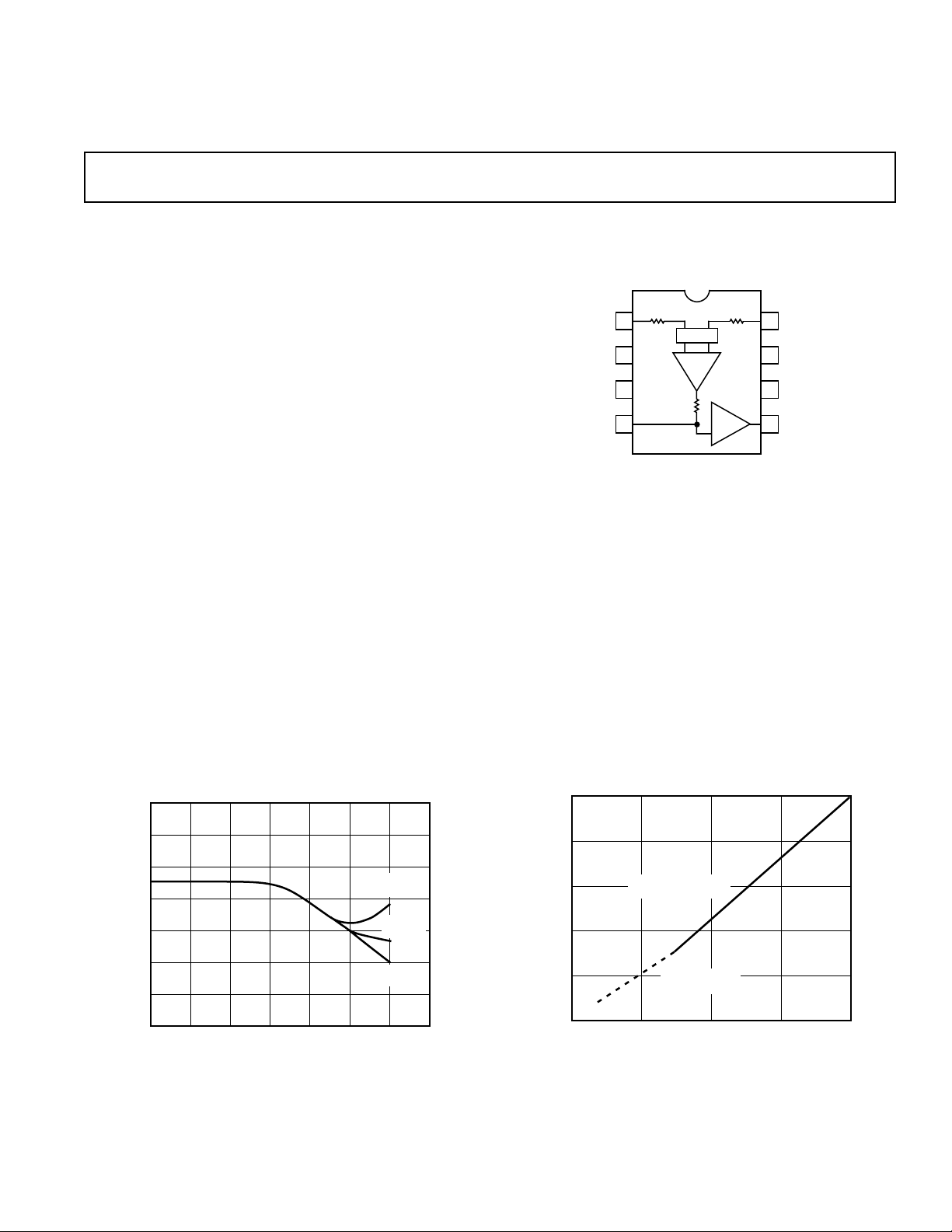
AD626
1/6
200kV
–IN
ANALOG
GND
–V
S
FILTER
+IN
G = 100
OUT
+V
S
100kV
G
=
2
G = 30
200kV
Low Cost, Single Supply
25
0
5
15
5
2
10
1
20
4
3
POWER SUPPLY VOLTAGE – 6Volts
INPUT COMMON MODE RANGE – Volts
6VCM FOR SINGLE
AND DUAL SUPPLIES
6VCM FOR DUAL
SUPPLIES ONLY
a
FEATURES
Pin Selectable Gains of 10 and 100
True Single Supply Operation
Single Supply Range of +2.4 V to +10 V
Dual Supply Range of ⴞ1.2 V to ⴞ6 V
Wide Output Voltage Range of 30 mV to 4.7 V
Optional Low-Pass Filtering
Excellent DC Performance
Low Input Offset Voltage: 500 V max
Large Common-Mode Range: 0 V to +54 V
Low Power: 1.2 mW (V
Good CMR of 90 dB typ
AC Performance
Fast Settling Time: 24 s (0.01%)
Includes Input Protection
Series Resistive Inputs (R
RFI Filters Included
Allows 50 V Continuous Overload
APPLICATIONS
Current Sensing
Interface for Pressure Transducers, Position Indicators,
Strain Gages, and Other Low Level Signal Sources
PRODUCT DESCRIPTION
The AD626 is a low cost, true single supply differential amplifier designed for amplifying and low-pass filtering small differential voltages from sources having a large common-mode voltage.
The AD626 can operate from either a single supply of +2.4 V to
+10 V, or dual supplies of ±1.2 V to ±6 V. The input common-
mode range of this amplifier is equal to 6 (+V
provides a +24 V CMR while operating from a +5 V supply.
Furthermore, the AD626 features a CMR of 90 dB typ.
= +5 V)
S
= 200 k⍀)
IN
– 1 V) which
S
Differential Amplifier
AD626
CONNECTION DIAGRAM
8-Lead Plastic Mini-DIP (N)
and SOIC (SO) Packages
The amplifier’s inputs are protected against continuous overload
of up to 50 V, and RFI filters are included in the attenuator
network. The output range is +0.03 V to +4.9 V using a +5 V
supply. The amplifier provides a preset gain of 10, but gains between 10 to 100 can be easily configured with an external resistor. Furthermore, a gain of 100 is available by connecting the G
= 100 pin to analog ground. The AD626 also offers low-pass
filter capability by connecting a capacitor between the filter pin
and analog ground.
The AD626A and AD626B operate over the industrial tempera-
ture range of –40°C to +85°C. The AD626 is available in two
8-lead packages: a plastic mini-DIP and SOIC.
160
140
100
80
60
CMRR – dB
REV. C
Information furnished by Analog Devices is believed to be accurate and
reliable. However, no responsibility is assumed by Analog Devices for its
use, nor for any infringements of patents or other rights of third parties
which may result from its use. No license is granted by implication or
otherwise under any patent or patent rights of Analog Devices.
40
20
0
0.1
Common-Mode Rejection vs. Frequency
G = 10,100
V
= +5V
S
G = 100
V
= 65V
S
G = 10
V
= 65V
S
1
FREQUENCY – Hz
1M
100k10k1k10010
Input Common-Mode Range vs. Supply
One Technology Way, P.O. Box 9106, Norwood, MA 02062-9106, U.S.A.
Tel: 781/329-4700 World Wide Web Site: http://www.analog.com
Fax: 781/326-8703 © Analog Devices, Inc., 1999
Page 2

AD626–SPECIFICATIONS
SINGLE SUPPLY
Model AD626A AD626B
Parameter Condition Min Typ Max Min Typ Max Units
GAIN
Gain Accuracy Total Error
Gain = 10 @ V
Gain = 100 @ V
Over Temperature, T
Gain Linearity
Gain = 10 @ V
Gain = 100 @ V
OFFSET VOLTAGE
Input Offset Voltage 1.9 2.5 1.9 2.5 mV
vs. Temperature T
vs. Temperature T
vs. Supply Voltage (PSR)
+PSR 74 80 74 80 dB
–PSR 64 66 64 66 dB
COMMON-MODE REJECTION R
+CMR Gain = 10, 100 f = 100 Hz, V
±CMR Gain = 10, 100 f = 10 kHz, V
–CMR Gain = 10, 100
COMMON-MODE VOLTAGE RANGE
+CMV Gain = 10 CMR > 85 dB +24 +24 V
–CMV Gain = 10 CMR > 85 dB –2 –2 V
INPUT
Input Resistance
Differential 200 200 kΩ
Common Mode 100 100 kΩ
Input Voltage Range (Common Mode) 6 (VS – l) 6 (VS – l) V
OUTPUT
Output Voltage Swing R
Positive Gain = 10 4.7 4.90 4.7 4.90 V
Negative Gain = 10 0.03 0.03 V
Short Circuit Current
+I
SC
NOISE
Voltage Noise RTI
Gain = 10 f = 0.1 Hz–10 Hz 2 2 µV p-p
Gain = 100 f = 0.1 Hz–10 Hz 2 2 µV p-p
Gain = 10 f = 1 kHz 0.25 0.25 µV/√Hz
Gain = 100 f = 1 kHz 0.25 0.25 µV/√Hz
DYNAMIC RESPONSE
–3 dB Bandwidth V
Slew Rate, T
Settling Time to 0.01%, 1 V Step 24 22 µs
POWER SUPPLY
Operating Range T
Quiescent Current Gain = 10 0.16 0.20 0.16 0.20 mA
TRANSISTOR COUNT # of Transistors
NOTES
1
At temperatures above +25°C, –CMV degrades at the rate of 12 mV/ °C; i.e., @ +25°C CMV = –2 V, @ +85°C CMV = –1.28 V.
Specifications subject to change without notice.
MIN
(@ +VS = +5 V and TA = +25ⴗC)
= T
A
MIN–TMAX
1
to T
MAX
≥ 100 mV dc 0.4 1.0 0.2 0.6 %
OUT
≥ 100 mV dc 0.1 1.0 0.5 0.6 %
OUT
G = 10 50 30 ppm/°C
G = 100 150 120 ppm/°C
≥ 100 mV dc 0.014 0.016 0.014 0.016 %
OUT
≥ 100 mV dc 0.014 0.02 0.014 0.02 %
OUT
MIN–TMAX
MIN–TMAX
= 10 kΩ
L
, G = 10 or 100 2.9 2.9 mV
, G = 10 or 100 6 6 µV/°C
= +24 V 66 90 80 90 dB
CM
= 6 V 55 64 55 64 dB
CM
f = 100 Hz, VCM = –2 V 60 85 73 85 dB
= 10 kΩ
L
Gain = 100 4.7 4.90 4.7 4.90 V
Gain = 100 0.03 0.03 V
12 12 mA
= +1 V dc 100 100 kHz
OUT
Gain = 10 0.17 0.22 0.17 0.22 V/µs
Gain = 100 0.1 0.17 0.1 0.17 V/µs
= T
A
MIN–TMAX
2.4 5 12 2.4 5 10 V
Gain = 100 0.23 0.29 0.23 0.29 mA
46 46
–2–
REV. C
Page 3
DUAL SUPPLY
Model AD626A AD626B
Parameter Condition Min Typ Max Min Typ Max Units
GAIN
Gain Accuracy Total Error
Gain = 10 R
Gain = 100 0.25 1.0 0.15 0.6 %
Over Temperature, T
Gain Linearity
Gain = 10 0.045 0.055 0.045 0.055 %
Gain = 100 0.01 0.015 0.01 0.015 %
OFFSET VOLTAGE
Input Offset Voltage 50 500 50 250 µV
vs. Temperature T
vs. Temperature T
vs. Supply Voltage (PSR)
+PSR 74 80 74 80 dB
–PSR 64 66 64 66 dB
COMMON-MODE REJECTION R
±CMR Gain = 10, 100 f = 100 Hz, V
±CMR Gain = 10, 100 f = 10 kHz, V
COMMON-MODE VOLTAGE RANGE
+CMV Gain = 10 CMR > 85 dB 26.5 26.5 V
–CMV Gain = 10 CMR > 85 dB 32.5 32.5 V
INPUT
Input Resistance
Differential 200 200 kΩ
Common Mode 110 110 kΩ
Input Voltage Range (Common Mode) 6 (VS – 1) 6 (VS – 1) V
OUTPUT
Output Voltage Swing R
Positive Gain = 10, 100 4.7 4.90 4.7 4.90 V
Negative Gain = 10 1.65 2.1 1.65 2.1 V
Short Circuit Current
+I
SC
–I
SC
NOISE
Voltage Noise RTI
Gain = 10 f = 0.1 Hz–10 Hz 2 2 µV p-p
Gain = 100 f = 0.1 Hz–10 Hz 2 2 µV p-p
Gain = 10 f = 1 kHz 0.25 0.25 µV/√Hz
Gain = 100 f = 1 kHz 0.25 0.25 µV/√Hz
DYNAMIC RESPONSE
–3 dB Bandwidth V
Slew Rate, T
Settling Time to 0.01%, 1 V Step 24 22 µs
POWER SUPPLY
Operating Range T
Quiescent Current Gain = 10 1.5 2 1.5 2 mA
TRANSISTOR COUNT # of Transistors
Specifications subject to change without notice.
(@ +VS = ⴞ5 V and TA = +25ⴗC)
= T
A
MIN–TMAX
to T
MIN
MAX
= 10 kΩ 0.2 0.5 0.1 0.3 %
L
G = 10 50 30 ppm/°C
G = 100 100 80 ppm/°C
MIN–TMAX
MIN–TMAX
= 10 kΩ
L
= 10 kΩ
L
, G = 10 or 100 1.0 0.5 mV
, G = 10 or 100 1.0 0.5 µV/°C
= +24 V 66 90 80 90 dB
CM
= 6 V 55 60 55 60 dB
CM
Gain = 100 1.45 1.8 1.45 1.8 V
12 12 mA
0.5 0.5 mA
= +1 V dc 100 100 kHz
OUT
Gain = 10 0.17 0.22 0.17 0.22 V/µs
Gain = 100 0.1 0.17 0.1 0.17 V/µs
= T
A
MIN–TMAX
±1.2 ±5 ±6 ±1.2 ±5 ±6V
Gain = 100 1.5 2 1.5 2 mA
46 46
AD626
REV. C –3–
Page 4
AD626
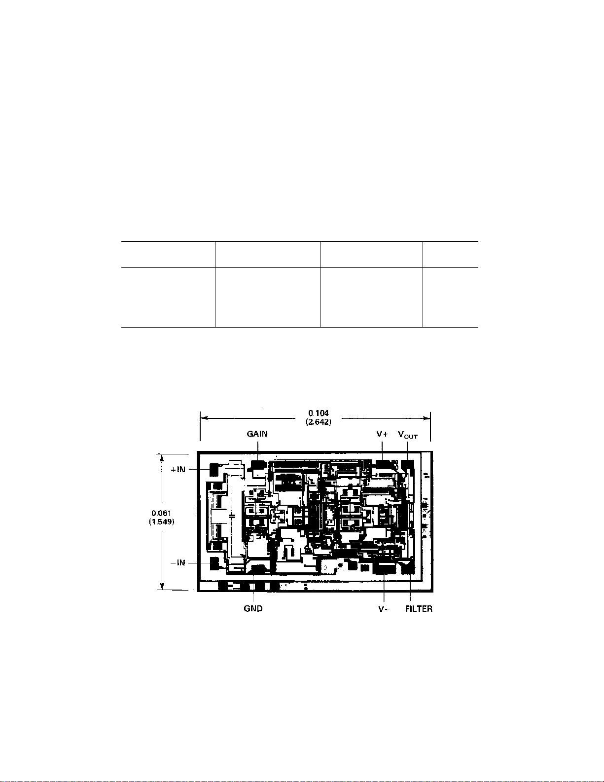
ABSOLUTE MAXIMUM RATINGS
Supply Voltage . . . . . . . . . . . . . . . . . . . . . . . . . . . . . . . . .+36 V
Internal Power Dissipation
2
1
Peak Input Voltage . . . . . . . . . . . . . . . . . . . . . . . . . . . . . . 60 V
Maximum Reversed Supply Voltage Limit . . . . . . . . . . . . –34 V
Output Short Circuit Duration . . . . . . . . . . . . . . . . . Indefinite
Storage Temperature Range (N, R) . . . . . . . . –65°C to +125°C
Operating Temperature Range
AD626A/B . . . . . . . . . . . . . . . . . . . . . . . . . –40°C to +85°C
Lead Temperature Range (Soldering 60 sec) . . . . . . . . +300°C
ORDERING GUIDE
Temperature Package Package
Model Range Descriptions Options
AD626AN –40°C to +85°C Plastic DIP N-8
AD626AR – 40°C to +85°C Small Outline IC SO-8
AD626BN –40°C to +85°C Plastic DIP N-8
AD626AR-REEL –40°C to +85°C 13" Tape and Reel
AD626AR-REEL7 –40°C to +85°C 7" Tape and Reel
NOTES
1
Stresses above those listed under Absolute Maximum Ratings may cause permanent
damage to the device. This is a stress rating only; functional operation of the device
at these or any other conditions above those indicated in the operational section of
this specification is not implied. Exposure to absolute maximum rating conditions
for extended periods may affect device reliability.
2
8-Lead Plastic Package: θJA = 100°C/W, θJC = 50°C/W.
8-Lead SOIC Package: θJA = 155°C/W, θJC = 40°C/W.
ESD SUSCEPTIBILITY
An ESD classification per method 3015.6 of MIL STD 883C
has been performed on the AD626, which is a Class 1 device.
METALIZATION PHOTOGRAPH
Dimensions shown in inches and (mm).
REV. C–4–
Page 5

6
1
–1
10 100 10k1k
4
0
2
3
5
LOAD RESISTANCE – V
POSITIVE OUTPUT VOLTAGE – Volts
VS = 65V
GAIN = 10, 100
–6
–1
1
100 1k 100k10k
–4
0
–2
–3
–5
LOAD RESISTANCE – V
NEGATIVE OUTPUT VOLTAGE – Volts
GAIN = 10
GAIN = 100
Typical Performance Characteristics–AD626
25
20
15
10
5
INPUT COMMON MODE RANGE – Volts
0
1
6VCM FOR SINGLE
AND DUAL SUPPLIES
6VCM FOR DUAL
SUPPLIES ONLY
2
SUPPLY VOLTAGE – 6Volts
3
4
5
Figure 1. Input Common-Mode Range vs. Supply
5
TA = +258C
4
SINGLE AND
DUAL SUPPLY
3
2
DUAL SUPPLY
1
ONLY
Figure 4. Positive Output Voltage Swing vs. Resistive Load
POSITIVE OUTPUT VOLTAGE SWING – Volts
0
0
1
SUPPLY VOLTAGE – Volts
432
Figure 2. Positive Output Voltage Swing vs. Supply Voltage
–5
TA = +258C
–4
–3
–2
–1
NEGATIVE OUTPUT VOLTAGE SWING – Volts
0
0
1
DUAL SUPPLY
ONLY
SUPPLY VOLTAGE – Volts
432
Figure 3. Negative Output Voltage Swing vs. Supply
Voltage
5
Figure 5. Negative Output Voltage Swing vs. Resistive Load
30
20
10
CHANGE IN OFFSET VOLTAGE – mV
5
0
0
1432
WARM-UP TIME – Minutes
5
Figure 6. Change in Input Offset Voltage vs. Warm-Up
Time
REV. C –5–
Page 6

AD626–Typical Performance Characteristics
100
65
30
80
70
22
75
20
95
85
90
282624
INPUT COMMON-MODE VOLTAGE – Volts
COMMON-MODE REJECTION – dB
VS = 65
1000
VS = 65V
DUAL SUPPLY
100
10
CLOSED-LOOP GAIN
0
10 100 1M100k10k1k
Figure 7. Closed-Loop Gain vs. Frequency
GAIN = 100
GAIN = 10
VS = +5V
SINGLE SUPPLY
VS = 65V
DUAL SUPPLY
FREQUENCY – Hz
Figure 10. Common-Mode Rejection vs. Input CommonMode Voltage for Dual Supply Operation
160
140
100
80
60
CMRR – dB
40
20
0
0.1
Figure 8. Common-Mode Rejection vs. Frequency
100
95
90
85
80
75
COMMON-MODE REJECTION – dB
70
65
–5
Figure 9. Common-Mode Rejection vs. Input CommonMode Voltage for Single Supply Operation
1
0
INPUT COMMON-MODE VOLTAGE – Volts
G = 10, 100
= +5
V
S
FREQUENCY – Hz
G = 10,100
V
= +5
S
G = 100
V
S
G = 10
V
= 65
S
100k10k1k10010
2015105
= 65
100
G = 10, 100
90
80
70
COMMON-MODE REJECTION – dB
1M
60
080
20
INPUT SOURCE RESISTANCE MISMATCH – V
40
60
Figure 11. Common-Mode Rejection vs. Input Source
Resistance Mismatch
0.7
CURVE APPLIES TO
ALL SUPPLY VOLTAGES
0.6
AND GAINS BETWEEN 10 AND 100
0.5
TOTAL GAIN ERROR =
GAIN ACCURACY (FROM SPEC TABLE)
0.4
+ ADDITIONAL GAIN ERROR
0.3
0.2
ADDITIONAL GAIN ERROR – %
0.1
25
0.0
10 100 1k
SOURCE RESISTANCE MISMATCH – V
Figure 12. Additional Gain Error vs. Source Resistance
Mismatch
REV. C–6–
Page 7

0.16
20
1M
60
40
10.1
100
80
120
140
100k10k1k10010
FREQUENCY – Hz
POWER SUPPLY REJECTION – dB
ALL CURVES FOR
GAINS OF 10 OR 100
SINGLE & DUAL
–PSRR
SINGLE & DUAL
–PSRR
DUAL
+PSRR
DUAL
+PSRR
SINGLE
+PSRR
0.15
0.14
0.13
QUIESCENT CURRENT – mA
AD626
G = 10
2mV PER VERTICAL DIVISION
0.12
15
2
SUPPLY VOLTAGE – Volts
3
4
Figure 13. Quiescent Supply Current vs. Supply Voltage
for Single Supply Operation
2.0
1.5
1.0
0.5
QUIESCENT CURRENT – mA
0
61 65
62
SUPPLY VOLTAGE – Volts
63 64
Figure 14. Quiescent Supply Current vs. Supply Voltage
for Dual Supply Operation
5 SECONDS PER HORIZONTAL DIVISION
Figure 16. 0.1 Hz to 10 Hz RTI Voltage Noise. VS = ±5 V,
Gain = 100
100
80
FOR VS = 65V AND +5V
60
40
CLOSED-LOOP GAIN
20
0
110 1M100k10k1k100
Figure 17. Closed-Loop Gain vs. R
VALUE OF RESISTOR R
– V
G
10
1.0
0.1
VOLTAGE NSD – mV/ Hz
0.01
1 10 100k10k1k100
Figure 15. Noise Voltage Spectral Density vs. Frequency
REV. C –7–
GAIN = 10, 100
VS = 65V DUAL SUPPLY
FREQUENCY – Hz
Figure 18. Power Supply Rejection vs. Frequency
Page 8

AD626
10
90
100
0%
10
90
100
0%
10
90
100
0%
100
90
10
0%
Figure 19. Large Signal Pulse Response. VS = ±5 V,
G = 10
100
90
10
0%
Figure 20. Large Signal Pulse Response. VS = ±5 V,
G = 100
Figure 22. Large Signal Pulse Response. VS = +5 V,
G = 100
Figure 23. Settling Time. VS = ±5 V, G = 10
100
90
10
0%
Figure 21. Large Signal Pulse Response. VS = +5 V,
Figure 24. Settling Time. VS = ±5 V, G = 100
G = 10
REV. C–8–
Page 9

100
10kV
10kV
10kV
INPUT
20V p–p
1kV
+V
S
AD626
–V
S
ERROR
OUT
2kV
90
10
0%
Figure 25. Settling Time. VS = +5 V, G = 10
100
90
10
0%
Figure 26. Settling Time. VS = +5 V, G = 100
AD626
Figure 27. Settling Time Test Circuit
THEORY OF OPERATION
The AD626 is a differential amplifier consisting of a precision
balanced attenuator, a very low drift preamplifier (A1), and an
output buffer amplifier (A2). It has been designed so that small
differential signals can be accurately amplified and filtered in the
presence of large common-mode voltages (V
use of any other active components.
Figure 28 shows the main elements of the AD626. The signal
inputs at Pins 1 and 8 are first applied to dual resistive attenuators
R1 through R4 whose purpose is to reduce the peak commonmode voltage at the input to the preamplifier—a feedback stage
based on the very low drift op amp A1. This allows the differential input voltage to be accurately amplified in the presence of
large common-mode voltages six times greater than that which
can be tolerated by the actual input to A1. As a result, the input
CMR extends to six times the quantity (VS – 1 V). The overall
common-mode error is minimized by precise laser-trimming of
R3 and R4, thus giving the AD626 a common-mode rejection
ratio (CMRR) of at least 10,000:1 (80 dB).
To minimize the effect of spurious RF signals at the inputs due
to rectification at the input to A1, small filter capacitors C1 and
C2 are included.
+V
S
FILTER
), without the
CM
C1
5pF
41kV
R3
GND
A1
C2
5pF
R4
R5
4.2kV
41kV
R7
500V
R9
10kV
10kV
Figure 28. Simplified Schematic
+IN
–IN
R1
200kV
R2
200kV
R11
10kVR6500V
REV. C –9–
AD626
R12
100kV
A2
R17
95kV
R8
R10
10kV
GAIN = 100
R14
555V
R15
10kV
R13
10kV
–V
S
OUT
Page 10

AD626
0.1mF
OUTPUT
+V
S
NOT
CONNECTED
+INPUT
–INPUT
0.1mF
1
2
3
4
8
7
6
5
–IN
+IN
G = 100
OUT
AD626
200kV 200kV
100kV
G=2
ANALOG
GND
–V
S
FILTER
1/6
G=30
+V
S
–V
S
0.1mF
OUTPUT
+INPUT
–INPUT
0.1mF
1
2
3
4
8
7
6
5
–IN
+IN
G = 100
OUT
AD626
200kV 200kV
100kV
G=2
ANALOG
GND
–V
S
FILTER
1/6
G=30
+V
S
+V
S
–V
S
R
G
R
H
CF
FILTER
(OPTIONAL)
OUTPUT
+V
S
+INPUT
–INPUT
0.1mF
1
2
3
4
8
7
6
5
–IN
+IN
G = 100
OUT
AD626
200kV 200kV
100kV
G=2
ANALOG
GND
–V
S
FILTER
1/6
G=30
+V
S
CORNER FREQUENCY OF FILTER =
1
2pCF (100kV)
GAIN RANGE RG(V)RH(V)
11 – 20
20 – 40
40 – 80
80 – 100
100k
10k
1k
100
4.99k
802
80
2
RESISTOR VALUES FOR GAIN ADJUSTMENT
0.1mF
–V
S
The output of A1 is connected to the input of A2 via a 100 kΩ
(R12) resistor to facilitate the low-pass filtering of the signal of
interest (see Low-Pass Filtering section).
The 200 kΩ input impedance of the AD626 requires that the
source resistance driving this amplifier be low in value (<1 kΩ)—
this is necessary to minimize gain error. Also, any mismatch
between the total source resistance at each input will affect gain
accuracy and common-mode rejection (CMR). For example:
when operating at a gain of 10, an 80 Ω mismatch in the source
resistance between the inputs will degrade CMR to 68 dB.
The output buffer, A2, operates at a gain of 2 or 20, thus setting
the overall, precalibrated gain of the AD626 (with no external
components) at 10 or 100. The gain is set by the feedback network around amplifier A2.
The output of amplifier A2 relies on a 10 kΩ resistor to –V
“pulldown.” For single supply operation, (–V
= “GND”), A2
S
can drive a 10 kΩ ground referenced load to at least +4.7 V.
The minimum, nominally “zero,” output voltage will be 30 mV.
For dual supply operation (±5 V), the positive output voltage
swing will be the same as for a single supply. The negative swing
will be to –2.5 V, at G = 100, limited by the ratio:
RR
+
–V
S
15 14
×
RRR
++
13 14 15
The negative range can be extended to –3.3 V (G = 100) and
–4 V (G = 10) by adding an external 10 kΩ pulldown from the
output to –V
. This will add 0.5 mA to the AD626’s quiescent
S
current, bringing the total to 2 mA.
The AD626’s 100 kHz bandwidth at G = 10 and 100 (a 10 MHz
gain bandwidth) is much higher than can be obtained with low
power op amps in discrete differential amplifier circuits. Furthermore, the AD626 is stable driving capacitive loads up to
50 pF (G10) or 200 pF (G100). Capacitive load drive can be
increased to 200 pF (G10) by connecting a 100 Ω resistor in
series with the AD626’s output and the load.
for
S
Figure 29. AD626 Configured for a Gain of 10
Figure 30. AD626 Configured for a Gain of 100
ADJUSTING THE GAIN OF THE AD626
The AD626 is easily configured for gains of 10 or 100. Figure
29 shows that for a gain of 10, Pin 7 is simply left unconnected;
similarly, for a gain of 100, Pin 7 is grounded, as shown in Figure 30.
Gains between 10 and 100 are easily set by connecting a variable resistance between Pin 7 and Analog GND, as shown in
Figure 31. Because the on-chip resistors have an absolute toler-
ance of ±20% (although they are ratio matched to within 0.1%),
at least a 20% adjustment range must be provided. The values
shown in the table in Figure 31 provide a good trade-off between gain set range and resolution, for gains from 11 to 90.
Figure 31. Recommended Circuit for Gain Adjustment
REV. C–10–
Page 11

AD626
CF
OPTIONAL
LOW-PASS
FILTER
OUTPUT
+5V
0.1mF
1
2
3
4
8
7
6
5
–IN
+IN
G = 100
OUT
AD626
200kV 200kV
100kV
G
=
2
ANALOG
GND
–V
S
FILTER
1/6
G=30
+V
S
0.1mF
–5V
+V
S
SINGLE-POLE LOW-PASS FILTERING
A low-pass filter can be easily implemented by using the features
provided by the AD626.
By simply connecting a capacitor between Pin 4 and ground, a
single-pole low-pass filter is created, as shown in Figure 32.
+INPUT
200kV 200kV
–INPUT
–IN
1
ANALOG
2
GND
–V
3
S
FILTER
4
CF
CORNER FREQUENCY OF FILTER =
AD626
1/6
G=30
100kV
=
G
2
+IN
G = 100
+V
S
OUT
2pCF (100kV)
8
7
6
5
1
+10V
0.1mF
OUTPUT
Figure 32. A One-Pole Low-Pass Filter Circuit Which
Operates from a Single +10 V Supply
CURRENT SENSOR INTERFACE
A typical current sensing application, making use of the large
common-mode range of the AD626, is shown in Figure 33. The
current being measured is sensed across resistor R
should be less than 1 kΩ and should be selected so that
of R
S
. The value
S
the average differential voltage across this resistor is typically
100 mV.
To produce a full-scale output of +4 V, a gain of 40 is used
adjustable by ±20% to absorb the tolerance in the sense resistor.
Note that there is sufficient headroom to allow at least a 10%
overrange (to +4.4 V).
CURRENT IN
CURRENT OUT
CURRENT
SENSOR
R
S
1
2
–IN
ANALOG
GND
200kV 200kV
1/6
G=30
+IN
G = 100
8
R
H
7
R
G
BRIDGE APPLICATION
Figure 34 shows the AD626 in a typical bridge application.
Here, the AD626 is set to operate at a gain of 100, using dual
supply voltages and offering the option of low-pass filtering.
Figure 34. A Typical Bridge Application
0.1mF
+V
S
OUTPUT
–V
S
0.1mF
CF
OPTIONAL
LOW-PASS
FILTER
3
4
–V
S
FILTER
AD626
100kV
+V
6
S
OUT
=
G
5
2
Figure 33. Current Sensor Interface
REV. C –11–
Page 12

AD626
0.1574 (4.00)
0.1497 (3.80)
PIN 1
0.0098 (0.25)
0.0040 (0.10)
SEATING
PIN 1
0.210
(5.33)
MAX
0.160 (4.06)
0.115 (2.93)
OUTLINE DIMENSIONS
Dimensions shown in inches and (mm).
8-Lead SOIC
(SO-8)
0.1 968 (5.00)
0.1 890 (4.80)
85
0.0500 (1.27)
PLANE
0.2440 (6.20)
0.2284 (5.80)
41
BSC
0.0192 (0.49)
0.0138 (0.35)
0.0688 (1.75)
0.0532 (1.35)
0.0098 (0.25)
0.0075 (0.19)
0.0196 (0.50)
0.0099 (0.25)
88
08
8-Lead Plastic Dual-In Line (PDIP)
(N-8)
0.430 (10.92)
0.348 (8.84)
8
0.100 (2.54)
0.022 (0.558)
0.014 (0.356)
5
0.280 (7.11)
14
BSC
0.240 (6.10)
0.060 (1.52)
0.015 (0.38)
0.070 (1.77)
0.045 (1.15)
0.130
(3.30)
MIN
SEATING
PLANE
0.325 (8.25)
0.300 (7.62)
0.015 (0.381)
0.008 (0.204)
0.0500 (1.27)
0.0160 (0.41)
0.195 ( 4.95)
0.115 (2.93)
C1627c–0–7/99
3 458
PRINTED IN U.S.A.
REV. C–12–
 Loading...