

Page 1
Low Cost, Single-Supply
Differential Amplifi er
AD626
FEATURES
Pin Selectable Gains of 10 and 100
Tr ue Single-Supply Operation
Single-Supply Range of +2.4 V to +10 V
Dual-Supply Range of ⴞ1.2 V to ⴞ6 V
Wide Output Voltage Range of 30 mV to 4.7 V
Optional Low-Pass Filtering
Excellent DC Performance
Low Input Offset Voltage: 500 V Max
Large Common-Mode Range: 0 V to +54 V
Low Power: 1.2 mW (V
= +5 V)
S
Good CMR of 90 dB Typ
AC Performance
Fast Settling Time: 24 s (0.01%)
Includes Input Protection
Series Resistive Inputs (R
= 200 k⍀)
IN
RFI Filters Included
Allows 50 V Continuous Overload
APPLICATIONS
Current Sensing
Interface for Pressure Transducers, Position Indicators,
Strain Gages, and Other Low Level Signal Sources
PROD UCT DE SCRIP TION
The AD626 is a low cost, true sin gle-sup ply dif fer en tial am pli fi er
de signed for am pli fy ing and low-pass fi ltering small dif fer en tial
voltages from sources having a large common-mode voltage.
The AD626 can operate from either a single supply of +2.4 V to
+10 V, or dual supplies of ±1.2 V to ±6 V. The input common-mode
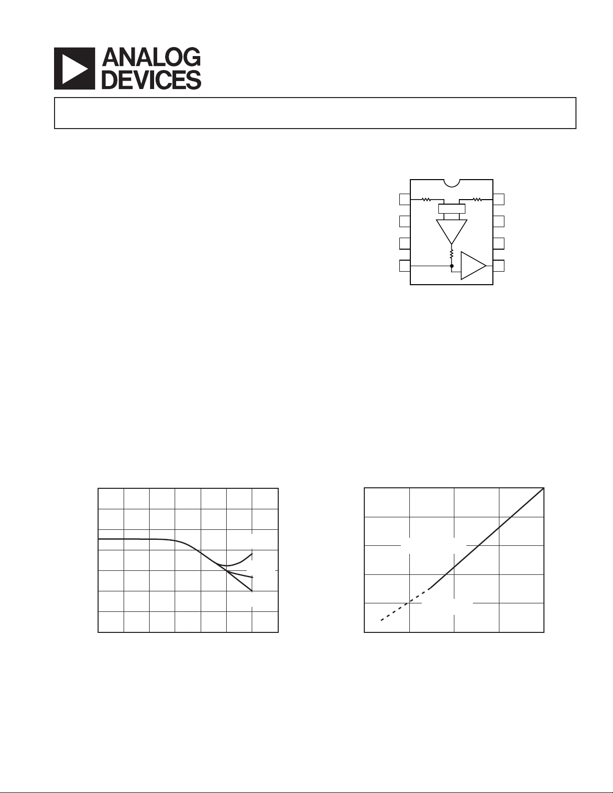
CONNECTION DIAGRAM
8-Lead Plastic Mini-DIP (N)
and SOIC (R) Packages
200k⍀
1
–IN
ANALOG
GND
–V
FILTER
2
3
S
100k⍀
4
AD626
range of this amplifi er is equal to 6 (+V
1/6
G = 30
G
200k⍀
=
2
S
+IN
8
7
G = 100
+V
6
S
5
OUT
– 1 V) which pro vides a
+24 V CMR while operating from a +5 V sup ply. Fur ther more,
the AD626 features a CMR of 90 dB typ.
The amplifi er’s inputs are protected against continuous overload of
up to 50 V, and RFI fi lters are included in the attenuator network.
The output range is +0.03 V to +4.9 V using a +5 V sup ply. The
amplifi er provides a preset gain of 10, but gains be tween 10 and
100 can be easily con fi g ured with an external re sis tor. Fur ther more, a gain of 100 is available by connecting the G = 100 pin to
analog ground. The AD626 also offers low-pass fi lter capability by
connecting a ca pac i tor between the fi lter pin and analog ground.
The AD626A and AD626B operate over the industrial tem per a ture
range of –40°C to +85°C. The AD626 is available in two 8-lead
packages: a plastic mini-DIP and SOIC.
140
120
100
80
60
40
COMMON-MODE REJECTION – dB
20
0
1
0.1
FREQUENCY – Hz
G = 10, 100
V
= +5V
S
G = 100
V
= ⴞ5V
S
G = 10
V
= ⴞ5V
S
100k10k 1k100 10
1M
Figure 1. Common-Mode Rejection vs. Frequency
REV. D
Information furnished by Analog Devices is be lieved to be accurate and
reliable. However, no responsibility is assumed by Analog Devices for its
use, nor for any infringements of patents or other rights of third parties
that may result from its use. No license is granted by implication or otherwise under any patent or patent rights of Analog Devices. Trademarks and
registered trademarks are the property of their respective companies.
25
20
15
10
5
INPUT COMMON-MODE RANGE – V
0
1
ⴞVCM FOR SINGLE
AND DUAL SUPPLIES
ⴞVCM FOR DUAL
SUPPLIES ONLY
2
SUPPLY VOLTAGE – ⴞV
3
4
5
Figure 2. Input Common-Mode Range vs. Supply
One Technology Way, P.O. Box 9106, Norwood, MA 02062-9106, U.S.A.
Tel: 781/329-4700 www.analog.com
Fax: 781/326-8703 © 2003 Analog Devices, Inc. All rights reserved.
Page 2

AD626–SPECIFICATIONS
冑
冑
SINGLE SUPPLY
(@+VS = +5 V and TA = 25ⴗC, un less oth er wise noted.)
Model AD626A AD626B
Parameter Condition Min Typ Max Min Typ Max Unit
GAIN
Gain Accuracy Total Error
Gain = 10 @ V
Gain = 100 @ V
= T
Over Temperature, T
MIN
to T
A
G = 10 50 30 ppm/°C
MAX
≥ 100 mV dc 0.4 1.0 0.2 0.6 %
OUT
≥ 100 mV dc 0.1 1.0 0.5 0.6 %
OUT
G = 100 150 120 ppm/°C
Gain Linearity
Gain = 10 @ V
Gain = 100 @ V
≥ 100 mV dc 0.014 0.016 0.014 0.016 %
OUT
≥ 100 mV dc 0.014 0.02 0.014 0.02 %
OUT
OFFSET VOLTAGE
Input Offset Voltage 1.9 2.5 1.9 2.5 mV
vs. Temperature T
vs. Temperature T
MIN
MIN
to T
to T
, G = 10 or 100 2.9 2.9 mV
MAX
, G = 10 or 100 6 6 µV/°C
MAX
vs. Supply Voltage (PSR)
+PSR 74 80 74 80 dB
–PSR 64 66 64 66 dB
COMMON-MODE REJECTION R
+CMR Gain = 10, 100 f = 100 Hz, V
±CMR Gain = 10, 100 f = 10 kHz, V
–CMR Gain = 10, 100* f = 100 Hz, V
= 10 k⍀
L
= +24 V 66 90 80 90 dB
CM
= +6 V 55 64 55 64 dB
CM
= –2 V 60 85 73 85 dB
CM
COMMON-MODE VOLTAGE RANGE
+CMV Gain = 10 CMR > 85 dB +24 +24 V
–CMV Gain = 10 CMR > 85 dB –2 –2 V
INPUT
Input Resistance
Differential 200 200 k⍀
Common-Mode 100 100 k⍀
Input Voltage Range (Common-Mode) 6 (V
– l) 6 (VS – l) V
S
OUTPUT
Output Voltage Swing R
= 10 k⍀
L
Positive Gain = 10 4.7 4.90 4.7 4.90 V
Gain = 100 4.7 4.90 4.7 4.90 V
Negative Gain = 10 0.03 0.03 V
Gain = 100 0.03 0.03 V
Short Circuit Current
+I
12 12 mA
SC
NOISE
Voltage Noise RTI
Gain = 10 f = 0.1 Hz–10 Hz 2 2 µV p-p
Gain = 100 f = 0.1 Hz–10 Hz 2 2 µV p-p
Gain = 10 f = 1 kHz 0.25 0.25 µV/
Gain = 100 f = 1 kHz 0.25 0.25 µV/
Hz
Hz
DYNAMIC RESPONSE
–3 dB Bandwidth V
Slew Rate, T
MIN
to T
Gain = 10 0.17 0.22 0.17 0.22 V/µs
MAX
= +1 V dc 100 100 kHz
OUT
Gain = 100 0.1 0.17 0.1 0.17 V/µs
Settling Time to 0.01%, 1 V Step 24 22 µs
POWER SUPPLY
Operating Range T
MIN
to T
A
2.4 5 12 2.4 5 10 V
MAX
= T
Quiescent Current Gain = 10 0.16 0.20 0.16 0.20 mA
Gain = 100 0.23 0.29 0.23 0.29 mA
TRANSISTOR COUNT Number of Transistors 46 46
*At temperatures above 25°C, –CMV degrades at the rate of 12 mV/°C; i.e., @ 25°C CMV = –2 V, @ 85°C CMV = –1.28 V.
Specifi cations subject to change without notice.
–2–
REV. D
Page 3

AD626
冑
冑
DUAL SUPPLY
(@+VS = ⴞ5 V and TA = 25ⴗC, un less oth er wise noted.)
Model AD626A AD626B
Parameter Condition Min Typ Max Min Typ Max Unit
GAIN
Gain Accuracy Total Error
Gain = 10 R
= 10 k⍀ 0.2 0.5 0.1 0.3 %
L
Gain = 100 0.25 1.0 0.15 0.6 %
Over Temperature, T
MIN
to T
A
G = 10 50 30 ppm/°C
MAX
= T
G = 100 100 80 ppm/°C
Gain Linearity
Gain = 10 0.045 0.055 0.045 0.055 %
Gain = 100 0.01 0.015 0.01 0.015 %
OFFSET VOLTAGE
Input Offset Voltage 50 500 50 250 µV
vs. Temperature T
vs. Temperature T
MIN
MIN
to T
to T
, G = 10 or 100 1.0 0.5 mV
MAX
, G = 10 or 100 1.0 0.5 µV/°C
MAX
vs. Supply Voltage (PSR)
+PSR 74 80 74 80 dB
–PSR 64 66 64 66 dB
COMMON-MODE REJECTION R
+CMR Gain = 10, 100 f = 100 Hz, V
±CMR Gain = 10, 100 f = 10 kHz, V
= 10 k⍀
L
= +24 V 66 90 80 90 dB
CM
= 6 V 55 60 55 60 dB
CM
COMMON-MODE VOLTAGE RANGE
+CMV Gain = 10 CMR > 85 dB 26.5 26.5 V
–CMV Gain = 10 CMR > 85 dB 32.5 32.5 V
INPUT
Input Resistance
Differential 200 200 k⍀
Common-Mode 110 110 k⍀
Input Voltage Range (Common-Mode) 6 (V
– l) 6 (VS – l) V
S
OUTPUT
Output Voltage Swing R
= 10 k⍀
L
Positive Gain = 10, 100 4.7 4.90 4.7 4.90 V
Negative Gain = 10 –1.65 –2.1 –1.65 –2.1 V
Gain = 100 –1.45 –1.8 –1.45 –1.8 V
Short Circuit Current
+I
–I
12 12 mA
SC
0.5 0.5 mA
SC
NOISE
Voltage Noise RTI
Gain = 10 f = 0.1 Hz–10 Hz 2 2 µV p-p
Gain = 100 f = 0.1 Hz–10 Hz 2 2 µV p-p
Gain = 10 f = 1 kHz 0.25 0.25 µV/
Gain = 100 f = 1 kHz 0.25 0.25 µV/
Hz
Hz
DYNAMIC RESPONSE
–3 dB Bandwidth V
Slew Rate, T
MIN
to T
Gain = 10 0.17 0.22 0.17 0.22 V/µs
MAX
= +1 V dc 100 100 kHz
OUT
Gain = 100 0.1 0.17 0.1 0.17 V/µs
Settling Time to 0.01%, 1 V Step 24 22 µs
POWER SUPPLY
Operating Range T
MIN
to T
A
⫾1.2 ⫾5 ⫾6 ⫾1.2 ⫾5 ⫾6 V
MAX
= T
Quiescent Current Gain = 10 1.5 2 1.5 2 mA
Gain = 100 1.5 2 1.5 2 mA
TRANSISTOR COUNT Number of Transistors 46 46
Specifi cations subject to change without notice.
REV. D
–3–
Page 4
AD626
ABSOLUTE MAXIMUM RATINGS
Supply Voltage . . . . . . . . . . . . . . . . . . . . . . . . . . . . . . . . . +36 V
Internal Power Dissipation
2
1
Peak Input Voltage . . . . . . . . . . . . . . . . . . . . . . . . . . . . . . +60 V
Maximum Reversed Supply Voltage Limit . . . . . . . . . . . . . –34 V
Output Short Circuit Duration . . . . . . . . . . . . . . . . . . Indefi nite
Storage Temperature Range (N, R) . . . . . . . . . –65°C to +125°C
Operating Temperature Range
AD626A/AD626B . . . . . . . . . . . . . . . . . . . . –40°C to +85°C
Lead Temperature Range (Soldering 60 sec) . . . . . . . . . +300°C
ORDERING GUIDE
Temperature Package Package
Model Range Description Option
AD626AN –40°C to +85°C Plastic DIP N-8
AD626AR –40°C to +85°C Small Outline IC R-8
AD626BN –40°C to +85°C Plastic DIP N-8
AD626AR-REEL –40°C to +85°C 13" Tape and Reel
AD626AR-REEL7 –40°C to +85°C 7" Tape and Reel
NOTES
1
Stresses above those listed under Absolute Max i mum Ratings may cause per ma nent
damage to the device. This is a stress rating only; functional operation of the device
at these or any other conditions above those indicated in the operational section of
this specifi cation is not implied. Exposure to ab so lute maximum rating con di tions
for extended periods may affect device re li abil i ty.
2
8-Lead Plastic Package: JA = 100°C/W; JC = 50°C/W.
8-Lead SOIC Package: JA = 155°C/W;
= 40°C/W.
JC
METALLIZATION PHOTOGRAPH
Dimensions shown in inches and (mm).
CAUTION
ESD (electrostatic discharge) sensitive device. Electrostatic charges as high as 4000 V readily ac cu mu late
on the human body and test equipment and can discharge without detection. Although the AD626 features
proprietary ESD pro tec tion circuitry, permanent damage may occur on devices subjected to high energy
electrostatic discharges. Therefore, proper ESD pre cau tions are rec om mend ed to avoid per for mance
deg ra da tion or loss of functionality.
–4–
REV. D
Page 5

Typical Performance Characteristics–AD626
25
20
15
10
5
INPUT COMMON-MODE RANGE – V
0
1
ⴞVCM FOR SINGLE
AND DUAL SUPPLIES
ⴞVCM FOR DUAL
SUPPLIES ONLY
2
SUPPLY VOLTAGE – ⴞV
3
4
TPC 1. Input Common-Mode Range vs. Supply
5
TA = 25ⴗC
4
SINGLE AND
DUAL SUPPLY
3
6
VS = ⴞ5V
5
GAIN = 10, 100
4
3
2
1
POSITIVE OUTPUT VOLTAGE – V
0
5
–1
10 100 10k 1k
LOAD RESISTANCE – ⍀
TPC 4. Positive Output Voltage Swing vs. Resistive Load
–6
–5
–4
–3
GAIN = 10
2
DUAL SUPPLY
1
POSITIVE OUTPUT VOLTAGE SWING – V
0
0
1
ONLY
SUPPLY VOLTAGE – V
4 3 2
5
TPC 2. Positive Output Voltage Swing vs. Supply Voltage
–5
TA = 25ⴗC
–4
–3
–2
–1
NEGATIVE OUTPUT VOLTAGE SWING – V
0
0
1
DUAL SUPPLY
ONLY
SUPPLY VOLTAGE – V
4 3 2
5
–2
–1
NEGATIVE OUTPUT VOLTAGE – V
0
1
100 1k 100k 10k
LOAD RESISTANCE – ⍀
GAIN = 100
TPC 5. Negative Output Voltage Swing vs. Resistive Load
30
V
20
10
CHANGE IN OFFSET VOLTAGE –
0
0
1432
WARM-UP TIME – Minutes
5
TPC 3. Negative Output Voltage Swing vs. Supply Voltage
REV. D
TPC 6. Change in Input Offset Voltage vs. Warm-Up Time
–5–
Page 6

AD626
1000
100
10
CLOSED-LOOP GAIN
0
10 100 1M100k10k1k
GAIN = 100
GAIN = 10
VS = +5V
SINGLE SUPPLY
VS = ⴞ5V
DUAL SUPPLY
FREQUENCY – Hz
TPC 7. Closed-Loop Gain vs. Frequency
140
120
100
80
60
VS = ⴞ5V
DUAL SUPPLY
G = 10, 100
V
= +5
S
G = 100
V
= ⴞ5
S
100
95
90
85
80
75
COMMON-MODE REJECTION – dB
70
65
20
VS = ⴞ5
22
INPUT COMMON-MODE VOLTAGE – V
28 26 24
30
TPC 10. Common-Mode Rejection vs. Input
Common- Mode Voltage for Dual-Supply Operation
100
G = 10, 100
90
80
40
COMMON-MODE REJECTION – dB
20
0
0.1
1
FREQUENCY – Hz
G = 10
V
= ⴞ5
S
100k10k 1k100 10
TPC 8. Common-Mode Rejection vs. Frequency
100
95
90
85
80
75
COMMON-MODE REJECTION – dB
70
65
–5
G = 10, 100
= +5
V
S
0
INPUT COMMON-MODE VOLTAGE – V
20 15 10 5
25
1M
70
COMMON-MODE REJECTION – dB
60
080
20
INPUT SOURCE RESISTANCE MISMATCH – ⍀
40
60
TPC 11. Common-Mode Rejection vs. Input Source
Resistance Mismatch
0.7
CURVE APPLIES TO
ALL SUPPLY VOLTAGES
0.6
AND GAINS BETWEEN 10 AND 100
0.5
TOTAL GAIN ERROR =
GAIN ACCURACY (FROM SPEC TABLE)
0.4
+ ADDITIONAL GAIN ERROR
0.3
0.2
ADDITIONAL GAIN ERROR – %
0.1
0.0
10 100 1k
SOURCE RESISTANCE MISMATCH – ⍀
TPC 9. Common-Mode Rejection vs. Input CommonMode Voltage for Single-Supply Operation
–6–
TPC 12. Additional Gain Error vs. Source
Resistance Mismatch
REV. D
Page 7

0.16
0.15
0.14
AD626
G = 10
0.13
QUIESCENT CURRENT – mA
0.12
1 5
2
SUPPLY VOLTAGE – V
3
4
TPC 13. Quiescent Supply Current vs. Supply Voltage
for Single-Supply Operation
2.0
1.5
1.0
0.5
QUIESCENT CURRENT – mA
0
ⴞ1 ⴞ5
ⴞ2
SUPPLY VOLTAGE – V
ⴞ3
ⴞ4
V PER VERTICAL DIVISION
2
5 SECONDS PER HORIZONTAL DIVISION
TPC 16. 0.1 Hz to 10 Hz RTI Voltage Noise. VS = ±5 V,
Gain = 100
100
80
FOR VS = ⴞ5V AND +5V
60
40
CLOSED-LOOP GAIN
20
0
110 1M100k10k1k100
VALUE OF RESISTOR R
– ⍀
TPC 14. Quiescent Supply Current vs. Supply Voltage
for Dual-Supply Operation
10
1.0
GAIN = 10, 100
0.1
VOLTAGE NSD – V/ Hz
0.01
110 100k10k1k100
VS = ⴞ5V DUAL SUPPLY
FREQUENCY – Hz
TPC 15. Noise Voltage Spectral Density vs. Frequency
TPC 17. Closed-Loop Gain vs. R
140
120
100
80
60
40
POWER SUPPLY REJECTION – dB
20
1 0.1
SINGLE
+PSRR
FREQUENCY – Hz
ALL CURVES FOR
GAINS OF 10 OR 100
SINGLE AND DUAL
–PSRR
G
DUAL
DUAL
+PSRR
+PSRR
100k10k 1k100 10
TPC 18. Power Supply Rejection vs. Frequency
1M
REV. D
–7–
Page 8

AD626
100
90
10
0%
TPC 19. Large Signal Pulse Response. VS = ±5 V, G = 10
100
90
10
0%
100
90
10
0%
TPC 22. Large Signal Pulse Response. VS = +5 V, G = 100
100
90
10
0%
TPC 20. Large Signal Pulse Response. VS = ±5 V, G = 100
100
90
10
0%
TPC 21. Large Signal Pulse Response. VS = +5 V, G = 10
TPC 23. Settling Time. VS = ±5 V, G = 10
500mV
100
90
10
0%
TPC 24. Settling Time. VS = ±5 V, G = 100
–8–
REV. D
Page 9

AD626
100
90
10
0%
TPC 25. Settling Time. VS = +5 V, G = 10
ERROR
OUT
INPUT
20V p–p
10k⍀
10k⍀
1k⍀
2k⍀
AD626
10k⍀
+V
S
–V
S
Figure 3. Settling Time Test Circuit
THEORY OF OPERATION
The AD626 is a differential amplifi er con sist ing of a precision
bal anced attenuator, a very low drift preamplifi er (A1), and an
out put buffer amplifi er (A2). It has been designed so that small
differential signals can be accurately am pli fi ed and fi ltered in the
presence of large common -mode voltages (V
), without the use
CM
of any other active components.
100
90
10
0%
TPC 26. Settling Time. VS = +5 V, G = 100
Figure 4 shows the main elements of the AD626. The signal in puts
at Pins 1 and 8 are fi rst applied to dual resistive at ten u a tors R1
through R4 whose purpose is to reduce the peak com mon-mode
voltage at the input to the preamplifi er—a feed back stage based
on the very low drift op amp A1. This allows the dif feren tial
input voltage to be accurately amplifi ed in the pres ence of large
common-mode volt ag es six times greater than that which can be
tol er at ed by the actual input to A1. As a re sult, the in put CMR
ex tends to six times the quantity (V
– 1 V). The over all common -
S
mode error is min i mized by precise laser-trimming of R3 and R4,
thus giving the AD626 a common-mode re jec tion ra tio (CMRR)
of at least 10,000:1 (80 dB).
To minimize the effect of spurious RF signals at the inputs due to
rectifi cation at the input to A1, small fi lter capacitors C1 and C2
are included.
The output of A1 is connected to the in put of A2 via a 100 k⍀
(R12) resistor to facilitate the low-pass fi ltering of the sig nal of
in ter est (see Low-Pass Filtering section).
The 200 k⍀ input impedance of the AD626 requires that the source
re sis tance driving this amplifi er be low in val ue (<1 k⍀)—this is
REV. D
+IN
–IN
C1
R1
200k⍀
R2
200k⍀
R11
10k⍀R6500⍀
5pF
41k⍀
R3
GND
+V
S
A1
C2
5pF
R4
R5
4.2k⍀
41k⍀
R7
500⍀
R9
10k⍀
10k⍀
R8
Figure 4. Simplifi ed Schematic
–9–
R12
100k⍀
R10
10k⍀
FILTER
R17
95k⍀
R14
555⍀
GAIN = 100
AD626
A2
R15
10k⍀
R13
10k⍀
OUT
–V
S
Page 10

AD626
necessary to min i mize gain error. Also, any mis match be tween the
total source re sis tance at each input will af fect gain ac cu ra cy and
common -mode rejection (CMR). For ex am ple: when operating at
a gain of 10, an 80 ⍀ mismatch in the source re sis tance between
the inputs will degrade CMR to 68 dB.
The output buffer, A2, operates at a gain of 2 or 20, thus setting
the overall, precalibrated gain of the AD626 (with no ex ter nal
com po nents) at 10 or 100. The gain is set by the feedback net work
around amplifi er A2.
The output of amplifi er A2 relies on a 10 k⍀ resistor to –V
“pull-down.” For single-supply operation, (–V
= “GND”), A2
S
for
S
can drive a 10 k⍀ ground ref er enced load to at least +4.7 V. The
min i mum, nominally “zero,” output voltage will be 30 mV. For
dual-supply op er a tion (±5 V), the positive output voltage swing
will be the same as for a single supply. The negative swing will be
to –2.5 V, at G = 100, limited by the ratio:
RR
+
–V
S
15 14
×
RRR
++
13 14 15
The negative range can be extended to –3.3 V (G = 100) and –4 V
(G = 10) by add ing an external 10 k⍀ pull-down from the out put
. This will add 0.5 mA to the AD626’s qui es cent cur rent,
to –V
S
bringing the total to 2 mA.
The AD626’s 100 kHz bandwidth at G = 10 and 100 (a 10 MHz
gain bandwidth) is much higher than can be obtained with low
power op amps in discrete dif fer en tial amplifi er circuits. Fur ther more, the AD626 is stable driving capacitive loads up to 50 pF
(G10) or 200 pF (G100). Capacitive load drive can be increased
to 200 pF (G10) by connecting a 100 ⍀ resistor in series with the
AD626’s output and the load.
ADJUSTING THE GAIN OF THE AD626
The AD626 is easily confi gured for gains of 10 or 100. Figure 5
shows that for a gain of 10, Pin 7 is simply left un con nect ed; similarly, for a gain of 100, Pin 7 is grounded, as shown in Fig ure 6.
Gains between 10 and 100 are easily set by connecting a vari able
resistance between Pin 7 and Analog GND, as shown in Fig ure 7.
Because the on-chip resistors have an absolute tol er ance of ±20%
(although they are ratio matched to within 0.1%), at least a 20%
adjustment range must be provided. The values shown in the
table in Figure 7 provide a good trade-off be tween gain set range
and resolution, for gains from 11 to 90.
+INPUT
+INPUT
200k⍀ 200k⍀
–INPUT
–V
S
0.1F
1
2
3
4
–IN
ANALOG
GND
–V
S
FILTER
1/6
G = 30
100k⍀
G = 2
+IN
G = 100
+V
OUT
8
7
0.1F
+V
S
OUTPUT
6
S
5
AD626
Figure 6. AD626 Confi gured for a Gain of 100
+INPUT
200k⍀ 200k⍀
–INPUT
–V
S
0.1F
FILTER
(OPTIONAL)
–IN
1
ANALOG
2
GND
–V
3
S
FILTER
4
CF
1/6
G = 30
100k⍀
AD626
CORNER FREQUENCY OF FILTER =
RESISTOR VALUES FOR GAIN ADJUSTMENT
GAIN RANGE RG(⍀) RH(⍀)
11 – 20
20 – 40
40 – 80
80 – 100
100k
10k
1k
100
G = 2
+IN
G = 100
+V
OUT
2CF (100k⍀)
4.99k
802
80
2
8
RH
7
6
S
5
RG
+V
S
0.1F
OUTPUT
1
Figure 7. Recommended Circuit for Gain Adjustment
SINGLE-POLE LOW-PASS FILTERING
A low-pass fi lter can be easily implemented by using the fea tures
provided by the AD626.
By simply connecting a capacitor between Pin 4 and ground,
a single-pole low-pass fi lter is created, as shown in Figure 8.
+INPUT
–INPUT
–V
S
0.1F
1
2
3
4
–IN
ANALOG
GND
–V
S
FILTER
1/6
G = 30
100k⍀
G = 2
+IN
G = 10
+V
OUT
S
200k⍀ 200k⍀
AD626
Figure 5. AD626 Confi gured for a Gain of 10
8
NOT
7
CONNECTED
6
5
+V
0.1F
S
OUTPUT
–10–
–INPUT
–IN
1
ANALOG
2
GND
–V
3
S
FILTER
4
CF
CORNER FREQUENCY OF FILTER =
AD626
1/6
G = 30
100k⍀
G = 2
+IN
G = 100
+V
S
OUT
2CF (100k⍀)
8
7
6
5
1
200k⍀ 200k⍀
Figure 8. A One-Pole Low-Pass Filter Circuit
Which Operates from a Single +10 V Supply
+10V
0.1F
OUTPUT
REV. D
Page 11

AD626
CURRENT SENSOR INTERFACE
A typical current sensing application, making use of the large
common-mode range of the AD626, is shown in Figure 9. The
cur rent being measured is sensed across resistor R
should be less than 1 k⍀ and should be selected so that the
R
S
. The value of
S
average differential voltage across this resistor is typically 100 mV.
To produce a full-scale output of +4 V, a gain of 40 is used adjustable by ±20% to absorb the tolerance in the sense re sis tor. Note
that there is suffi cient headroom to allow at least a 10% over range
(to +4.4 V).
CURRENT IN
URRENT OUT
OPTIONAL
LOW-PASS
CURRENT
SENSOR
FILTER
–V
0.1F
R
S
S
CF
200k⍀ 200k⍀
–IN
1
ANALOG
2
GND
–V
3
S
FILTER
4
100k⍀
1/6
G = 30
G = 2
+IN
G = 100
+V
OUT
8
RH
7
6
S
5
0.1F
RG
+V
S
OUTPUT
AD626
Figure 9. Current Sensor Interface
BRIDGE APPLICATION
Figure 10 shows the AD626 in a typical bridge application. Here,
the AD626 is set to operate at a gain of 100, using dual-sup ply
voltages and offering the option of low-pass fi ltering.
+V
S
200k⍀ 200k⍀
–5V
0.1F
CF
OPTIONAL
LOW-PASS
FILTER
1
2
3
4
–IN
ANALOG
GND
–V
S
FILTER
AD626
1/6
G = 30
100k⍀
G = 2
+IN
G = 100
+V
OUT
8
7
6
S
5
+5V
0.1F
OUTPUT
Figure 10. A Typical Bridge Application
REV. D
–11–
Page 12

AD626
OUTLINE DIMENSIONS
8-Lead Standard Small Outline Package [SOIC]
Narrow Body
(R-8)
Dimensions shown in millimeters and (inches)
5.00 (0.1968)
4.80 (0.1890)
4.00 (0.1574)
3.80 (0.1497)
0.25 (0.0098)
0.10 (0.0040)
COPLANARITY
0.10
COMPLIANT TO JEDEC STANDARDS MS-012AA
CONTROLLING DIMENSIONS ARE IN MILLIMETERS; INCH DIMENSIONS
(IN PARENTHESES) ARE ROUNDED-OFF MILLIMETER EQUIVALENTS FOR
REFERENCE ONLY AND ARE NOT APPROPRIATE FOR USE IN DESIGN
85
1.27 (0.0500)
SEATING
PLANE
BSC
6.20 (0.2440)
5.80 (0.2284)
41
1.75 (0.0688)
1.35 (0.0532)
0.51 (0.0201)
0.33 (0.0130)
0.25 (0.0098)
0.19 (0.0075)
0.50 (0.0196)
0.25 (0.0099)
8ⴗ
0ⴗ
1.27 (0.0500)
0.41 (0.0160)
8-Lead Plastic Dual-In Line Package [PDIP]
(N-8)
Dimensions shown in inches and (millimeters)
0.375 (9.53)
0.365 (9.27)
0.355 (9.02)
8
1
0.100 (2.54)
0.180
(4.57)
MAX
0.150 (3.81)
0.130 (3.30)
0.110 (2.79)
0.022 (0.56)
0.018 (0.46)
0.014 (0.36)
CONTROLLING DIMENSIONS ARE IN INCHES; MILLIMETER DIMENSIONS
(IN PARENTHESES) ARE ROUNDED-OFF INCH EQUIVALENTS FOR
REFERENCE ONLY AND ARE NOT APPROPRIATE FOR USE IN DESIGN
COMPLIANT TO JEDEC STANDARDS MO-095AA
BSC
5
4
0.295 (7.49)
0.285 (7.24)
0.275 (6.98)
0.015
(0.38)
MIN
SEATING
PLANE
0.060 (1.52)
0.050 (1.27)
0.045 (1.14)
0.325 (8.26)
0.310 (7.87)
0.300 (7.62)
0.150 (3.81)
0.135 (3.43)
0.120 (3.05)
0.015 (0.38)
0.010 (0.25)
0.008 (0.20)
C00781–0–1/03(D)PRINTED IN U.S.A.
ⴛ45ⴗ
Revision History
Location Page
1/03—Data Sheet changed from REV. C to REV. D.
Renumbered Figures and TPCs . . . . . . . . . . . . . . . . . . . . . . . . . . . . . . . . . . . . . . . . . . . . . . . . . . . . . . . . . . . . . . . . . . . . . . . Universal
Edits to Figure 1 . . . . . . . . . . . . . . . . . . . . . . . . . . . . . . . . . . . . . . . . . . . . . . . . . . . . . . . . . . . . . . . . . . . . . . . . . . . . . . . . . . . . . . . . . 1
Edits to SPECIFICATIONS, Output . . . . . . . . . . . . . . . . . . . . . . . . . . . . . . . . . . . . . . . . . . . . . . . . . . . . . . . . . . . . . . . . . . . . . . . . . 3
Edit to ORDERING GUIDE . . . . . . . . . . . . . . . . . . . . . . . . . . . . . . . . . . . . . . . . . . . . . . . . . . . . . . . . . . . . . . . . . . . . . . . . . . . . . . . 4
Update to standard CAUTION/ESD Warning note and diagram . . . . . . . . . . . . . . . . . . . . . . . . . . . . . . . . . . . . . . . . . . . . . . . . . . . . 4
Edits to TPC 8 . . . . . . . . . . . . . . . . . . . . . . . . . . . . . . . . . . . . . . . . . . . . . . . . . . . . . . . . . . . . . . . . . . . . . . . . . . . . . . . . . . . . . . . . . . 6
Updated OUTLINE DIMENSIONS . . . . . . . . . . . . . . . . . . . . . . . . . . . . . . . . . . . . . . . . . . . . . . . . . . . . . . . . . . . . . . . . . . . . . . . . 12
–12–
REV. D
 Loading...