

Page 1
Low Cost
a
FEATURES
Easy to Use
Low Cost Solution
Higher Performance than Two or Three Op Amp Design
Unity Gain with No External Resistor
Optional Gains with One External Resistor
(Gain Range 2 to 1000)
Wide Power Supply Range (ⴞ2.6 V to ⴞ15 V)
Available in 8-Lead PDIP and SOIC
Low Power, 1.5 mA max Supply Current
GOOD DC PERFORMANCE
0.15% Gain Accuracy (G = 1)
125 V max Input Offset Voltage
1.0 V/ⴗC max Input Offset Drift
5 nA max Input Bias Current
66 dB min Common-Mode Rejection Ratio (G = 1)
NOISE
12 nV/√Hz @ 1 kHz Input Voltage Noise
0.60 V
EXCELLENT AC CHARACTERISTICS
800 kHz Bandwidth (G = 10)
10 s Settling Time to 0.1% @ G = 1–100
1.2 V/s Slew Rate
APPLICATIONS
Transducer Interface
Low Cost Thermocouple Amplifier
Industrial Process Controls
Difference Amplifier
Low Cost Data Acquisition
p-p Noise (0.1 Hz to 10 Hz, G = 10)
Instrumentation Amplifier
AD622
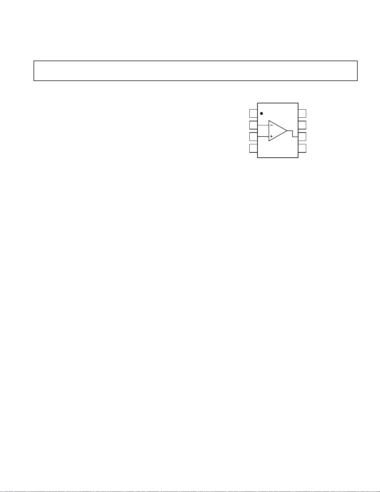
CONNECTION DIAGRAM
1
R
G
–IN
2
3
+IN
–V
4
S
PRODUCT DESCRIPTION
AD622
The AD622 is a low cost, moderately accurate instrumentation
amplifier that requires only one external resistor to set any gain
between 2 and 1,000. Or for a gain of 1, no external resistor
is required. The AD622 is a complete difference or subtracter
amplifier “system” while providing superior linearity and commonmode rejection by incorporating precision laser trimmed resistors.
The AD622 replaces low cost, discrete, two or three op amp
instrumentation amplifier designs and offers good commonmode rejection, superior linearity, temperature stability, reliability, and board area consumption. The low cost of the AD622
eliminates the need to design discrete instrumentation amplifiers to meet stringent cost targets. While providing a lower cost
solution, it also provides performance and space improvements.
8
7
6
5
R
G
+V
S
OUTPUT
REF
REV. C
Information furnished by Analog Devices is believed to be accurate and
reliable. However, no responsibility is assumed by Analog Devices for its
use, nor for any infringements of patents or other rights of third parties
which may result from its use. No license is granted by implication or
otherwise under any patent or patent rights of Analog Devices.
One Technology Way, P.O. Box 9106, Norwood, MA 02062-9106, U.S.A.
Tel: 781/329-4700 World Wide Web Site: http://www.analog.com
Fax: 781/326-8703 © Analog Devices, Inc., 1999
Page 2

AD622–SPECIFICATIONS
(typical @ +25ⴗC, VS = ⴞ15 V, and RL = 2 k⍀ unless otherwise noted)
AD622
Model Conditions Min Typ Max Units
GAIN G = 1 + (50.5 k/R
Gain Range 1 1000
Gain Error
1
V
OUT
= ±10 V
)
G
G = 1 0.05 0.15 %
G = 10 0.2 0.50 %
G = 100 0.2 0.50 %
G = 1000 0.2 0.50 %
Nonlinearity, V
G = 1–1000 R
G = 1–100 R
Gain vs. Temperature Gain = 1 10 ppm/°C
VOLTAGE OFFSET (Total RTI Error = V
Input Offset, V
OSI
Average TC V
Output Offset, V
OSO
Average TC V
= ±10 V
OUT
= 10 kΩ 10 ppm
L
= 2 kΩ 10 ppm
L
Gain >1
V
V
1
+ V
OSO
/G)
= ±5 V to ±15 V 60 125 µV
S
= ±5 V to ±15 V 1.0 µV/°C
S
= ±5 V to ±15 V 600 1500 µV
S
= ±5 V to ±15 V 15 µV/°C
S
OSI
–50 ppm/°C
Offset Referred to the
Input vs.
Supply (PSR) V
= ±5 V to ±15 V
S
G = 1 80 100 dB
G = 10 95 120 dB
G = 100 110 140 dB
G = 1000 110 140 dB
INPUT CURRENT
Input Bias Current 2.0 5.0 nA
Average TC 3.0 pA/°C
Input Offset Current 0.7 2.5 nA
Average TC 2.0 pA/°C
INPUT
Input Impedance
Differential 10储2GΩ储pF
Common-Mode 10储2GΩ储pF
Input Voltage Range
Over Temperature –V
Over Temperature –V
2
V
= ±2.6 V to ±5 V –V
S
= ±5 V to ±18 V –V
V
S
+ 1.9 +VS – 1.2 V
S
+ 2.1 +VS – 1.3 V
S
+ 1.9 +VS – 1.4 V
S
+ 2.1 +VS – 1.4 V
S
Common-Mode Rejection
Ratio DC to 60 Hz with
1 kΩ Source Imbalance V
= 0 V to ±10 V
CM
G = 1 66 78 dB
G = 10 86 98 dB
G = 100 103 118 dB
G = 1000 103 118 dB
OUTPUT
Output Swing R
Over Temperature –V
Over Temperature –V
= 10 kΩ,
L
= ±2.6 V to ±5 V –V
V
S
V
= ±5 V to ±18 V –V
S
+ 1.1 +VS – 1.2 V
S
+ 1.4 +VS – 1.3 V
S
+ 1.2 +VS – 1.4 V
S
+ 1.6 +VS – 1.5 V
S
Short Current Circuit ±18 mA
–2–
REV. C
Page 3
AD622
AD622
Model Conditions Min Typ Max Units
DYNAMIC RESPONSE
Small Signal –3 dB Bandwidth
G = 1 1000 kHz
G = 10 800 kHz
G = 100 120 kHz
G = 1000 12 kHz
Slew Rate 1.2 V/µs
Settling Time to 0.1% 10 V Step
G = 1–100 10 µs
NOISE
Voltage Noise, 1 kHz
Input, Voltage Noise, e
Output, Voltage Noise, e
ni
no
Total RTI Noise = (e
RTI, 0.1 Hz to 10 Hz
G = 1 4.0 µV p-p
G = 10 0.6 µV p-p
G = 100–1000 0.3 µV p-p
Current Noise f = 1 kHz 100 fA/√Hz
0.1 Hz to 10 Hz 10 pA p-p
REFERENCE INPUT
R
IN
I
IN
V
, V
IN+
= 0 +50 +60 µA
REF
Voltage Range –V
Gain to Output 1 ± 0.0015
POWER SUPPLY
Operating Range
Quiescent Current V
3
= ±2.6 V to ±18 V 0.9 1.3 mA
S
Over Temperature 1.1 1.5 mA
TEMPERATURE RANGE
For Specified Performance –40 to +85 °C
NOTES
1
Does not include effects of external resistor RG.
2
One input grounded. G = 1.
3
This is defined as the same supply range that is used to specify PSR.
Specifications subject to change without notice.
2
) +(e
ni
2
/ G)
no
12 nV/√Hz
72 nV/√Hz
20 kΩ
+ 1.6 +VS – 1.6 V
S
±2.6 ±18 V
REV. C
–3–
Page 4
AD622
ABSOLUTE MAXIMUM RATINGS
Supply Voltage . . . . . . . . . . . . . . . . . . . . . . . . . . . . . . . . ±18 V
Internal Power Dissipation
2
. . . . . . . . . . . . . . . . . . . . 650 mW
Input Voltage (Common Mode) . . . . . . . . . . . . . . . . . . . ±V
Differential Input Voltage . . . . . . . . . . . . . . . . . . . . . . . ±25 V
Output Short Circuit Duration . . . . . . . . . . . . . . . . Indefinite
Storage Temperature Range (N, R) . . . . . . . –65°C to +125°C
Operating Temperature Range
AD622A . . . . . . . . . . . . . . . . . . . . . . . . . . . – 40°C to +85°C
Lead Temperature Range
1
ORDERING GUIDE
Temperature Package
Model Range Option*
S
AD622AN –40°C to +85°C N-8
AD622AR –40°C to +85°C SO-8
AD622AR-REEL –40°C to +85°C 13" Reel
AD622AR-REEL7 –40°C to +85°C 7" Reel
*N = Plastic DIP, SO = Small Outline.
(Soldering 10 seconds) . . . . . . . . . . . . . . . . . . . . . . . +300°C
NOTES
1
Stresses above those listed under Absolute Maximum Ratings may cause perma-
nent damage to the device. This is a stress rating only; functional operation of the
device at these or any other conditions above those indicated in the operational
section of this specification is not implied. Exposure to absolute maximum rating
conditions for extended periods may affect device reliability.
2
Specification is for device in free air:
8-Lead Plastic Package: θJA = 95°C/Watt
8-Lead SOIC Package: θJA = 155°C/Watt
CAUTION
ESD (electrostatic discharge) sensitive device. Electrostatic charges as high as 4000 V readily
accumulate on the human body and test equipment and can discharge without detection.
Although the AD622 features proprietary ESD protection circuitry, permanent damage may
occur on devices subjected to high energy electrostatic discharges. Therefore, proper ESD
precautions are recommended to avoid performance degradation or loss of functionality.
WARNING!
ESD SENSITIVE DEVICE
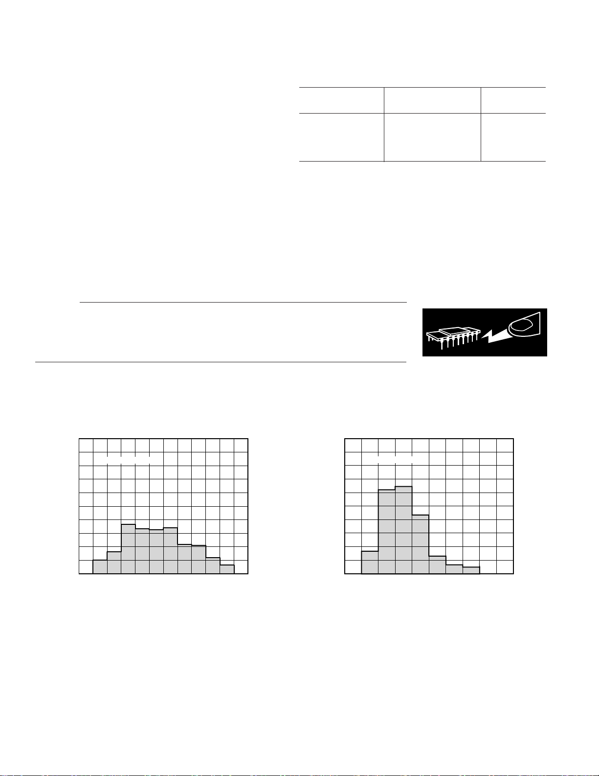
Typical Characteristics
50
SAMPLE SIZE = 191
40
30
20
PERCENTAGE OF UNITS
10
0
–0.40
OUTPUT OFFSET VOLTAGE – mV
(@ +25ⴗC, VS = ⴞ15 V, RL = 2 k⍀, unless otherwise noted)
0 0.40
0.80 1.00–1.00 –0.80
Figure 1. Typical Distribution of Output Offset Voltage
50
40
30
20
PERCENTAGE OF UNITS
10
SAMPLE SIZE = 383
0
60 80 100 120 140
COMMON-MODE REJECTION RATIO – dB
Figure 2. Typical Distribution of Common-Mode Rejection
–4–
REV. C
Page 5

AD622
FREQUENCY – Hz
0.1 1M1 10 100 1k 10k 100k
0
140
80
60
40
20
120
100
CMR – dB
G = 1000
G = 100
G = 10
G = 1
Typical Characteristics
2
1.5
1
0.5
INPUT OFFSET VOLTAGE – mV
0
051234
WARM-UP TIME – Minutes
(@ +25ⴗC, VS = ⴞ15 V, RL = 2 k⍀, unless otherwise noted)
Figure 3. Change in Input Offset Voltage vs. Warm-Up
Time
1000
GAIN = 1
100
Figure 6. CMR vs. Frequency, RTI, Zero to 1 kΩ Source
Imbalance
180
160
140
120
G = 1000
GAIN = 10
10
VOLTAGE NOISE – nV/ Hz
GAIN = 100, 1,000
GAIN = 1000
BW LIMIT
1
1 100k10 100 1k 10k
FREQUENCY – Hz
Figure 4. Voltage Noise Spectral Density vs. Frequency,
(G = 1–1000)
1000
100
CURRENT NOISE – fA/ Hz
10
0 100010
FREQUENCY – Hz
100
Figure 5. Current Noise Spectral Density vs. Frequency
100
80
POSITIVE PSR – dB
60
40
0
0.1 1M1 10 100 1k 10k 100k
FREQUENCY – Hz
G = 100
G = 10
G = 1
Figure 7a. Positive PSR vs. Frequency, RTI (G = 1–1000)
180
160
140
120
100
80
NEGATIVE PSR – dB
60
40
0
0.1 1M1 10 100 1k 10k 100k
FREQUENCY – Hz
G = 1000
G = 100
G = 10
G = 1
Figure 7b. Negative PSR vs. Frequency, RTI (G = 1–1000)
REV. C
–5–
Page 6

AD622–
Typical Characteristics
(@ +25ⴗC, VS = ⴞ15 V, RL = 2 k⍀, unless otherwise noted)
1000
100
10
GAIN – V/V
1
0
100 10M1k 10k 100k 1M
FREQUENCY – Hz
Figure 8. Gain vs. Frequency
30
VS = 615V
G = 10
20
1000
100
10
SETTLING TIME – ms
1
1 100010 100
GAIN
Figure 11. Settling Time to 0.1% vs. Gain, for a 10 V Step
10µV
100
90
ø
2V
10
OUTPUT VOLTAGE SWING – Volts p-p
0
10 10k100 1k
LOAD RESISTANCE – V
Figure 9. Output Voltage Swing vs. Load Resistance
20
15
TO 0.1%
10
SETTLING TIME – ms
5
0
02051015
OUTPUT STEP SIZE – Volts
Figure 10. Settling Time vs. Step Size (G = 1)
10
0%
Figure 12. Gain Nonlinearity, G = 1, RL = 10 k
(20µV = 2 ppm)
1kV
10T
AD622
–V
+V
S
S
INPUT
20V p-p
100kV
0.1%
11kV
0.1%
1kV
100V
0.1%
0.1%
G=1000
G=100
51.1V 511V 5.62kV
G=1
G=10
10kV
0.01%
Figure 13. Settling Time Test Circuit
10kV
0.1%
Ω
V
OUT
–6–
REV. C
Page 7

AD622
THEORY OF OPERATION
The AD622 is a monolithic instrumentation amplifier based on
a modification of the classic three op-amp approach. Absolute
value trimming allows the user to program gain accurately (to
0.5% at G = 100) with only one resistor. Monolithic construction and laser wafer trimming allow the tight matching and
tracking of circuit components, thus insuring its performance.
The input transistors Q1 and Q2 provide a single differentialpair bipolar input for high precision. Feedback through the
Q1-A1-R1 loop and the Q2-A2-R2 loop maintains constant
collector current of the input devices Q1, Q2 thereby impressing
the input voltage across the external gain-setting resistor RG.
This creates a differential gain from the inputs to the A1/A2
outputs given by G = (R1 + R2)/R
+ 1. The unity-gain sub-
G
tracter A3 removes any common-mode signal, yielding a
single-ended output referred to the REF pin potential.
The value of R
preamp stage. As R
also determines the transconductance of the
G
is reduced for larger gains, the transcon-
G
ductance increases asymptotically to that of the input transistors.
This has three important advantages: (a) Open-loop gain is
boosted for increasing programmed gain, thus reducing gainrelated errors. (b) The gain-bandwidth product (determined by
C1, C2 and the preamp transconductance) increases with programmed gain, thus optimizing frequency response. (c) The
input voltage noise is reduced to a value of 12 nV/√Hz, deter-
mined mainly by the collector current and base resistance of the
input devices.
The internal gain resistors, R1 and R2, are trimmed to an abso-
lute value of 25.25 kΩ, allowing the gain to be programmed
accurately with a single external resistor.
Make vs. Buy: A Typical Application Error Budget
The AD622 offers a cost and performance advantages over
discrete “two op-amp” instrumentation amplifier designs along
with smaller size and less components. In a typical application
shown in Figure 14, a gain of 10 is required to receive and amplify a 0–20 mA signal from the AD694 current transmitter.
The current is converted to a voltage in a 50 Ω shunt. In appli-
cations where transmission is over long distances, line impedance can be significant so that differential voltage measurement
is essential. Where there is no connection between the ground
returns of transmitter and receiver, there must be a dc path from
each input to ground, implemented in this case using two 1 kΩ
resistors. The error budget detailed in Table I shows how to
calculate the effect various error sources have on circuit accuracy.
The AD622 provides greater accuracy at lower cost. The higher
cost of the “homebrew” circuit is dominated in this case by the
matched resistor network. One could also realize a “homebrew”
design using cheaper discrete resistors which would be either
trimmed or hand selected to give high common-mode rejection.
This level of common-mode rejection would however degrade
significantly over temperature due to the drift mismatch of the
discrete resistors.
Note that for the homebrew circuit, the LT1013 specification
for noise has been multiplied by √2. This is because a “two op-
amp” type instrumentation amplifier has two op amps at its
inputs, both contributing to the overall noise.
R
L2
10V
AD694
0–20mA
TRANSMITTER
0–20mA
R
L2
10V
0–20 mA Current Loop
Ω
with 50
Shunt Impedance
50V
1kV
1kV
R
5.62kV
G
AD622
REFERENCE
AD622 Monolithic
Instrumentation Amplifier,
G = 9.986
Figure 14. Make vs. Buy
V
1kV
IN
1kV
9kV*1kV*1kV*9kV*
*0.1% RESISTOR MATCH, 50ppm/ C TRACKING
1/2
LT1013
“Homebrew” In Amp, G = 10
1/2
LT1013
REV. C
–7–
Page 8

AD622
Table I. Make vs. Buy Error Budget
Total Error Total Error
in ppm in ppm
AD622 Circuit “Homebrew” Circuit Relative to 1 V FS Relative to 1 V FS
Error Source Calculation Calculation AD622 Homebrew
ABSOLUTE ACCURACY at T
Total RTI Offset Voltage, µV 250 µV + 1500 µV/10 800 µV × 2 400 1600
Input Offset Current, nA 2.5 nA × 1kΩ 15 nA × 1 kΩ 2.5 15
CMR, dB 86 dB→50 ppm × 0.5 V (0.1% Match × 0.5 V)/10 V 25 50
DRIFT TO +85°C
Gain Drift, ppm/°C (50 ppm + 5 ppm) × 60°C (50 ppm)/°C × 60°C 3300 3000
Total RTI Offset Voltage, µV/°C(2µV/°C + 15 µV/°C/10) × 60°C9µV/°C × 2 × 60°C 210 1080
Input Offset Current, pA/°C 2 pA/°C × 1kΩ × 60°C 155 pA/°C × 1kΩ × 60°C 0.12 9.3
RESOLUTION
Gain Nonlinearity, ppm of Full Scale 10 ppm 20 ppm 10 20
Typ 0.1 Hz–10 Hz Voltage Noise, µV p-p 0.6 µV p-p 0.55 µV p-p × √2 0.6 0.778
= +25°C
A
Total Absolute Error 427.5 1665
Total Drift Error 3510.12 4089.3
Total Resolution Error 10.6 20.778
Grand Total Error 3948 5575
GAIN SELECTION
The AD622’s gain is resistor programmed by RG, or more precisely, by whatever impedance appears between Pins 1 and 8.
The AD622 is designed to offer gains as close as possible to
popular integer values using standard 1% resistors. Table II
shows required values of R
G = 1, the R
gain R
pins are unconnected (R
G
can be calculated by using the formula
G
for various gains. Note that for
G
50.5 kΩ
R
=
G
G −1
= ∞). For any arbitrary
G
To minimize gain error avoid high parasitic resistance in series
with R
, and to minimize gain drift, RG should have a low
G
TC—less than 10 ppm/°C for the best performance.
Table II. Required Values of Gain Resistors
Desired 1% Std Table Calculated
Gain Value of RG, ⍀ Gain
2 51.1 k 1.988
5 12.7 k 4.976
10 5.62 k 9.986
20 2.67 k 19.91
33 1.58 k 32.96
40 1.3 k 39.85
50 1.02 k 50.50
65 787 65.17
100 511 99.83
200 255 199.0
500 102 496.1
1000 51.1 989.3
–8–
REV. C
Page 9

AD622
C3
0.047mF
R
G
1
3
2
8
6
4
5
V
OUT
7
–V
S
AD622
–IN
+IN
R1
4.02kV 1%
LOCATE C1–C3 AS CLOSE TO
THE INPUT PINS AS POSSIBLE
0.33mF
0.01mF
0.01mF
R2
4.02kV 1%
C2
1000pF 5%
C1
1000pF 5%
0.33mF
+V
S
INPUT AND OUTPUT OFFSET VOLTAGE
The low errors of the AD622 are attributed to two sources,
input and output errors. The output error is divided by G when
referred to the input. In practice, the input errors dominate at
high gains and the output errors dominate at low gains. The
total V
Total Error RTI = input error + (output error/G)
Total Error RTO = (input error × G) + output error
REFERENCE TERMINAL
The reference terminal potential defines the zero output voltage
and is especially useful when the load does not share a precise
ground with the rest of the system. It provides a direct means of
injecting a precise offset to the output, with an allowable range
of 2 V within the supply voltages. Parasitic resistance should be
kept to a minimum for optimum CMR.
INPUT PROTECTION
The AD622 features 400 Ω of series thin film resistance at its
inputs, and will safely withstand input overloads of up to ±25 V
or ±60 mA for up to an hour. This is true for all gains and
power on and off, which is particularly important since the
signal source and amplifier may be powered separately. For
continuous input overload, the current should not exceed 6 mA
(I
IN
clamping the inputs to the supplies (using a diode such as an
IN4148) will reduce the required resistance, yielding lower
noise.
REV. C
for a given gain is calculated as:
OS
≤ VIN/400 Ω). For input overloads beyond the supplies,
RF INTERFERENCE
The circuit of Figure 15 is recommended for AD622 series inamps and provides good RFI suppression at the expense of
reducing the (differential) bandwidth. In addition, this RC input
network also provides additional input overload protection (see
input protection section). Resistors R1 and R2 were selected to
be high enough in value to isolate the circuit’s input from capacitors C1–C3, but without significantly increasing the circuit’s
noise.
Figure 15. RFI Suppression Circuit for AD622 Series In-Amps
R1/R2 and C1/C2 form a bridge circuit whose output appears
across the in-amp’s input pins. Any mismatch between the C1/
R1 and C2/R2 time constant will unbalance the bridge and
reduce common-mode rejection. C3 insures that any RF signals
are common mode (the same on both in-amp inputs) and are
not applied differentially.
This low pass network has a –3 dB BW equal to: 1/(2π (R1 +
R2) (C3 + C1 + C2)). Using a C3 value of 0.047 µF as shown,
the –3 dB signal BW of this circuit is approximately 400 Hz.
When operating at a gain of 1000, the typical dc offset shift over
a frequency range of 1 Hz to 20 MHz will be less than 1.5 µV
RTI and the circuit’s RF signal rejection will be better than
71 dB. At a gain of 100, the dc offset shift is well below 1 mV
RTI and RF rejection better than 70 dB.
The 3 dB signal bandwidth of this circuit may be increased to
900 Hz by reducing resistors R1 and R2 to 2.2 kΩ. The performance is similar to that using 4 kΩ resistors, except that the
circuitry preceding the in-amp must drive a lower impedance
load.
This circuit should be built using a PC board with a ground
plane on both sides. All component leads should be made as
short as possible. Resistors R1 and R2 can be common 1%
metal film units but capacitors C1 and C2 need to be ±5%
tolerance devices to avoid degrading the circuit’s common-mode
rejection. Either the traditional 5% silver micas, miniature size
micas, or the new Panasonic ±2% PPS film capacitors are
recommended.
–9–
Page 10

AD622
GROUNDING
Since the AD622 output voltage is developed with respect to the
potential on the reference terminal, it can solve many grounding
problems by simply tying the REF pin to the appropriate “local
ground.” The REF pin should however be tied to a low impedance point for optimal CMR.
The use of ground planes is recommended to minimize the
impedance of ground returns (and hence the size of dc errors).
In order to isolate low level analog signals from a noisy digital
environment, many data-acquisition components have separate
analog and digital ground returns (Figure 16). All ground pins
from mixed signal components such as analog to digital converters
should be returned through the “high quality” analog ground
plane. Maximum isolation between analog and digital is
achieved by connecting the ground planes back at the supplies.
The digital return currents from the ADC which flow in the
analog ground plane will in general have a negligible effect on
noise performance.
DIGITAL P.S.
V
12
mPROCESSOR
C +5V
0.1mF
GND
DD
0.1mF
AD622
ANALOG P.S.
+5V –5V
V
VIN1
V
0.1mF
DD
2
IN
C
AGND DGND
AD7892-2
Figure 16. Basic Grounding Practice
GROUND RETURNS FOR INPUT BIAS CURRENTS
Input bias currents are those currents necessary to bias the input
transistors of an amplifier. There must be a direct return path
for these currents; therefore when amplifying “floating” input
sources such as transformers, or ac-coupled sources, there must
be a dc path from each input to ground as shown in Figure 17.
Refer to the Instrumentation Amplifier Application Guide (free
from Analog Devices) for more information regarding in amp
applications.
+V
AD622
4
–V
S
S
7
5
REFERENCE
6
LOAD
V
OUT
TO POWER
SUPPLY
GROUND
–INPUT
+INPUT
2
1
R
G
8
3
Figure 17a. Ground Returns for Bias Currents with
Transformer Coupled Inputs
+V
AD622
4
–V
S
S
7
5
REFERENCE
6
LOAD
V
OUT
TO POWER
SUPPLY
GROUND
–INPUT
+INPUT
2
1
R
G
8
3
Figure 17b. Ground Returns for Bias Currents with
Thermocouple Inputs
+V
AD622
–V
S
S
REFERENCE
LOAD
V
OUT
TO POWER
SUPPLY
GROUND
–INPUT
+INPUT
100kV 100kV
R
G
Figure 17c. Ground Returns for Bias Currents with
AC Coupled Inputs
–10–
REV. C
Page 11

0.210 (5.33)
MAX
0.160 (4.06)
0.115 (2.93)
0.022 (0.558)
0.014 (0.356)
0.1574 (4.00)
0.1497 (3.80)
OUTLINE DIMENSIONS
Dimensions shown in inches and (mm).
Plastic DIP (N-8) Package
0.430 (10.92)
0.348 (8.84)
8
14
PIN 1
0.100
(2.54)
BSC
5
0.280 (7.11)
0.240 (6.10)
0.060 (1.52)
0.015 (0.38)
0.070 (1.77)
0.045 (1.15)
0.130
(3.30)
MIN
SEATING
PLANE
0.325 (8.25)
0.300 (7.62)
0.015 (0.381)
0.008 (0.204)
SOIC (SO-8) Package
0.1968 (5.00)
0.1890 (4.80)
8
5
0.2440 (6.20)
41
0.2284 (5.80)
AD622
C2118c–0–4/99
0.195 (4.95)
0.115 (2.93)
PIN 1
0.0098 (0.25)
0.0040 (0.10)
SEATING
PLANE
0.0500
(1.27)
BSC
0.0688 (1.75)
0.0532 (1.35)
0.0192 (0.49)
0.0138 (0.35)
0.0098 (0.25)
0.0075 (0.19)
0.0196 (0.50)
0.0099 (0.25)
8°
0°
0.0500 (1.27)
0.0160 (0.41)
x 45°
PRINTED IN U.S.A.
REV. C
–11–
 Loading...