

Page 1
CDMA 3 V Transmitter IF Subsystem
a
with Integrated Voltage Regulator
FEATURES
Fully Compliant with IS98A and PCS Specifications
Linear IF Amplifier
–63 dB to +34 dB
Linear-in-dB Gain Control
Temperature-Compensated Gain Control
Quadrature Modulator
Modulates IFs from 50 MHz to 350 MHz
Integral Low Dropout Regulator
Accepts 2.9 V to 4.2 V Input from Battery
Low Power
10.4 mA at Midgain
<10 A Sleep Mode Operation
Companion Receiver IF Chip Available (AD6121)
APPLICATIONS
CDMA, W-CDMA, AMPS and TACS Operation
QPSK Transmitters
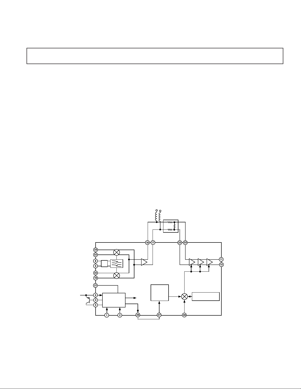
GENERAL DESCRIPTION
The AD6122 is a low power IF transmitter subsystem, specifically designed for CDMA applications. It consists of an I and Q
modulator, a divide-by-two quadrature generator, high dynamic
AD6122
range IF amplifiers with voltage-controlled gain and a powerdown control input. An integral low dropout regulator allows
operation from battery voltages from 2.9 V to 4.2 V.
The gain control input accepts an external gain control voltage
input from a DAC. It provides 97 dB of gain control with a
nominal 75 dB/V scale factor. Either an internal or an external
reference may be used to set the gain-control scale factor.
The I and Q modulator accepts differential quadrature baseband inputs from a CDMA baseband converter. The local oscillator is injected at twice the IF frequency. A divide-by-two
quadrature generator followed by dual polyphase filters ensures
±1° quadrature accuracy.
The modulator provides a common-mode reference output to
bias the transmit DACs in the baseband converter to the same
common-mode voltage as the modulator inputs, allowing dc
coupling between the two ICs and thus eliminating the need to
charge and discharge coupling capacitors. This allows the fastest
power-up and power-down times for the AD6122 and CDMA
baseband ICs.
The AD6122 is fabricated using a 25 GHz f
process and is packaged in a 28-lead SSOP and a 32-leadless
LPCC chip scale package (5 mm × 5 mm).
silicon BiCMOS
t
I INPUT
LOCAL
OSCILLATOR
INPUT
Q INPUT
COMMON-MODE
REFERENCE
OUTPUT
VPOS
FUNCTIONAL BLOCK DIAGRAM
QUADRATURE
MODULATOR
OUTPUT
QUADRATURE MODULATOR
ⴜ2
POWERDOWN 2
VREG
1.23 V
REFERENCE
OUTPUT
LOW
DROPOUT
REGULATOR
POWERDOWN 1
VCC
ATTENUATOR
AD6122
GAIN
CONTROL
SCALE
FACTOR
GAIN CONTROL
REFERENCE
VOLTAGE
INPUT
IF AMPLIFIER
INPUT
IF AMPLIFIERS
GAIN CONTROL
VOLTAGE
INPUT
TEMPERATURE
COMPENSATION
TRANSMIT
OUTPUT
REV. B
Information furnished by Analog Devices is believed to be accurate and
reliable. However, no responsibility is assumed by Analog Devices for its
use, nor for any infringements of patents or other rights of third parties
which may result from its use. No license is granted by implication or
otherwise under any patent or patent rights of Analog Devices.
One Technology Way, P.O. Box 9106, Norwood, MA 02062-9106, U.S.A.
Tel: 781/329-4700 World Wide Web Site: http://www.analog.com
Fax: 781/326-8703 © Analog Devices, Inc., 2000
Page 2

AD6122–SPECIFICATIONS
(TA = +25ⴗC, VCC = +3.0 V, LO = 2 ⴛ IF, REFIN = 1.23 V, LDO Enabled, unless otherwise
noted) NOTE: All powers shown in dBm are referred to 1 k⍀.
Specification Conditions Min Typ Max Unit
MODULATOR LO = 260.76 MHz (2 × IF), 100 mV p-p
500 mV p-p Differential I and Q Inputs;
Output Level Output Level Referred to a 1 kΩ Differential Load –21 dBm
Output Third Order Harmonic –50 dBc
I/Q Inputs
Differential Input Voltage Differential 500 mV p-p
Bandwidth –3 dB 20 MHz
Resistance 30 kΩ
Quadrature Accuracy ±1 °
Amplitude Balance ±0.1 dB
Output Referred Noise 0.9 MHz to 5.0 MHz Offsets –169 dBm/Hz
Modulator Common-Mode Reference 1.408 V
LO Input Resistance Differential Input at 260.38 MHz 1.2 kΩ
LO Input Capacitance Differential Input at 260.38 MHz 2.4 pF
LO Carrier Leakage Bias I/Q Using MODCMREF –40 dBc
IF AMPLIFIER F
Noise Figure VGAIN = 2.5 V, 1 kΩ Differential Load 10 dB
Input 1 dB Compression Point VGAIN = 2.5 V –32 dBm
Input Third-Order Intercept VGAIN = 2.5 V –24 dBm
Gain Flatness IF ±630 kHz ±0.25 dB
Input Capacitance Shunt Equivalent Model at 130.38 MHz 2.3 pF
Differential IF Input Resistance Shunt Equivalent Model at 130.38 MHz 680 Ω
Differential IF Output Resistance Per Pin at 130.38 MHz 4.2 kΩ
Differential IF Output Capacitance Per Pin at 130.38 MHz 2.0 pF
GAIN CONTROL INTERFACE
Gain Scaling Using Internal Reference 75 dB/V
Gain Scaling Linearity For a Typical Dynamic Range of 92 dB ±3 dB/V
Minimum Gain VGAIN = 0.5 V –63 dB
Maximum Gain VGAIN = 2.5 V +34 dB
Gain Control Response Time 90 dB Gain Change, Min Gain to Max Gain 0.7 µs
Input Resistance at REFIN 10 MΩ
Input Resistance at VGAIN 109 kΩ
POWER-DOWN INTERFACE
Logic Threshold High Power-Up on Logical High 1.34 V
Logic Threshold Low 1.30 V
Input Current for Logical High 0.1 µA
Turn-On Response Time Measure to Settling of AGC from Standby Mode 23 µs
Turn-Off Response Time To 200 µA Supply Current 187 ns
LOW DROPOUT REGULATOR External PNP Pass Transistor, VCE
Input Range 2.9–4.2 V
Nominal Output 2.70 V
Dropout Voltage 200 mV
Reference Output 1.23 V
POWER SUPPLY
Supply Range Bypassing Internal LDO 2.7–5.0 V
Supply Current VGAIN = 1.5 V (Unity Gain) 10.4 mA
Standby Current 7.8 µA
OPERATING TEMPERATURE
T
to T
MIN
Specifications subject to change without notice.
MAX
= 130.38 MHz
IF
Max, h
= 100/300 Min/Max
FE
= –0.4 V
SAT
–40 +85 °C
–2–
REV. B
Page 3
AD6122
WARNING!
ESD SENSITIVE DEVICE
ABSOLUTE MAXIMUM RATINGS
1
Supply Voltage DVCC, IFVCC, TXVCC to DGND,
IFGND . . . . . . . . . . . . . . . . . . . . . . . . . . . . . . . . . . . . +5 V
Internal Power Dissipation
2
. . . . . . . . . . . . . . . . . . . 600 mW
Operating Temperature Range . . . . . . . . . . . –40°C to +85°C
Storage Temperature Range . . . . . . . . . . . . –65°C to +150°C
Lead Temperature Range (Soldering 60 sec) . . . . . . . . +300°C
PIN CONFIGURATIONS
SSOP Package
PD1
PD2
LDOE
LDOB
LDOC
LDOGND
DGND
LOIPP
LOIPN
DVCC
TXOPP
TXOPN
TXVCC
IFGND
1
2
3
4
5
6
AD6122
7
TOP VIEW
(Not to Scale)
8
9
10
11
12
13
14
28
VGAIN
27
REFIN
26
REFOUT
25
IFVCC
24
IFGND
IIPP
23
22
IIPN
21
MODCMREF
QIPN
20
19
QIPP
18
MODOPP
17
MODOPN
16
IFINP
15
IFINN
NOTES
1
Stresses above those listed under Absolute Maximum Ratings may cause perma-
nent damage to the device. This is a stress rating only; functional operation of the
device at these or any other conditions above those indicated in the operational
section of this specification is not implied. Exposure to absolute maximum rating
conditions for extended periods may affect device reliability.
2
Thermal Characteristics: 28-lead SSOP Package: θJA = 115.25°C/W.
LPCC Package
REFIN
LDOB
LDOC
LDOGND
LDOGND
DGND
LOIPP
LOIPN
DVCC
VGAIN
PD1
PD2
LDOE
32
1
223
3
421
AD6122 Top View
5
619
7
8
(Not to Scale)
10311130122913281427152616
9
IFGND
IFGND
TXVCC
TXOPP
TXOPN
NC
IFVCC
REFOUT
25
24
IFGND
IFGND
22
IIPP
IIPN
20
MODCMREF
QIPN
QIPP
18
17
MODOPP
IFINP
IFINN
MODOPN
NC = NO CONNECT
ORDERING GUIDE
Temperature Package
Model Range Package Description Option
AD6122ARS –40°C to +85°C Shrink Small Outline Package (SSOP) RS-28
AD6122ARSRL –40°C to +85°C 28-Lead SSOP on Tape-and-Reel
AD6122ACP –40°C to +85°C Chip Scale Package (LPCC) CP-32
AD6122ACPRL –40°C to +85°C 32-Leadless LPCC on Tape-and-Reel
CAUTION
ESD (electrostatic discharge) sensitive device. Electrostatic charges as high as 4000 V readily
accumulate on the human body and test equipment and can discharge without detection.
Although the AD6122 features proprietary ESD protection circuitry, permanent damage may
occur on devices subjected to high-energy electrostatic discharges. Therefore, proper ESD
precautions are recommended to avoid performance degradation or loss of functionality.
REV. B
–3–
Page 4

AD6122
PIN FUNCTION DESCRIPTIONS
SSOP LPCC
Pin # Pin # Pin Label Description Function
1 30 PD1 Power-Down 1 IF Amplifier Power-Down Control Input; CMOS Com-
patible; HIGH = Entire IC Powers Down, LOW = IF
Amplifiers On.
2 31 PD2 Power-Down 2 Modulator Power-Down Control Input; CMOS Compat-
ible; HIGH = Modulator Off , LOW = Modulator On.
3 32 LDOE Low Dropout Regulator Pass Connects to Emitter of External PNP Pass Transistor
Transistor Emitter Connection and VCC.
4 1 LDOB Low Dropout Regulator Pass Connects to Base of External PNP Pass Transistor.
Transistor Base
5 2 LDOC Low Dropout Regulator Pass Connects to Collector of External PNP Pass Transistor.
Transistor Collector
6 3, 4 LDOGND Low Dropout Regulator Ground Ground.
7 5 DGND Digital Ground Ground.
8 6 LOIPP Local Oscillator “Positive” Input Connects to Local Oscillator; AC Coupled.
9 7 LOIPN Local Oscillator “Negative” Input Connects to Ground via Decoupling Capacitor.
10 8 DVCC Digital VCC Connects to Digital Supply.
11 9 TXOPP Transmit Output “Positive” Connects to Output Filter; AC Coupled.
12 10 TXOPN Transmit Output “Negative” Connects to Output Filter; AC Coupled.
13 11 TXVCC Transmit Output VCC Connects to LDO Output via Decoupling Network.
14 12, 13 IFGND IF Ground Ground.
15 14 IFINN IF Input “Negative” IF “Negative” Input from LC Roofing Filter.
16 15 IFINP IF Input “Positive” IF “Positive” Input from LC Roofing Filter.
17 16 MODOPN Modulator “Negative” If Output Output Modulator Output to LC Roofing Filter.
18 17 MODOPP Modulator “Positive” Output Modulator Output to LC Roofing Filter.
19 18 QIPP Q Input “Positive” Connects to Q “Positive” Output of Baseband IC.
20 19 QIPN Q Input “Negative” Connects to Q “Negative” Output of Baseband IC.
21 20 MODCMREF Modulator Common-Mode Connects to CDMA Baseband Converter Tx DAC
Reference Out Common-Mode Reference Input.
22 21 IIPN I Input “Negative” Connects to I “Negative” Output of Baseband IC.
23 22 IIPP I Input “Positive” Connects to I “Positive” Output of Baseband IC.
24 23, 24 IFGND Ground Connects to IF Ground.
25 NC No Connect
25 26 IFVCC IF VCC Connects to Decoupled Output of LDO Regulator.
26 27 REFOUT Gain Control Reference Output Provides 1.23 V Voltage Reference Output for DAC in
CDMA Baseband Converter and REFIN.
27 28 REFIN Gain Control Reference Input Accepts 1.23 V Reference Input from REFOUT or
External Reference.
28 29 VGAIN Gain Control Voltage Input Accepts Gain Control Input Voltage from External DAC.
Max Gain = 2.5 V; Min Gain = 0.5 V.
–4–
REV. B
Page 5
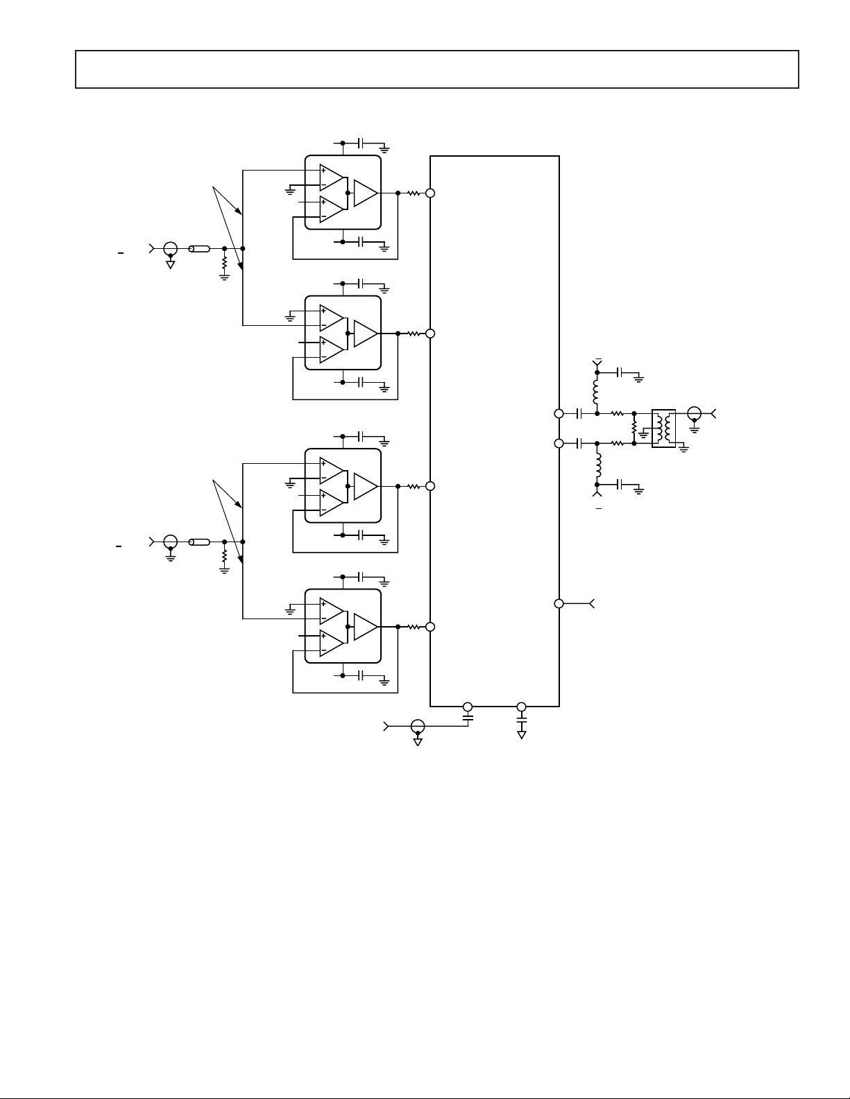
Test Figures
MUST BE EQUAL
LENGTHS
I DATA
MUST BE EQUAL
LENGTHS
Q DATA
50⍀
50⍀
MODCMREF
MODCMREF
MODCMREF
MODCMREF
AD6122
0.1F
+15V
8
V
X1
X2
Y1
Y2
–15V
+15V
X1
X2
Y1
Y2
–15V
+15V
X1
X2
Y1
Y2
–15V
+15V
X1
X2
Y1
Y2
–15V
V–1
V–1
V–1
V–1
V–1
V–1
V–1
V–1
P
V
N
5
8
V
P
V
N
5
8
V
P
V
N
5
8
V
P
V
N
5
OUT
A=1
AD830
0.1F
0.1F
OUT
A=1
AD830
0.1F
0.1F
OUT
A=1
AD830
0.1F
0.1F
OUT
A=1
AD830
0.1F
7
50⍀
IIPP
AD6122
7
7
7
50⍀
50⍀
50⍀
IIPN
QIPP
QIPN
LOIPP
MODOPP
MODOPN
LOIPN
VREG OUT
10nF
10nF
VREG OUT
MODCMREF
0.1F
450⍀
205⍀
450⍀
0.1F
MOD_OUT
1
2
3
4
1
2
3
4
1
2
3
4
1
2
3
4
REV. B
LO INPUT
Figure 1. Quadrature Modulator’s Characterization Input and Output Impedance Matches
–5–
Page 6
AD6122
VREG OUT
10nF
10nF
0.1F
453⍀
205⍀
453⍀
4:1
RF SOURCE
1:8
PULL-UP INDUCTORS CHOSEN
FOR PEAK RESPONSE AT THE
TEST FREQUENCY.
383⍀
511⍀
383⍀
IFINP TXOPP
10nF
IFINN
10nF
TXOPN
AD6122
0.1F
VREG OUT
Figure 2. IF Amplifier’s Characterization Input and Output Impedance Matches
NOTE: RF CABLES FOR I AND Q PATHS MUST BE OF EQUAL LENGTH
TEST BED MOTHERBOARD
I CHANNEL
Q CHANNEL
LO INPUT
IF IN
MOD OUT
IFTX OUT
TO RF SWITCHES
TEKTRONIX
AFG2002
R&S
SMT03
RF
RF SOURCE 1
I DATA
500mVp-p DIFFERENTIAL
Q DATA
RF
INPUT
TO
SPECTRUM
ANALYZER
R&S FSEA20/30
SPECTRUM
ANALYZER
AUX MEAS
PORT
R&S
SMT03
RF SOURCE 2
RF
HPE3610
POWER SUPPLY
Figure 3. General Test Set
HP34970A
DATA ACQUISITION
& SWITCH CONTROL
DC MEASUREMENTS
& CONTROL BITS
–6–
REV. B
Page 7

AD6122
HP8116A
FUNCTION GEN.
4kHz, 0V TO 2.7V
SQ. WAVE
ROHDE & SCHWARZ
SMT03
100kHz, –30dBm
AD6122 TEST BED
PD1,
PD2
IFIN
IFOUT
TEKTRONIX TDS 744A
CH 1 WITH X10 PROBE
CH 2 WITH COAX CABLE
50⍀
HP8116A
FUNCTION GEN.
4 kHz, 0.5V TO 2.5V
SQ. WAVE
AGC
AD6122 TEST BED
NOISE
SOURCE
ROHDE & SCHWARZ
100MHz, –30dBm
IFIN
IFOUT
REACTIVE
CONJUGATE
SMT03
VREG OUT
10nF
10nF
MATCH
1:8
PULL-UP INDUCTORS CHOSEN
FOR PEAK RESPONSE AT THE
TEST FREQUENCY.
IFINP TXOPP
10nF
IFINN
10nF
TXOPN
AD6122
VREG OUT
Figure 4. IF Amplifier’s Noise Figure Test Set
TEKTRONIX TDS 744A
CH 1 WITH X10 PROBE
CH 2 WITH COAX CABLE
50⍀
0.1F
453⍀
205⍀
453⍀
0.1F
4:1
TO NOISE
FILTER
METER
a. Response Time from Gain Control to IF Output
Figure 5. Response Time Setup
b. Response Time from PD1 and PD2 Control to IF Output
REV. B
–7–
Page 8

AD6122
–Typical Performance Characteristics
RBW
30kHz
VBW
REF LEV
–40dBm
–40
–50
–60
–70
–80
–90
–100
POWER – dBm
–110
–120
–130
–140
CL1
CENTER 130.38MHz 519kHz/DIV SPAN 5.19MHz
SWT
1
100kHz
2s
UNIT dBm
–49.18dBm
(T1)
1
130.67458918MHz
–33.92dBm
CH PWR
ACP UP
AVE LOW
–77.32dB
77.46dB
CU1
Figure 6. Spectral Plot at Modulator Outputs: ACPR
A
–30
–35
–40
UNDESIRED SIDEBAND – dBc
–45
50 350100
150 200 250 300
OUTPUT FREQUENCY – MHz
Figure 9. Modulator Output Undesired Sideband vs.
Output Frequency
–35
–40
–45
LO LEAKAGE – dBc
–50
50 350100
150 200 250 300
FREQUENCY – MHz
Figure 7. Modulator LO Leakage vs. Output Frequency
–15
–20
–25
–30
dBm REFERRED TO 1k⍀
–35
OUTPUT DESIRED SIDEBAND LEVEL –
–40
50 350100
150 200 250 300
OUTPUT FREQUENCY – MHz
Figure 8. Modulator Output Desired Sideband vs.
Output Frequency Without Roofing Filter
–10
–15
–20
–25
–30
TO A 1k⍀ DIFFERENTIAL LOAD
MODULATOR OUTPUT – dBm REFERRED
–35
–14.0 –2.0–12.0
–10.0 –8.0 –6.0 –4.0
MODULATOR, I = Q – dBV
Figure 10. Modulator Gain: Input (dBV) vs. Output (dBm)
–45
–50
–55
THIRD HARMONIC – dBc
–60
–65
50 350100
150 200 250 300
OUTPUT FREQUENCY – MHz
Figure 11. Modulator Third Harmonic
–8–
REV. B
Page 9

AD6122
–23
–26
50 350100
IIP3 – dBm Referred to 1k⍀
150 200 250 300
–24
–25
FREQUENCY – MHz
40
20
0
= +85ⴗC
T
A
TA = –40ⴗC
TA = +25ⴗC
1.5 2.0
VGAIN – V
–20
–40
GAIN – dB With a 1k⍀ Load
–60
–80
0.5 2.51.0
Figure 12. IF Amplifier Response Curve: Gain vs.
VGAIN, T
45
35
25
15
–5
–15
–25
GAIN – dB
–35
–45
–55
–65
–75
= –40°C, +25°C, +85°C
A
5
0.5 2.50.9
GAIN ERROR
GAIN
1.3 1.7 2.1
VGAIN – V
6.0
5.0
4.0
3.0
2.0
1.0
0
–1.0
–2.0
–3.0
–4.0
–5.0
–6.0
Figure 13. IF Amplifier Gain and Error vs. VGAIN
ERROR FROM PREDICTED VALVE – dB
–24
–25
–26
–27
IIP3 – dBm Referred to 1k⍀
–28
2.5 3.72.7
2.9 3.1 3.3 3.5
SUPPLY VOLTAGE – V
Figure 15. IF Amplifier Input IP3 vs. Supply Voltage
Figure 16. IF Amplifier Input IP3 vs. Frequency
5.0
0
–5.0
–10.0
–15.0
IIP3 – dBm Referred to 1k⍀
–20.0
–25.0
0.5 2.50.9
Figure 14. IF Amplifier Input IP3 vs. VGAIN
REV. B
1.3 1.7 2.1
VGAIN – V
–9–
30.0
25.0
20.0
15.0
NOISE FIGURE – dB
10.0
5.0
–10.0 40.00
313MHz
238MHz
10.0 20.0 30.0
GAIN – dB
133MHz
Figure 17. IF Amplifier Noise Figure vs. Gain
Page 10

AD6122
40
20
0
–20
GAIN – dB
–40
–60
–80
50 350100
VGAIN = 2.0V
VGAIN = 1.0V
VGAIN = 0.5V
150 200 250 300
FREQUENCY – MHz
VGAIN = 2.5V
VGAIN = 1.5V
Figure 18. IF Amplifier Gain vs. Frequency for
VGAIN = 2.5 V, 2.0 V, 1.5 V, 1.0 V
REF LEV
–30dBm
–30
–40
–50
–60
–70
–80
–90
POWER – dBm
–100
–110
–120
–130
CL1
CENTER 130.38MHz 600kHz/DIV SPAN 6MHz
Figure 20. ACPR of Cascaded Modulator, 20 dB Pad and IF
Amplifier: Spectral Plot
CO
RBW
VBW
SWT
1
18.0
16.0
14.0
12.0
10.0
TOTAL CURRENT CONSUMPTION – mA
8.0
0.5 2.5
1.0 1.5 2.0
VGAIN – V
Figure 19. Total Current Consumption vs. VGAIN
30kHz
300kHz
2s
UNIT dBm
–46.78dBm
(T1)
1
CO
1
130.38000000MHz
–31.93dBm
CH PWR
ACP UP
AVE LOW
(T1)
1
330.66132265kHz
CU1
–66.95dB
–68.95dB
–0.28 dB
A
–10–
REV. B
Page 11

I INPUT
LOCAL
OSCILLATOR
INPUT
QUADRATURE
MODULATOR
QUADRATURE MODULATOR
ⴜ2
OUTPUT
VCC
ATTENUATOR
IF AMPLIFIER
INPUT
IF AMPLIFIERS
TRANSMIT
OUTPUT
AD6122
1.23 V
AD6122
GAIN CONTROL
Q INPUT
COMMON-MODE
REFERENCE
OUTPUT
VPOS
LOW
DROPOUT
REGULATOR
POWERDOWN 1
POWERDOWN 2
VREG
REFERENCE
OUTPUT
Figure 21. Block Diagram
THEORY OF OPERATION
The CDMA Transmitter IF Subsystem (Figure 21) consists of
an I and Q modulator with a divide-by-two quadrature generator, high dynamic range IF amplifiers with voltage-controlled
gain, a low dropout regulator and power-down control inputs.
I and Q Modulator
The I and Q modulator accepts differential quadrature baseband
inputs from CDMA baseband converters. The LO is injected at
twice the IF frequency. A divide-by-two quadrature generator
followed by dual polyphase filters ensures ±1° quadrature accuracy (Figure 22).
For 500 mV p-p differential I and Q input signals, the output
power of the modulator will be –21 dBm referred to 1 kΩ when
the output of the modulator is loaded with a 1 kΩ differential
load. With the maximum input conditions stated above, the
modulator outputs are a 225 µA p-p differential current; conse-
quently, the output load will greatly affect the output power of
the modulator.
2 ⴛ IF
LO INPUT
180ⴗ
ⴜ2
ⴜ2
I
POLYPHASE
Q
FILTERS
I
QUADRATURE
OUTPUT TO
MODULATOR
Q
Figure 22. Simplified Quadrature Generator Circuit
The I and Q modulator also provides a common mode reference
signal at the MODCMREF pin. This voltage is a dc voltage set
to 1.408 V when a 2.7 V supply is used. It is used to dc bias
the output of the DAC that provides I and Q inputs to the
modulator.
GAIN
CONTROL
SCALE
FACTOR
REFERENCE
VOLTAGE
INPUT
GAIN CONTROL
VOLTAGE
INPUT
TEMPERATURE
COMPENSATION
IF Amplifiers and Gain Control
The IF amplifiers provide an 86 dB linear in dB gain control
range. The input stage uses a differential, continuously variable
attenuator based on Analog Devices’ patented X-AMP™ topology. This low noise attenuator consists of a differential R-2R
ladder network, linear interpolator and a fixed gain amplifier.
The IF amplifier’s input impedance is 1 kΩ differential. Similar
to the I and Q modulator’s output, the IF amplifier’s output is a
differential current, which will vary depending upon the gain
control voltage. In order to achieve the specified gain, the output of the IF amplifiers should be loaded with a 1 kΩ differential load.
The gain control circuits contain both temperature compensation circuitry and a choice of internal or external reference for
adjusting the gain scale factor. The gain control input accepts
an external gain control voltage input from a DAC. It provides
97 dB of gain control range with a nominal 75 dB/V scale factor.
The external gain control input signal should be a clean signal.
It is recommended to filter this signal in order to eliminate the
noise that results from the DAC. If a noisy signal is used for the
gain control voltage, VGAIN inband and adjacent channel noise
peaking can occur at the output of the AD6122. A simple RC
filter can be employed, but care should be taken with its design.
If too big a resistor is used, a large voltage drop may occur
across the resistor, resulting in lower gain than expected (as a
result of a lower voltage reaching the AD6122). An RC filter
with a 20 kHz bandwidth, employing a 1 kΩ resistor is appropriate. This results in an 8.2 nF capacitor. The resulting circuit
is shown in Figure 23. Note that the input resistance at the
VGAIN pin is approximately 100 kΩ.
FROM
BASEBAND
CONVERTER
1k⍀
8.2nF
AD6122
VGAIN
109k⍀
X-AMP is a trademark of Analog Devices, Inc.
REV. B
Figure 23. Gain Voltage Filtering
–11–
Page 12

AD6122
The AD6122’s overall gain, expressed in decibels, is linear in
dB with respect to the automatic gain control (AGC) voltage,
VGAIN. Either REFOUT or an external reference voltage connected to REFIN may be used to set the voltage range for VGAIN.
When the internal 1.23 V reference, REFOUT, is connected to
REFIN , VGAIN will control the entire AGC range when it is
typically set between 0.5 V and 2.5 V. Minimum gain occurs at
minimum voltage on VGAIN and maximum gain occurs at maximum voltage on VGAIN. The maximum and minimum gain
will not change with a change in voltage at REFIN. Rather, the
slope of the gain curve will change as a result of a change in the
required range for VGAIN. Figure 24 shows the piecewise linear
approximation of the gain curve for the AD6122.
MAXIMUM
GAIN
GAIN – V/V
MINIMUM
GAIN
VGAIN – V
Figure 24. Piecewise Linear Approximation for the
AD6122 Gain Curve
Because the minimum and maximum gain from the AD6122
are constant, we can approximate the VGAIN range for a
given REFIN voltage by using Equation 1.
VGAIN
GAIN MinGain REFIN
( – ).
MaxGain MinGain
×
–
REFIN=
+
.1604
(1)
Where MaxGain is the maximum gain (+34 dB) in dB, MinGain
is the minimum gain (–63 dB) in dB, REFIN is the reference
input voltage, in volts, VGAIN is the gain control voltage input,
in volts, and GAIN is the particular gain, in dB, we would have
for a given REFIN and VGAIN. Consequently, for any REFIN
we choose, we can calculate the VGAIN range by solving
Equation 1 for VGAIN. For example, in order to determine the
VGAIN value for the maximum gain condition, given a 1.23 V
REFIN, we can solve Equation 1 for VGAIN by substituting
+34 dB for GAIN and MaxGain, –63 dB for MinGain and 1.23 V
for REFIN. VGAIN can then be calculated to be 2.46 V, or
approximately 2.5 V. For the minimum gain condition, we can
determine the VGAIN value by substituting 34 dB for MaxGain,
–63 dB for GAIN and MinGain and 1.23 V for REFIN. VGAIN
can then be calculated to be 0.492 V or approximately 0.5 V.
Power-Down Control
The AD6122 can be operated with the IF amplifiers and quadrature modulator both powered up, both powered down or with
the IF amplifiers powered up and the modulator powered down.
The AD6122 cannot operate with only the modulator powered
up. The control is provided via two control pins, PD1 and PD2.
Table I shows the operating modes of the AD6122.
Table I. Operating Modes
PD1 PD2 IF Amp Modulator
0 0 ON ON
0 1 ON OFF
1 0 INVALID STATE INVALID STATE
1 1 OFF OFF
Low Dropout Regulator
The AD6122 incorporates an integrated low dropout regulator.
The regulator accepts inputs from 2.9 V to 4.2 V and supplies a
constant 2.7 V reference output at LDOC. The 2.7 V signal can
be used to provide the dc voltages required for the DVCC,
TXVCC and IFVCC dc supplies. In order to configure the low
dropout regulator, an external pass transistor is required. A pnp
bipolar junction transistor with a minimum h
maximum h
of 300 and a VCE
FE
of –0.4 V is required. In
SAT
of 100 and a
FE
order to use the low dropout regulator, configure the transistor as
shown in Figure 25. The 18 pF capacitor in Figure 25 is used for
decoupling the 2.7 V dc signal.
In addition to the low dropout regulator, a band-gap voltage
reference produces a 1.23 V reference voltage at REFOUT.
This reference voltage will be present whenever a 2.7 V dc signal is present on pin LDOC. This 1.23 V reference voltage can
then be used to provide the gain reference signal required for
REFIN and the reference voltage for the transmit DACs in a
baseband converter.
AD6122
2.9V – 4.2V
2.7V
PASS
TRANSISTOR
18pF
LDOE
LDOB
LDOC
REFOUT
1.23V
Figure 25. Configuring the Low Dropout Regulator
It is possible to bypass the low dropout regulator on the AD6122
and use an external regulator instead. In order to bypass the
integrated low dropout regulator, connect pins LDOE, LDOB
and LDOC together and then connect them all to the 2.7 V
external regulator voltage. This configuration is shown in
Figure 26. Even when the low dropout regulator is bypassed,
the 1.23 V reference voltage at pin REFOUT is still present.
–12–
REV. B
Page 13

AD6122
AD6122
LDOE
FROM EXTERNAL
VOLTAGE REGULATOR
LDOB
LDOC
REFOUT
1.23V
Figure 26. Configuration for Bypassing the Low Dropout
Regulator
ROOFING FILTER
Because the outputs of the AD6122 modulator are open collector, the parasitic capacitances seen at the output of the modulator, and inputs of the IF amplifiers, are high enough to create a
low-pass filter, which may attenuate the IF signal. Consequently,
the parasitic capacitance must be cancelled by using external
inductors to form a parallel resonant circuit. The external inductors and the internal parasitic capacitors form what is known
as the roofing filter, with the resonant frequency given by
Equation 2.
1
LC
2=π
is the IF frequency, in Hertz, C
0
PAR
is the total parasitic
PAR
(2)
where f
f
0
capacitance in Farads, and L is the value of external inductors,
in henrys.
The roofing filter may be composed of the pull-up inductors
required on the open collector outputs of the I and Q modulator. This configuration is shown in Figure 27. The 10 nF capacitors are used for ac coupling.
AD6122
MODOPP
2C
PAR
2C
PAR
MODOPN
IFINN
IFINP
L/2
L/2
VCC
PARALLEL
RESONANT
CIRCUIT
10nF
10nF
10nF
ATTENUATOR
Figure 27. Roofing Filter Configuration
The attenuator is discussed in the next section entitled Measuring Adjacent Channel Protection Ratio (ACPR).
In order to confirm whether the roofing filter has been correctly
designed, sweep the LO frequency and view the output of the IF
amplifier on a spectrum analyzer. The signal should peak at the
IF frequency if the inductor value is correct. The Q of the filter
should be low enough so that variations in the parasitic capacitances should be negligible.
The value of inductor required will be a function of the IF frequency at which we are operating. The values of inductors used
during characterization at Analog Devices are shown in Table
II. Because the exact value will also be a function of printed
circuit board layout, we will have to vary the value from those in
Table II to those required for our board.
Table II. Roofing Filter Inductor Values
Value of Roofing Filter
IF Frequency (MHz) Inductor (nH)
50–125 470
126–200 150
201–275 68
276–350 27
It should be noted that the roofing filter is only required when
cascading the output from the I/Q modulator to the input of the
IF amplifiers. If we are driving into the IF amplifiers directly, no
roofing filter is required, however, pull-up inductors are required
in order to set the dc voltage of the open collector modulator
outputs.
MEASURING ADJACENT CHANNEL POWER RATIO
(ACPR)
At maximum IF gain and specified input conditions (500 mV
p-p baseband inputs), the output of the I/Q modulator is 11 dB
greater than the P1 dB (one dB compression point) of the IF
amplifiers. This configuration maximizes the ratio of signal to
LO feedthrough and also maximizes the signal to noise ratio.
Once these ratios are maximized, we can attenuate the noise,
signal and LO feedthrough without affecting the ratios. Therefore, attenuation is required between the I/Q modulator and the
IF amplifiers.
In order to determine exactly how much attenuation is required,
we must recognize that ACPR is a function of the attenuation
from the modulator outputs to the IF amplifier inputs. As a
result, in order to determine how much attenuation is required,
we must first know how good an ACPR performance is desired.
If too much attenuation is applied, the ACPR will be very good,
but, the IF amplifier’s output power level will be low, possibly
resulting in poor signal to noise ratio and possibly requiring
additional amplification external to the AD6122.
An appropriate method that can be used to provide the correct
amount of attenuation between the modulator outputs and the
IF amplifier inputs is a simple differential voltage divider. The
topology and its design equations are shown in Figure 28 and
Equations 3 and 4. The input impedance of the IF amplifiers is
typically 1 kΩ. As a result, if we design resistor R2 to be much
less than 1 kΩ, we can neglect the effects of the IF amplifier’s
input impedance on the attenuator.
REV. B
–13–
Page 14

AD6122
AD6122
MODOPP
Z
IN
MODOPN
R1
R2
R1
Figure 28. Pad Topology
20
log
L
=
ZRR
IN
111
RR
=+21 2
1
1
R
+
22
/
where L is the transducer loss (or loss through the pad) in dB
and Z
is the desired input resistance in ohms. Using these
IN
equations, we can design the attenuator circuit to provide whatever amount of attenuation we require.
IFINP
RSHUNT >>R2
IFINN
(3)
(4)
This circuit is very sensitive to parasitic capacitances. As a result, extra care should be taken to ensure minimum and equal
printed circuit board transmission lines. We should also try to
keep R2 small in order to minimize the effects of printed circuit
board parasitic capacitance on loading the output of the pad.
In conclusion, we have to develop a system-level ACPR budget
for our radio, and from that budget determine how much ACPR
performance we desire from the AD6122. We then need to implement the appropriate attenuation network to get that ACPR
performance.
LEVEL DIAGRAM
Figure 29 is provided to better understand the different voltage
levels you can expect to see at different points of the AD6122. It
represents the voltage and power levels expected for a maximum
input condition of 500 mV p-p at the I and Q modulator and
maximum gain in the IF amplifiers. When trying to make these
measurements, a high impedance (10 MΩ) active FET probe
(for example, the Tek P6204, from Tektronix) should be used to
minimize the effects of loading the circuit with the probe.
In order to produce these results, the attenuator is designed to
have a 1 kΩ input impedance and the output of the IF amplifiers
are loaded with 1 kΩ. The roofing filter is designed to resonate
the parasitic capacitance at the IF frequency.
I
500mV p-p
DIFFERENTIAL
ⴜ2
LO
100mV p-p
DIFFERENTIAL
Q
500mV p-p
DIFFERENTIAL
MODULATORS
–21dBm
(REFERRED TO 1k⍀)
252.1mV p-p DIFFERENTIAL
Z
= 1k⍀
IN
MODOP
VCC
20dB
ATTENUATOR
Figure 29. Level Diagram
–41dBm
(REFERRED TO 1k⍀)
25.21mV p-p
DIFFERENTIAL
IFIN
IF AMPLIFIERS
VGAIN = 2.5V
GAIN = +34dB
–7dBm
(REFERRED TO 1k⍀)
1.263V p-p DIFFERENTIAL
TRANSMIT
OUTPUT
Z
= 1k⍀
OUT
1k⍀
–14–
REV. B
Page 15

INPUT INTERFACES
The AD6122 interfaces to CDMA baseband converters providing either IF or baseband outputs. The baseband input is provided by direct connection of the baseband converter’s baseband
output to the baseband input of the AD6122 (Figure 30). The
IF amplifier’s gain control is provided by connection of the
transmit AGC DAC’s output on the baseband converter, through a
low-pass filter to the VGAIN pin on the AD6122.
AD6122
VCC
PD1
PD2
LDOE
LDOB
LDOC
LDOGND
DGND
LOIPP
LOIPN
DVCC
TXOPP
TXOPN
TXVCC
IFGND
TEMPERATURE
COMPENSATION
LOW
DROPOUT
REGULATOR
ⴜ2
AD6122
GAIN
CONTROL
SCALE
FACTOR
Q
I
VGAIN
REFIN
REFOUT
IFVCC
IFGND
IIPP
IIPN
MODCMREF
QIPN
QIPP
MODOPP
MODOPN
VCC
IFINP
IFINN
VCC
TX AGC DAC
REF IN
EXT
OUTPUT
I
OUTPUT
I
VCM REF IN
OUTPUT
Q
Q
OUTPUT
CDMA
BASEBAND
IC
REV. B
Figure 30. Typical Connections to Baseband IC Using I and Q Inputs with SSOP Package
–15–
Page 16

AD6122
AD6122 Evaluation Board
The AD6122 Evaluation Board consists of an AD6122, I/O connectors, a 20-pin dual header, 2-pin headers and four AD830
high speed video difference amplifiers. It allows the user to
evaluate the AD6122’s IF amplifier and modulator together or
separately. Because the AD6122 may be used at any IF from 50
MHz to 350 MHz, pads are provided on the LOIPP input,
TXOP output, MODOP output and IFIP inputs to allow the
user to add matching networks. The board is configured for an
IF frequency of 130.38 MHz when shipped. There is no difference between the configuration of the boards with the SSOP or
LPCC package.
The AD830s are used to provide single-ended to differential
conversion and the appropriate phase shift for the I and Q data
input pins. As a result, a single-ended signal generator can be
used to generate these signals.
In order to test the power-down modes of the AD6122, locate
the two pin headers on the AD6122 evaluation boards labeled
PD1 and PD2. By open-circuiting the pins labeled PD1, the IF
amplifiers power down. By open-circuiting the pins labeled
PD2, the modulator powers down. Note that the IF amplifiers
and modulator are powered down unless the pins on the two pin
headers, PD1 and PD2, are short circuited.
The IF input port impedance match used during characterization of the AD6122 at Analog Devices is as follows:
50⍀
SIGNAL
GENERATOR
1:8
383⍀
511⍀
383⍀
1k⍀
AD6122
IFINP
IFINN
Figure 31. IF Input Port Impedance Match Used During
Characterization at ADI
This is a broadband lossy match used for characterization over
the 50 MHz to 350 MHz frequency range. All dBm references
in the characterization data collected using this match are referenced to 1 kΩ. Note that the 1:8 ratio in Figure 31 is an impedance ratio and not a voltage ratio.
The IF output port impedance match used during characterization at Analog Devices is as follows:
AD6122
TXOPP
TXOPN
1k⍀
453⍀
205⍀
453⍀
4:1
50⍀
SPECTRUM
ANALYZER
Figure 32. IF Output Port Impedance Match Used During
Characterization at ADI
This is a broadband lossy output match for the 50 MHz to
350 MHz frequency range. The 4:1 ratio in Figure 32 is an
impedance ratio and not a voltage ratio.
As shipped, the board is configured as follows:
1. J1 is open and J2 is shorted. This enables the LDO regulator.
The external PNP transistor should remain in place even
when the regulator is bypassed (the Pin LDOB is pulled up
by the transistor).
2. X11, X25, X18 and X26 are shorted and X12, X14, X19
and X21 are opened in order to connect the output of the
modulator to the input of the IF amplifiers.
3. L4 and L5, the roofing filter components are optimized for
an IF frequency of 130.38 MHz.
4. R14, R15 and R16 set the attenuation between the modulator outputs and the IF amplifier inputs to 20 dB.
5. PD1 and PD2 are pulled low by the jumpers on the two pin
headers. To power down the chip, set PD1 and PD2 high by
removing the jumpers.
In order to look at the modulator and IF amplifiers separately,
disconnect the output of the modulator from the input of the IF
amplifiers. This is accomplished by short circuiting X12, X14,
X19 and X20 and open circuiting X11, X18, X25 and X26.
–16–
REV. B
Page 17

AD6122
Table III describes the high frequency signal connectors on the
AD6122 customer sample boards.
Table III. Evaluation Board SMA Signal Connector
Description
Connector Description
I CH I Modulator Input. 250 mV p-p into 50 Ω
termination, dc coupled. The level shifting and
phase splitting is done on board by the AD830
amplifiers.
Q CH Q Modulator Input. 250 mV p-p into 50 Ω
termination, ac coupled. The level shifting and
phase splitting is done on board by the AD830
amplifiers.
MODOP Modulator Output. The differential-to-single
ended conversion is performed by a balun on
the board. Impedance matched to 50 Ω for
130.38 MHz IF frequency.
IFIP IF Amplifier Input. Single-ended-to-differential
conversion performed by a balun on board.
Impedance matched to 50 Ω for 130.38 MHz IF
frequency.
TXOP IF Amplifier Output. Differential-to-single-
ended conversion performed by a balun on
board. Impedance matched to 50 Ω for 130.38
MHz IF frequency.
LOIPP Local oscillator positive input at 2 × IF
frequency.
Table IV lists the connections for the 20-pin power-supply
connector.
Table IV. 20-Pin Power Supply Connection Information
Pin # Function
1 VPOS for AD6122; 2.9 V to 4.2 V using regulator; 2.7 V
to 4.2 V bypassing regulator.
2 VPOS for AD6122; 2.9 V to 4.2 V using regulator; 2.7 V
to 3.6 V bypassing regulator.
3 Ground.
4 Ground.
5 Ground.
6 Regulated Output or Input Voltage; Connects to Pin 5
on AD6122.
7 Ground.
8 Ground.
9 Ground.
10 Ground.
11 Ground.
12 PD1; Power-Down 1 Input.
13 Ground.
14 1.23 V Reference Voltage from AD6122.
15 Ground.
16 VGAIN; Gain Control Voltage Input.
17 –15 V Supply for AD830 Differential Amplifier.
18 +15 V Supply for AD830 Differential Amplifier.
19 MODCMREF; common-mode reference output for
baseband converter common-mode reference input.
20 PD2; Power-Down 2 Input.
A schematic diagram of the evaluation board is on the next two
pages.
REV. B
–17–
Page 18

AD6122
LOIPP
TXOP
VPOS
2.9V – 4.2V
VREG OUT
100nH
X4
AD6122
PD1
Q1
L2
220nH
L3
220nH
C25
10nF
C2
10nF
DVCC
TXVCC
PD2
C23
18pF
J2
0⍀
FMMT4403CT-ND
J1
C1
X2
10nF
0⍀
X7
X10
X8
0⍀
0⍀
0.1F
VCC
C24
10nF
10nF
VCC
C3
X9
C4
X1
X3
X5
X6
3pF
1:8
T1
PD1
PD2
LDOE
LDOB
LDOC
LDOGND
DGND
LOIPP
LOIPN
DVCC
TXOPP
TXOPN
TXVCC
IFGND
VGAIN
REFIN
REFOUT
IFVCC
IFGND
IIPP
IIPN
MODCMREF
QIPN
QIPP
MODOPP
MODOPN
IFINP
IFINN
R14 = 442⍀
R15 = 100⍀
R16 = 442⍀
R12
0⍀
IFVCC
MODCMREF
C10
10nF
C11
10nF
IIPP
IIPN
QIPN
QIPP
C8
10nF
X11
R14
X18
0⍀
0⍀
C28
10nF
C29
10nF
VREG
C9
10nF
L6
C30
R13
R15
VGAIN
REFOUT
OUT
C27
10nF
L4
180nH
X12
R16
X26
0⍀
X14
X25
0⍀
X19
X21
VREG
X13
X20
OUT
C26
10nF
L5
180nH
T2
8:1
X16
100nH
X15
4pF
8:1
X22
56nH
T3
X23
27nH
MODOP
X17
IFIP
X24
Figure 33. Schematic Diagram of the Evaluation Board
–18–
REV. B
Page 19

AD6122
ICH
C15
–15V
–15V
V–1
V–1
V–1
V–1
R1
10⍀
C13
0.01F
R2
10⍀
C12
0.01F
R3
10⍀
C14
0.01F
0.1F
8
A=1
AD830
5
C16
0.1F
C17
0.1F
8
A=1
AD830
5
C18
0.1F
U2
U3
SOIC PACKAGE
R7
50⍀
7
R8
50⍀
7
OUT
VREG
MODCMREF
+15V
1
2
C6
18pF
C5
18pF
C7
18pF
3
4
+15V
1
2
3
4
MODCMREF
R6
50⍀
MODCMREF
TO
TXVCC
TO
DVCC
TO
IFVCC
NOTES:
1. TO USE THE LDO REGULATOR, SHORT J2 AND OPEN J1.
2. TO BYPASS THE REGULATOR, SHORT J1 AND OPEN J2
3. TO CONNECT THE OUTPUT OF THE MODULATOR TO THE
INPUT OF THE IF AMP, SHORT J5 AND J6.
TO TEST THE MODULATOR AND THE IF AMP SEPARATELY,
OPEN J5 AND J6.
4. INDICATES A 50⍀ TRACE.
TO
IIPP
TO
IIPN
–15V
QCH
C19
+15V
1
2
MODCMREF
R9
50⍀
MODCMREF
P1
1
3
5
7
9
11
13
15
17
19
VPOS
P2
2
4
6
8
10
12
14
16
18
20
3
4
1
2
3
4
470nH
VREG
PD1
REFOUT
VGAIN
+15V
PD2
+15V
L1
0.1F
8
V–1
V–1
AD830
5
–15V
0.1F
0.1F
8
V–1
V–1
AD830
5
–15V
0.1F
OUT
PD1 PD2
SOIC PACKAGE
U4
7
A=1
C20
C21
U5
7
A=1
C22
R4
10k⍀R510k⍀
R10
50⍀
TO
QIPP
R11
50⍀
TO
QIPN
FROM VPOS
2.9V–4.2V
REV. B
Figure 34. Schematic Diagram of the Evaluation Board
–19–
Page 20

AD6122
OUTLINE DIMENSIONS
Dimensions shown in inches and (mm).
28-Lead SSOP
(RS-28)
0.407 (10.34)
0.397 (10.08)
28 15
0.311 (7.9)
0.301 (7.64)
0.078 (1.98)
0.068 (1.73)
0.008 (0.203)
0.002 (0.050)
0.010
(0.25)
REF
0.212 (5.38)
0.205 (5.21)
141
PIN 1
0.0256
(0.65)
BSC
0.015 (0.38)
0.010 (0.25)
0.066 (1.67)
SEATING
PLANE
0.07 (1.79)
0.009 (0.229)
0.005 (0.127)
8°
0°
0.03 (0.762)
0.022 (0.558)
32-Leadless Chip Scale Package (LPCC)
(CP-32)
0.205 (5.20)
0.197 (5.00) SQ
0.189 (4.80)
0.020 (0.50)
BSC
CONTROLLING DIMENSIONS ARE IN MILLIMETERS
0.002 (0.05)
0.001 (0.02)
0.000 (0.00)
DIMENSIONS MEET JEDEC MO-220-VHHD-2
0.128 (3.25)
0.106 (2.70) SQ
0.049 (1.25)
25
24
BOTTOM
VIEW
17
16
0.138 (3.50) BSC
0.039 (1.00)
0.035 (0.90)
0.031 (0.80)
32
1
8
9
PIN 1
INDICATOR
0.015 (0.38)
0.012 (0.30)
0.009 (0.23)
0.018 (0.45)
0.016 (0.40)
0.014 (0.35)
C00946a–.5–6/00 (rev. B)
–20–
PRINTED IN U.S.A.
REV. B
 Loading...