

Page 1

Low Power Mixer
a
FEATURES
Complete Receiver-on-a-Chip: Monoceiver
–15 dBm 1 dB Compression Point
–8 dBm Input Third Order Intercept
500 MHz RF and LO Bandwidths
Linear IF Amplifier
Linear-in-dB Gain Control
Manual Gain Control
Quadrature Demodulator
On-Board Phase-Locked Quadrature Oscillator
Demodulates IFs from 1 MHz to 12 MHz
Can Also Demodulate AM, CW, SSB
Low Power
25 mW at 3 V
CMOS Compatible Power-Down
APPLICATIONS
GSM and TETRA Receivers
Satellite Terminals
Battery-Powered Communications Receivers
®
Mixer
3 V Receiver IF Subsystem
AD61009
PIN CONFIGURATION
20-Lead SSOP
(RS Suffix)
FDIN
COM1
PRUP
LOIP
RFLO
RFHI
GREF
MXOP
VMID
IFHI
1
2
3
4
5
AD61009
TOP VIEW
6
(Not to Scale)
7
8
9
10
20
VPS1
19
FLTR
18
IOUT
17
QOUT
16
VPS2
15
DMIP
14
IFOP
13
COM2
12
GAIN
11
IFLO
GENERAL DESCRIPTION
The AD61009 is a 3 V low power receiver IF subsystem for operation at input frequencies as high as 500 MHz and IFs from
400 kHz to 12 MHz. It consists of a mixer, IF amplifiers, I and
Q demodulators, a phase-locked quadrature oscillator, and a
biasing system with external power-down.
The AD61009’s low noise, high intercept mixer is a doublybalanced Gilbert cell type. It has a nominal –15 dBm input
referred 1 dB compression point and a –8 dBm input referred
third-order intercept. The mixer section of the AD61009 also
includes a local oscillator (LO) preamplifier, which lowers the
required LO drive to –16 dBm.
In MGC operation, the AD61009 accepts an external gaincontrol voltage input from an external AGC detector or a DAC.
Monoceiver is a registered trademark of Analog Devices, Inc.
A quadrature VCO phase-locked to the IF drives the I and Q
demodulators. The I and Q demodulators can also demodulate AM; when the AD61009’s quadrature VCO is phase locked
to the received signal, the in-phase demodulator becomes a
synchronous product detector for AM. The VCO can also be
phase-locked to an external beat-frequency oscillator (BFO),
and the demodulator serves as a product detector for CW or
SSB reception. Finally, the AD61009 can be used to demodulate BPSK using an external Costas Loop for carrier recovery.
REV. 0
Information furnished by Analog Devices is believed to be accurate and
reliable. However, no responsibility is assumed by Analog Devices for its
use, nor for any infringements of patents or other rights of third parties
which may result from its use. No license is granted by implication or
otherwise under any patent or patent rights of Analog Devices.
One Technology Way, P.O. Box 9106, Norwood, MA 02062-9106, U.S.A.
Tel: 781/329-4700 World Wide Web Site: http://www.analog.com
Fax: 781/326-8703 © Analog Devices, Inc., 2001
Page 2

AD61009–SPECIFICATIONS
(@ TA = 25ⴗC, Supply = 3.0 V, IF = 10.7 MHz, unless otherwise noted)
Model AD61009ARS
Conditions Min Typ Max Unit
DYNAMIC PERFORMANCE
MIXER
Maximum RF and LO Frequency Range For Conversion Gain > 20 dB 500 MHz
Maximum Mixer Input Voltage For Linear Operation; Between RFHI and RFLO ± 54 mV
Input 1 dB Compression Point RF Input Terminated in 50 Ω –15 dBm
Input Third-Order Intercept RF Input Terminated in 50 Ω –5 dBm
Noise Figure Matched Input, Max Gain, f = 83 MHz, IF = 10.7 MHz 14 dB
Matched Input, Max Gain, f = 144 MHz, IF = 10.7 MHz 12 dB
Maximum Output Voltage at MXOP Z
Mixer Output Bandwidth at MXOP –3 dB, Z
= 165 Ω, at Input Compression ± 1.3 V
IF
= 165 Ω 45 MHz
IF
LO Drive Level Mixer LO Input Terminated in 50 Ω –16 dBm
LO Input Impedance LOIP to VMID 1 kΩ
Isolation, RF to IF RF = 240 MHz, IF = 10.7 MHz, LO = 229.3 MHz 30 dB
Isolation, LO to IF RF = 240 MHz, IF = 10.7 MHz, LO = 229.3 MHz 20 dB
Isolation, LO to RF RF = 240 MHz, IF = 10.7 MHz, LO = 229.3 MHz 40 dB
Isolation, IF to RF RF = 240 MHz, IF = 10.7 MHz, LO = 229.3 MHz 70 dB
IF AMPLIFIERS
Noise Figure Max Gain, f = 10.7 MHz 17 dB
Input 1 dB Compression Point IF = 10.7 MHz –15 dBm
Output Third-Order Intercept IF = 10.7 MHz 18 dBm
Maximum IF Output Voltage at IFOP Z
= 600 Ω±560 mV
IF
Output Resistance at IFOP From IFOP to VMID 15 Ω
Bandwidth –3 dB at IFOP, Max Gain 45 MHz
GAIN CONTROL (See Figures 10 and 11)
Gain Control Range Mixer + IF Section, GREF to 1.5 V 90 dB
Gain Scaling GREF to 1.5 V 20 mV/dB
GREF to General Reference Voltage V
R
75/V
R
dB/V
Gain Scaling Accuracy GREF to 1.5 V, 80 dB Span ± 1dB
Bias Current at GAIN 5 µA
Bias Current at GREF 1 µA
Input Resistance at GAIN, GREF 1MΩ
I AND Q DEMODULATORS
Required DC Bias at DMIP VPOS/2 V dc
Input Resistance at DMIP From DMIP to VMID 50 kΩ
Input Bias Current at DMIP 2 µA
Maximum Input Voltage IF > 3 MHz ±150 mV
IF ≤ 3 MHz ±75 mV
Amplitude Balance IF = 10.7 MHz, Outputs at 600 mV p-p, F = 100 kHz ± 0.2 dB
Quadrature Error IF = 10.7 MHz, Outputs at 600 mV p-p, F = 100 kHz –3.5 –1.2 +1.5 Degrees
Phase Noise in Degrees IF = 10.7 MHz, F = 10 kHz –100 dBc/Hz
Demodulation Gain Sine Wave Input, Baseband Output 17.4 18 18.8 dB
Maximum Output Voltage R
Output Offset Voltage Measured from I
≥ 20 kΩ±1.23 V
L
OUT
, Q
to VMID –100 10 +100 mV
OUT
Output Bandwidth Sine Wave Input, Baseband Output 1.5 MHz
PLL
Required DC Bias at FDIN VPOS/2 V dc
Input Resistance at FDIN From FDIN to VMID 50 kΩ
Input Bias Current at FDIN 200 nA
Frequency Range 1.0 to 12 MHz
Required Input Drive Level Sine Wave Input at Pin 1 400 mV
Acquisition Time to ± 3° IF = 10.7 MHz 16.5 µs
POWER-DOWN INTERFACE
Logical Threshold For Power Up on Logical High 2 V dc
Input Current for Logical High 75 µA
Turn-On Response Time To PLL Locked 16.5 µs
Standby Current 550 µA
POWER SUPPLY
Supply Range 2.85 5.5 V
Supply Current 8.5 12.5 mA
OPERATING TEMPERATURE
T
MIN
to T
MAX
Operation to 2.85 V Minimum Supply Voltage –25 +85 °C
Operation to 4.5 V Minimum Supply Voltage –40 +85 °C
Specifications subject to change without notice.
–2–
REV. 0
Page 3

AD61009
ABSOLUTE MAXIMUM RATINGS
Supply Voltage VPS1, VPS2 to COM1, COM2 . . . . . . . 5.5 V
Internal Power Dissipation
2
. . . . . . . . . . . . . . . . . . . . 600 mW
1
2.7 V to 5.5 V Operating Temperature Range
. . . . . . . . . . . . . . . . . . . . . . . . . . . . . . . . . . . –25°C to +85°C
4.5 V to 5.5 V Operating Temperature Range
NOTES
1
Stresses above those listed under Absolute Maximum Rating may cause permanent
damage to the device. This is a stress rating only; functional operation of the device
at these or any other conditions above those indicated in the operational section
of this specification is not implied. Exposure to absolute maximum rating conditions for extended periods may affect device reliability.
2
Thermal Characteristics: 20-lead SSOP Package: θJA = 126°C/W.
. . . . . . . . . . . . . . . . . . . . . . . . . . . . . . . . . . . – 40°C to +85°C
Storage Temperature Range . . . . . . . . . . . . –65°C to +150°C
Lead Temperature Range (Soldering 60 sec) . . . . . . . . . 300°C
CAUTION
ESD (electrostatic discharge) sensitive device. Electrostatic charges as high as 4000 V readily
accumulate on the human body and test equipment and can discharge without detection.
WARNING!
Although the AD61009 features proprietary ESD protection circuitry, permanent damage may
occur on devices subjected to high-energy electrostatic discharges. Therefore, proper ESD
precautions are recommended to avoid performance degradation or loss of functionality.
ESD SENSITIVE DEVICE
ORDERING GUIDE
Model Temperature Range Package Description Package Option
AD61009ARS –25°C to +85°C for 2.7 V to 5.5 V 20-Lead Plastic SSOP RS-20
Operation; –40°C to +85°C for 4.5 V
to 5.5 V Operation
REV. 0
–3–
Page 4
AD61009
PIN FUNCTION DESCRIPTIONS
Pin Mnemonic Reads Function
1 FDIN Frequency Detector Input PLL input for I/Q demodulator quadrature oscillator, ±400 mV
drive required from external oscillator. Must be biased at VP/2.
2 COM1 Common #1 Supply common for RF front end and main bias.
3 PRUP Power-Up Input 3 V/5 V CMOS compatible power-up control; logical high =
powered-up; max input level = VPS1 = VPS2.
4 LOIP Local Oscillator Input LO input, ac coupled ± 54 mV LO input required (–16 dBm for
50 Ω input termination).
5 RFLO RF “Low” Input Usually connected to ac ground.
6 RFHI RF “High” Input AC coupled, ±56 mV, max RF input for linear operation.
7 GREF Gain Reference Input High impedance input, typically 1.5 V, sets gain scaling.
8 MXOP Mixer Output High impedance, single-sided current output, ±1.3 V max voltage
output (±6 mA max current output).
9 VMID Midsupply Bias Voltage Output of the midsupply bias generator (VMID = VPOS/2).
10 IFHI IF “High” Input AC coupled IF input, ± 56 mV max input for linear operation.
11 IFLO IF “Low” Voltage Reference node for IF input; auto-offset null.
12 GAIN Gain Control Input High impedance input, 0 V–2 V using 3 V supply, max gain at
V = 0.
13 COM2 Common #2 Supply common for IF stages and demodulator.
14 IFOP IF Output Low impedance, single-sided voltage output, 5 dBm (±560 mV)
max.
15 DMIP Demodulator Input Signal input to I and Q demodulators ±150 mV max input at IF
> 3 MHz for linear operation; ±75 mV max input at IF < 3 MHz
for linear operation. Must be biased at V
16 VPS2 VPOS Supply #2 Supply to high-level IF, PLL, and demodulators.
17 QOUT Quadrature Output Low impedance Q baseband output; ± 1.23 V full scale in 20 kΩ
min load; ac coupled.
18 IOUT In-Phase Output Low impedance I baseband output; ± 1.23 V full scale in 20 kΩ
min load; ac coupled.
19 FLTR PLL Loop Filter Series RC PLL Loop filter, connected to ground.
20 VPS1 VPOS Supply #1 Supply to mixer, low level IF, PLL, and gain control.
/2.
P
PIN CONNECTION
20-Lead SSOP (RS-20)
FDIN
COM1
PRUP
LOIP
RFLO
RFHI
GREF
MXOP
VMID
IFHI
1
2
3
4
5
AD61009
TOP VIEW
6
(Not to Scale)
7
8
9
10
20
VPS1
19
FLTR
18
IOUT
17
QOUT
16
VPS2
15
DMIP
14
IFOP
13
COM2
12
GAIN
11
IFLO
–4–
REV. 0
Page 5
HP8656B
IEEE
RF_OUT
SYNTHESIZER
HP8656B
IEEE
RF_OUT
SYNTHESIZER
HP8656B
IEEE
RF_OUT
SYNTHESIZER
HP6633A
IEEE
VPOS
VNEG
SPOS
SNEG
DCPS
HP34401A
CPIB
HI
LO
I
DMM
DP8200
IEEE
VPOS
VNEG
SPOS
SNEG
V
REF
HP8764B
0
0
1
1
S0
S1
V
50⍀
50⍀
MXOP
RFHI
LOIP
L
R
X
IFOPIFHI
PLL
IOUT
QOUT
DMIP
FDIN
BIAS
VPOS
PRUP
GAIN
HP8764B
0
0
1
1
S0
S1
V
50⍀
50⍀
HP8594E
RF_IN
IEEE
SPEC
AN
HP8765B
0
1
C
S0
S1V
R5
1k⍀
CHARACTERIZATION
BOARD
HP8765B
0
1C
S0 S1V
P6205
X10
OUT
FET PROBE
TEK1105
IN1 OUT1
IN2 OUT2
PROBE
SUPPLY
Typical Performance Characteristics–AD61009
REV. 0
HP8720C
IEEE_488
NETWORK AN
HP346B
28V
NOISE SOURCE
HP8656B
IEEE
SYNTHESIZER
HP6633A
IEEE
DCPS
DP8200
IEEE
V
REF
PORT_1
PORT_2
NOISE
RF_OUT
VPOS
VNEG
SPOS
SNEG
VPOS
VNEG
SPOS
SNEG
HP8765B
0
1C
S0 S1
V
TPC 1. Mixer/Amplifier Test Set
CHARACTERIZATION
BOARD
RFHI
LOIP
DMIP
FDIN
VPOS
PRUP
GAIN
TPC 2. Mixer Noise Figure Test Set
X
R
L
PLL
BIAS
MXOP
IFOPIFHI
IOUT
QOUT
–5–
HP8765B
C
S0
S1 V
0
1
50⍀
HP8970A
RF_IN 28V_OUT
NOISE FIGURE METER
Page 6
AD61009
CHARACTERIZATION
BOARD
HP8656B
IEEE
DCFM
IEEE
DUAL SYNTHESIZER
IEEE
IEEE
RF_OUT
SYNTHESIZER
HP3326A
OUTPUT_1
OUTPUT_2
HP6633A
DCPS
DP8200
V
REF
VPOS
VNEG
SPOS
SNEG
VPOS
VNEG
SPOS
SNEG
HP346B
28V
NOISE SOURCE
HP6633A
IEEE
DCPS
DP8200
IEEE
V
REF
50⍀
50⍀
NOISE
VPOS
VNEG
SPOS
SNEG
VPOS
VNEG
SPOS
SNEG
HP8764B
RFHI
LOIP
DMIP
FDIN
VPOS
PRUP
GAIN
R
PLL
L
BIAS
MXOP
X
IFOPIFHI
IOUT
QOUT
X10
FET
P6205
OUT
PROBE
TEK1103
IN1 OUT1
IN2 OUT2
PROBE SUPPLY
HP8970A
RF_IN 28V_OUT
NOISE FIGURE METER
TPC 3. IF Amp Noise Figure Test Set
CHARACTERIZATION
BOARD
0
1
0
1
RFHI
LOIP
S0
S1
V
DMIP
FDIN
VPOS
PRUP
GAIN
MXOP
X
R
L
IFOPIFHI
OUT
OUT
IN1
IN2
1103
PROBE
SUPPLY
OUT1
OUT2
HP8765B
0
1C
S0
S1V
HP8765B
C
0
1
S0S1
V
HP8694E
RF_IN
CH1
CH2
CH3
CH4
TRIG IEEE_488
OSCILLOSCOPE
SPEC AN
HP54120
DIGITAL
IEEE
PLL
BIAS
IOUT
QOUT
P6205
X10
FET PROBE
P6205
X10
FET PROBE
TPC 4. PLL/Demodulator Test Set
–6–
REV. 0
Page 7
IEEE
IEEE
GPIB
HP6633A
DCPS
DP8200
V
REF
HP34401A
DMM
VPOS
VNEG
SPOS
SNEG
VPOS
VNEG
SPOS
SNEG
HI
LO
I
499k
R1
⍀
TPC 5. GAIN Pin Bias Test Set
CHARACTERIZATION
BOARD
R
LOIP
IFHI
DMIP
FDIN
VPOS
PRUP
GAIN
L
PLL
BIAS
CHARACTERIZATION
BOARD
AD61009
MXOPRFHI
X
IFOP
IOUT
QOUT
HP3325B
IEEE
SYNTHESIZER
HP6633A
IEEE
DCPS
HP6633A
IEEE
DCPS
HP34401A
GPIB
DMM
IEEE
IEEE
GPIB
HP6633A
DCPS
DP8200
V
HP34401A
DMM
RF_OUT
VPOS
VNEG
SPOS
SNEG
VPOS
VNEG
SPOS
SNEG
R
PLL
L
BIAS
MXOP
X
IFOP
IOUT
QOUT
REF
VPOS
VNEG
SPOS
SNEG
VPOS
VNEG
SPOS
SNEG
RFHI
LOIP
IFHI
DMIP
FDIN
R1
HI
LO
I
499k⍀
VPOS
PRUP
GAIN
TPC 6. Demodulator Bias Test Set
CHARACTERIZATION
BOARD
R
PLL
L
BIAS
MXOP
X
IFOP
IOUT
QOUT
RF_IN
HP8594E
IEEE
SPEC AN
RFHI
LOIP
IFHI
DMIP
FDIN
R1
HI
LO
I
10k⍀
VPOS
PRUP
GAIN
REV. 0
TPC 7. Power-Up Threshold Test Set
–7–
Page 8
AD61009
CHARACTERIZATION
BOARD
FL6082A
MOD_OUT
HP6633A
DCPS
DP8200
V
REF
HP8112
PULSE_OUT
RF_OUT
VPOS
VNEG
SPOS
SNEG
VPOS
VNEG
SPOS
SNEG
IEEE
IEEE
IEEE
IEEE
PULSE GENERATOR
RFHI
LOIP
IFHI
50⍀
DMIP
FDIN
VPOS
PRUP
GAIN
TPC 8. Power-Up Test Set
CHARACTERIZATION
BOARD
R
PLL
L
BIAS
MXOP
X
IFOP
IOUT
QOUT
X10
FET PROBE
X10
FET PROBE
P6205
P6205
OUT
OUT
1103
IN1
OUT1
IN2
OUT2
PROBE SUPPLY
HP54120
CH1
CH2
CH3
CH4
TRIG
DIGITAL
OSCILLOSCOPE
IEEE_488
NOTE: MUST BE 3 RESISTOR POWER DIVIDER
HP8656B
SYNTHESIZER
HP6633A
IEEE
DCPS
RF_OUTIEEE
VPOS
VNEG
SPOS
SNEG
MXOPRFHI
R
X
PLL
L
BIAS
IFOP
IOUT
QOUT
R1
1k⍀
P6205
X10
FET PROBE
OUT
LOIP
IFHI
DMIP
FDIN
VPOS
PRUP
GAIN
TPC 9. IF Output Impedance Test Set
1103
IN1 OUT1
IN2 OUT2
PROBE SUPPLY
RF_IN
HP8594E
IEEE
SPEC AN
–8–
REV. 0
Page 9

IEEE
IEEE
IEEE
FL6082A
MOD_OUT
HP6633A
DCPS
DP8200
V
REF
RF_OUT
VPOS
VNEG
SPOS
SNEG
VPOS
VNEG
SPOS
SNEG
CHARACTERIZATION
BOARD
MXOPRFHI
R
X
PLL
L
BIAS
IFOP
IOUT
QOUT
P6205
X10
FET PROBE
P6205
X10
FET PROBE
OUT
OUT
20⍀
dB
LOIP
IFHI
DMIP
FDIN
VPOS
PRUP
GAIN
TPC 10. PLL Settling Time Test Set
1103
OUT1
IN1
OUT2
IN2
PROBE SUPPLY
HP54120
CH1
CH2
CH3
CH4
TRIG IEEE_488
DIGITAL
OSCILLOSCOPE
AD61009
HP3325B
IEEE RF_OUT
SYNTHESIZER
HP3326
OUTPUT_1
DCFM
IEEE
OUTPUT_2
DUAL SYNTHESIZER
HP6633A
VPOS
DCPS
DP8200
V
REF
VNEG
SPOS
SNEG
VPOS
VNEG
SPOS
SNEG
IEEE
IEEE
CHARACTERIZATION
BOARD
R
PLL
L
BIAS
MXOP
X
IFOP
IOUT
QOUT
P6205
X10
FET PROBE
P6205
X10
FET PROBE
OUT
IN1
OUT
IN2
PROBE SUPPLY
1103
RFHI
LOIP
IFHI
DMIP
FDIN
VPOS
PRUP
GAIN
TPC 11. Quadrature Accuracy Test Set
OUT1
OUT2
HP8765B
0
1C
S0
S1
V
RF_IN
HP8694E
SPEC AN
IEEE
REV. 0
–9–
Page 10

AD61009
VPOS
GND
FDIN
PRUP
LOIP
RFHI
MXOP
*
IFHI
NOTE: CONNECTIONS MARKED
R14
54.9⍀
R6
51.1⍀
0.1F
C15
0.1F
R8
51.1⍀
C11
10nF
R7
51.1⍀
R13
301⍀
332⍀
C10
1nF
R5
4.99k⍀
R10
0⍀
R12
C16
1nF
R9
*
C7
1nF
ARE DC COUPLED.
10
1
2
3
4
5
6
7
8
9
FDIN
COM1
PRUP
LOIP
RFLO
RFHI
GREF
MXOP
VMID
IFHI
C9
1nF
0.1F
C13
51.1⍀
TPC 12. Characterization Board
AD61009
VPS1
FLTR
IOUT
QOUT
VPS2
DMIP
IFOP
COM2
GAIN
IFLO
0.1F
R1
1k⍀
0.1F
C2
R2
316⍀
C6
0.1F
C8
0.1F
C1
10nF
C3
IOUT
*
QOUT
*
IFOP
*
C5
1nF
GAIN
*
DMIP
*
20
19
18
17
16
15
14
13
12
11
–10–
REV. 0
Page 11

20
p
30
20
1000.1
25
10
15
0
5
INTERMEDIATE FREQUENCY – MHz
–5
–10
110
CONVERSION GAIN – dB
V
GAIN
= 0.3V
V
GAIN
= 0.6V
V
GAIN
= 1.8V
V
GAIN
= 1.2V
V
GAIN
= 2.4V
19
18
17
16
15
14
SSB NF – dB
13
12
11
VPOS = 5V, IF = 10MHz
10
50 25070 90 110 130 150 170 190 210 230
VPOS = 5V, IF = 20MHz
VPOS = 3V, IF = 20MHz
VPOS = 3V, IF = 10MHz
RF FREQUENCY – MHz
TPC 13. Mixer Noise Figure vs. Frequency
AD61009
TPC 16. Mixer Conversion Gain vs. IF, T = 25°C,
VPOS = 3 V, VREF = 1.5 V
GAIN – dB
–10
–20
80
70
60
50
40
30
20
10
0
CUBIC FIT OF IF_GAIN (TEMP)
IF AMP GAIN
CUBIC FIT OF CONV_GAIN (TEMP)
MIXER CG
–30 –10 10 20 30 40 50 60 80 90 100 110 120–40 –20 0
TEMPERATURE – ⴗC
70
130–50
4500
4000
3500
3000
2500
2000
1500
RESISTANCE – ⍀
1000
500
0
50 100 150 200 300 350 400 450
C SHUNT COMPONENT
R SHUNT COMPONENT
5002500
FREQUENCY – MHz
TPC 14. Mixer Input Impedance vs. Frequency,
VPOS = 3 V, V GAIN = 0.8 V
4.0
3.5
3.0
2.5
2.0
1.5
1.0
0.5
0
F
CAPACITANCE –
TPC 17. Mixer Conversion Gain and IF Amplifier Gain vs.
Temperature, VPOS = 3 V, VGAIN = 0.3 V, VREF = 1.5 V, IF =
10.7 MHz, RF = 250 MHz
GAIN – dB
80
70
60
50
40
30
20
10
IF AMP GAIN
MIXER CG
2.8 3.2 3.6 3.8 4 4.2 4.4 4.6 5 5.2 5.4 5.6 5.82.6 3 3.4
CUBIC FIT OF IF_GAIN (V
CUBIC FIT OF CONV_GAIN (V
SUPPLY – Volts
°
C, VGAIN = 0.3 V, VREF = 1.5 V, IF =
)
POS
)
POS
4.8
62.4
30
25
V
= 0.54V
GAIN
20
15
10
V
= 1.62V
GAIN
5
0
–5
CONVERSION GAIN – dB
–10
–15
–20
50 100 150 200 250 350 400 450 500 550
RADIO FREQUENCY – MHz
TPC 15. Mixer Conversion Gain vs. Frequency,
°
C, VPOS = 2.7 V, VREF = 1.35 V, IF = 10.7 MHz
T = 25
REV. 0
V
= 0.00V
GAIN
V
= 1.08V
GAIN
V
= 2.16V
GAIN
6003000
TPC 18. Mixer Conversion Gain and IF Amplifier Gain vs.
Supply Voltage, T = 25
10.7 MHz, RF = 250 MHz
–11–
Page 12

AD61009
, f(fm)
80
V
= 0.3V
GAIN
V
= 0.6V
GAIN
V
= 1.2V
GAIN
V
= 1.8V
GAIN
V
= 2.4V
GAIN
110
INTERMEDIATE FREQUENCY – MHz
IF AMPLIFIER GAIN – dB
70
60
50
40
30
20
10
0
–10
TPC 19. IF Amplifier Gain vs. Frequency,
T = 25
ERROR – dB
°
C, VPOS = 3 V, VREF = 1.5 V
10
8
6
4
2
0
–2
–4
–6
–8
–10
0.2 0.4 0.6 0.8 1.2 1.4 1.6 1.8 2.2 2.4 2.6 2.8
12
GAIN VOLTAGE – Volts
IF AMP
MIXER
TPC 20. Gain Error vs. Gain Control Voltage,
Representative Part
–90.00
–100.00
–110.00
–120.00
–130.00
PHASE NOISE – dBc
–140.00
1000.1
–150.00
1.00E+03 1.00E+05
CARRIER FREQUENCY OFFSET
1.00E+04 1.00E+06
1.00E+071.00E+02
– Hz
TPC 22. PLL Phase Noise L (F) vs. Frequency,
VPOS = 3 V, C3 = 0.1
2.5
2
FLTR PIN VOLTAGE – Volts
30
1.5
TPC 23. PLL Loop Voltage at FLTR (K
µ
F, IF = 10.7 MHz
110
PLL FREQUENCY – MHz
) vs. Frequency
VCO
1000.1
996.200s 1.00870ms 1.02120ms
TIMEBASE
= 2.5s/DIV
MEMORY 1
= 100.0mV/DIV
TIMEBASE
= 2.50s/DIV
MEMORY 2
= 20.00mV/DIV
TIMEBASE
= 2.50s/DIV
DELTA T
= 16.5199s
START
= 1.00048ms
TRIGGER ON EXTERNAL AT POS. EDGE AT 134.0mV
DELAY
OFFSET
DELAY
OFFSET
DELAY
STOP
= 1.00870ms
= 127.3mV
= 1.00870ms
= 155.2mV
= 1.00870ms
= 1.01700ms
TPC 21. PLL Acquisition Time
8
7
6
5
4
COUNT
3
2
1
0
QUADRATURE ANGLE – Degrees
9186 87 88 89 90 92 93
TPC 24. Demodulator Quadrature Angle, Histogram,
T = 25
°
C, VPOS = 3 V, IF = 10.7 MHz
–12–
9485
95
REV. 0
Page 13

AD61009
30
25
20
15
COUNT
10
5
0
–2
–101 2
IQ GAIN BALANCE – dB
TPC 25. Demodulator Gain Balance, Histogram,
°
C, VPOS = 3 V, IF = 10.7 MHz
T = 25
20
19
18
IGAIN – dB
17
16
15
14
13
12
11
10
0
I_GAIN_CORR
QUADRATIC FIT OF I_GAIN_CORR (IFF)
0.2 0.4 0.6 0.8
BASEBAND FREQUENCY – MHz
1.0 1.2 1.4 1.6 1.8 2.0
TPC 26. Demodulator Gain vs. Frequency
IGAIN – dB
20
19
18
17
16
15
14
13
12
11
10
2.5
CUBIC FIT OF I_GAIN_CORR (TEMP)
3.5 4 4.5
3
I_GAIN_CORR
SUPPLY – Volts
5 5.5 6
TPC 28. Demodulator Gain vs. Supply Voltage
40
35
30
25
20
COUNT
15
10
0
17.2517.4 17.6 17.8 18 18.2 18.4
17
DEMODULATOR GAIN – dB
18.6 18.8
TPC 29. Demodulator Gain Histogram,
°
T = 25
C, VPOS = 3 V, IF = 10.7 MHz
REV. 0
20
I_GAIN_CORR
0 1020304050
TEMPERATURE – ⴗC
60 70 80 90 100 110 120 130
IGAIN – dB
19
18
17
16
15
14
13
12
11
10
–50
CUBIC FIT OF I_GAIN_CORR (TEMP)
–40 –30 –20 –10
TPC 27. Demodulator Gain vs. Temperature
–13–
40.2127ms 40.2377ms 40.2627ms
TIMEBASE
= 500s/DIV
MEMORY 1
= 100.0mV/DIV
TIMEBASE
= 5.00s/DIV
MEMORY 2
= 60.00mV/DIV
TIMEBASE
= 5.00s/DIV
DELTA T
= 15.7990s
START
= 40.2327ms
TRIGGER ON EXTERNAL AT POS. EDGE AT 40.0mV
DELAY
OFFSET
DELAY
OFFSET
DELAY
STOP
= 40.2377ms
= 154.0mV
= 40.2377ms
= 209.0mV
= 40.2377ms
= 40.2485ms
TPC 30. Power-Up Response Time to PLL Stable
Page 14

AD61009
15
10
SUPPLY CURRENT – mA
5
0
0.5 1.5 2
1
GAIN VOLTAGE – Volts
2.5
TPC 31. Power Supply Current vs. Gain Control Voltage,
GREF = 1.5 V
PRODUCT OVERVIEW
The AD61009 provides most of the active circuitry required to
realize a complete low power, single-conversion superheterodyne
receiver, or most of a double-conversion receiver, at input frequencies up to 500 MHz, and with an IF of from 400 kHz to
12 MHz. The internal I/Q demodulators, and their associated
phase locked-loop, which can provide carrier recovery from
the IF, support a wide variety of modulation modes, including
n-PSK, n-QAM, and AM. A single positive supply voltage of
3 V is required (2.85 V minimum, 5.5 V maximum) at a typical
supply current of 8.5 mA at midgain. In the following discussion, V
will be used to denote the power supply voltage, which
P
will be assumed to be 3 V.
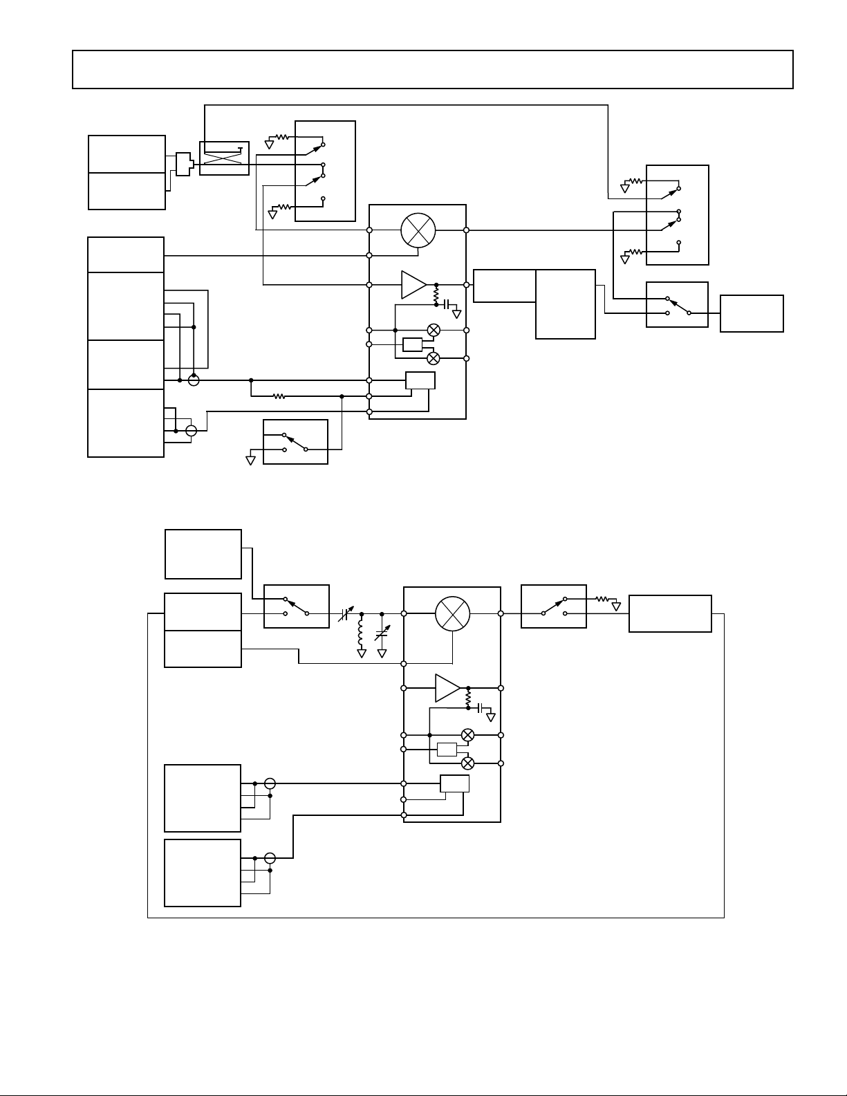
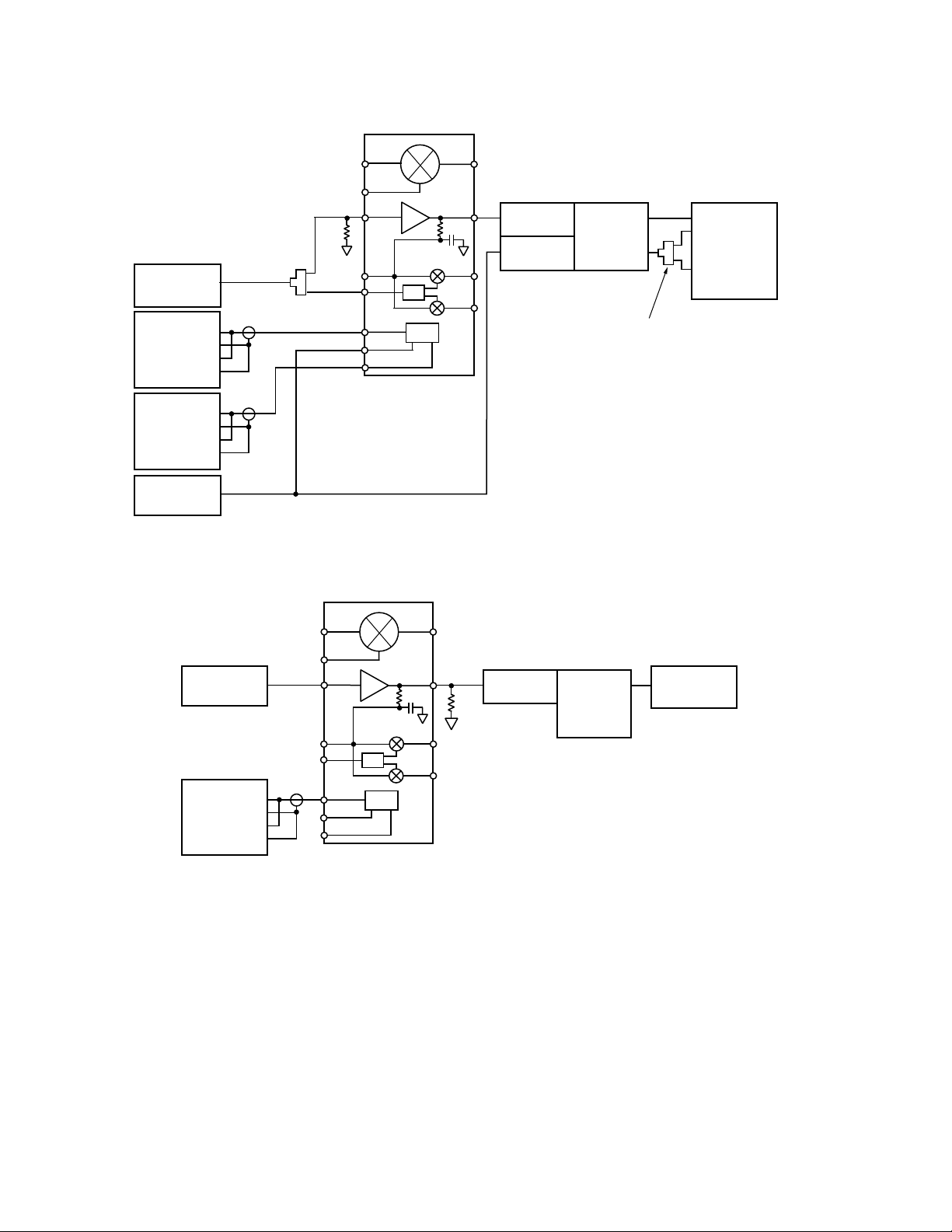
Figure 1 shows the main sections of the AD61009. It consists of
a variable-gain UHF mixer and linear four-stage IF strip, which
together provide a voltage controlled gain range of more than
90 dB; followed by dual demodulators, each comprising a multiplier followed by a two-pole, 2 MHz low-pass filter; and driven
by a phase-locked loop providing the inphase and quadrature
clocks. A biasing system with CMOS compatible power-down
completes the AD61009.
Mixer
The UHF mixer is an improved Gilbert cell design, and can
operate from low frequencies (it is internally dc-coupled) up to
an RF input of 500 MHz. The dynamic range at the input of the
mixer is determined, at the upper end, by the maximum input
signal level of ±56 mV between RFHI and RFLO up to which
the mixer remains linear, and, at the lower end, by the noise
level. It is customary to define the linearity of a mixer in terms
of the 1 dB gain-compression point and third-order intercept,
which for the AD61009 are –15 dBm and –8 dBm, respectively,
in a 50 Ω system.
The mixer’s RF input port is differential, that is, pin RFLO is
functionally identical to RFHI, and these nodes are internally
biased; we will generally assume that RFLO is decoupled to ac
ground. The RF port can be modeled as a parallel RC circuit as
shown in Figure 2.
AD61009
C1
C1, C2, L1: OPTIONAL MATCHING CIRCUIT
C3: COUPLES RFLO TO AC GROUND
C2
RFHI
R
C
IN
L1
C3
RFLO
IN
Figure 2. Mixer Port Modeled as a Parallel RC Network; an
Optional Matching Network Is also Shown
The local oscillator (LO) input is internally biased at VP/2 via a
nominal 1000 Ω resistor internally connected from pin LOIP to
VMID. The LO interface includes a preamplifier which minimizes
the drive requirements, thus simplifying the oscillator design
and reducing LO leakage from the RF port. Internally, this
single-sided input is actually differential; the noninverting input
is referenced to pin VMID. The LO requires a single-sided drive
of ± 50 mV, or –16 dBm in a 50 Ω system.
RFHI
RFLO
VPS1
VPS2
PRUP
LOIP
MIDPOINT
BIAS
GENERATOR
BIAS
GENERATOR
MXOP
VMID
COM1 COM2
VMID
PTAT
VOLTAGE
BPF
IFHI
IFLO
Figure 1. Functional Block Diagram
–14–
IFOP
BPF OR
LPF
DMIP
AD61009
VQFO
IOUT
FDIN
FLTR
QOUT
GAIN
GREF
REV. 0
Page 15

AD61009
The mixer’s output passes through both a low-pass filter and a
buffer, which provides an internal differential to single-ended
signal conversion with a bandwidth of approximately 45 MHz.
Its output at pin MXOP is in the form of a single-ended current.
This approach eliminates the 6 dB voltage loss of the usual series
termination by replacing it with shunt terminations at the both
the input and the output of the filter. The nominal conversion
gain is specified for operation into a total IF bandpass filter
(BPF) load of 165 Ω, that is, a 330 Ω filter, doubly-terminated
as shown in Figure 33. Note that these loads are connected to
bias point VMID, which is always at the midpoint of the supply
(that is, V
P
/2).
The conversion gain is measured between the mixer input and
the input of this filter, and varies between 1.5 dB and 26.5 dB
for a 165 Ω load impedance. Using filters of higher impedance,
the conversion gain can always be maintained at its specified
value or made even higher; for filters of lower impedance, of say
ZO, the conversion gain will be lowered by 10 log10(165/ZO).
Thus, the use of a 50 Ω filter will result in a conversion gain that
is 5.2 dB lower. Figure 3 shows filter matching networks and
Table I lists resistor values.
MXOP
VMID
R2
8
9
BPF
R1
100nF
1nF
R3
100nF
10
IFHI
IFLO
11
The maximum permissible signal level at MXOP is determined
by both voltage and current limitations. Using a 3 V supply and
VMID at 1.5 V, the maximum swing is about ±1.3 V. To attain
a voltage swing of ±1 V in the standard IF filter load of 165 Ω
load requires a peak drive current of about ±6 mA, which is well
within the linear capability of the mixer. However, these upper
limits for voltage and current should not be confused with issues
related to the mixer gain, already discussed. In an operational
system, the AGC voltage will determine the mixer gain, and
hence the signal level at the IF input pin IFHI; it will always be
less than ±56 mV (–15 dBm into 50 Ω), which is the limit of the
IF amplifier’s linear range.
IF Amplifier
Most of the gain in the AD61009 arises in the IF amplifier strip,
which comprises four stages. The first three are fully differential
and each has a gain span of 25 dB for the nominal AGC voltage
range. Thus, in conjunction with the mixer’s variable gain, the
total gain exceeds 90 dB. The final IF stage has a fixed gain of
20 dB, and it also provides differential to single-ended conversion.
The IF input is differential, at IFHI (noninverting relative to the
output IFOP) and IFLO (inverting). Figure 4 shows a simplified
schematic of the IF interface. The offset voltage of this stage
would cause a large dc output error at high gain, so it is nulled by
a low-pass feedback path from the IF output, also shown in
TPC 25. Unlike the mixer output, the signal at IFOP is a lowimpedance single-sided voltage, centered at V
/2 by the dc
P
feedback loop. It may be loaded by a resistance as low as 50 Ω,
which will normally be connected to VMID.
Figure 3. Suggested IF Filter Matching Network. The
Values of R1 and R2 Are Selected to Keep the Impedance
at Pin MXOP at 165
Ω
Table I. AD61009 Filter Termination Resistor Values for
Common IFs
Filter Filter Termination Resistor
IF Impedance Values1 for 24 dB of Mixer Gain
R1 R2 R3
450 kHz 1500 Ω 174 Ω 1330 Ω 1500 Ω
455 kHz 1500 Ω 174 Ω 1330 Ω 1500 Ω
6.5 MHz 1000 Ω 215 Ω 787 Ω 1000 Ω
10.7 MHz 330 Ω 330 Ω 0 Ω 330 Ω
NOTE
1
Resistor values were calculated such that R1 + R2 = Z
R1储 (R2 + Z
FILTER
) = 165 Ω.
FILTER
and
AD61009
LOOP
10k⍀
10k⍀
VMID
IFOP
IFHI
IFLO
OFFSET FEEDBACK
Figure 4. Simplified Schematic of the IF Interface
The IF’s small-signal bandwidth is approximately 45 MHz from
IFHI and IFLO through IFOP. The peak output at IFOP is
± 560 mV at V
= 3 V and ± 400 mV at the minimum VP of
P
2.7 V. This allows some headroom at the demodulator inputs
(pin DMIP), which accept a maximum input of ±150 mV for
IFs > 3 MHz and ±75 mV for IFs ≤ 3 MHz (at IFs ≤ 3 MHz,
the drive to the demodulators must be reduced to avoid saturating the output amplifiers with higher order mixing products that
are no longer removed by the onboard low-pass filters).
REV. 0
–15–
Page 16

AD61009
Since there is no band-limiting in the IF strip, the outputreferred noise can be quite high; in a typical application and
at a gain of 75 dB it is about 100 mV rms, making post-IF filtering
desirable. IFOP may be also used as an IF output for driving
an A/D converter, external demodulator, or external AGC
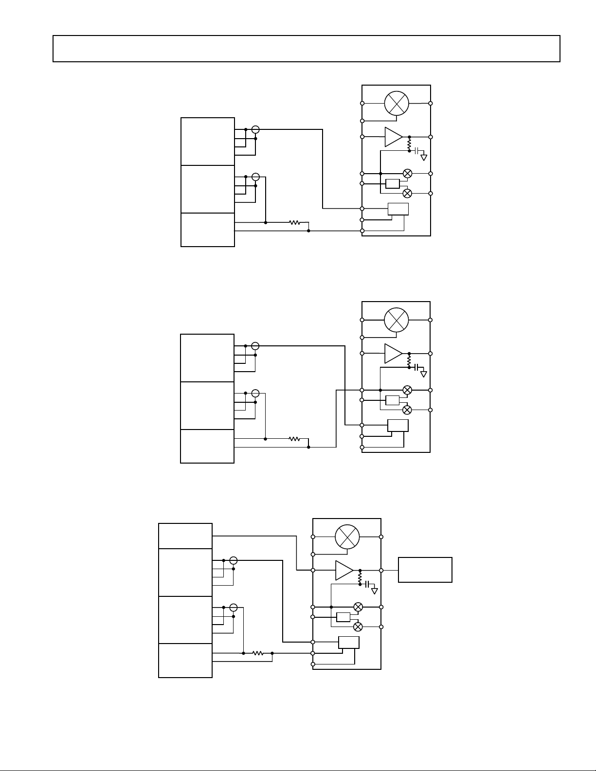
detector. Figure 5 shows methods of matching the optional
second IF filter.
BPF
VPOS
2R
T
2R
T
AD61009
IFOP
DMIP
R
T
a. Biasing DMIP from Power Supply (Assumes BPF AC
Coupled Internally)
AD61009
IFOP
DMIP
VMID
R
T
BPF
R
T
C
BYPASS
b. Biasing DMIP from VMID (Assumes BPF AC Coupled
Internally)
Figure 5. Input and Output Matching of the Optional
Second IF Filter
Gain Scaling and RSSI
The AD61009’s overall gain, expressed in decibels, is linearin-dB with respect to the AGC voltage V
gain of all sections is maximum when V
progressively up to V
– 0.8 V). The gain of all stages changes in parallel. The
limit V
P
= 2.2 V (for VP = 3 V; in general, up to a
G
at pin GAIN. The
G
is zero, and reduces
G
AD61009 features temperature-compensation of the gain scaling. The gain control scaling is proportional to the reference
voltage applied to the pin GREF. When this pin is tied to the
midpoint of the supply (VMID), the scale is nominally 20 mV/
dB (50 dB/V) for V
= 3 V. Under these conditions, the lower
P
80 dB of gain range (mixer plus IF) corresponds to a control
voltage of 0.4 V ≤ V
≤ 2.0 V. The final centering of this 1.6 V
G
range depends on the insertion losses of the IF filters used. More
generally, the gain scaling using these connections is V
/150
P
(volts per dB), so becomes 33.3 mV/dB (30 dB/V) using a 5 V
supply, with a proportional change in the AGC range, to 0.33 V ≤
≤ 3 V, Table II lists gain control voltages and scale factors
V
G
for power supply voltages from 3 V to 5.5 V.
Alternatively, pin GREF can be tied to an external voltage
reference, V
, provided, for example, by an AD1582 (2.5 V)
R
or AD1580 (1.21 V) voltage reference, to provide supplyindependent gain scaling of V
/75 (volts per dB). Since it uses
R
the same reference voltage, the numerical input to this DAC
provides an accurate RSSI value in digital form, no longer
requiring the reference voltage to have high absolute accuracy.
I/Q Demodulators
Both demodulators (I and Q) receive their inputs at pin DMIP.
Internally, this single-sided input is actually differential; the
noninverting input is referenced to pin VMID. Each demodulator comprises a full-wave synchronous detector followed by a
2 MHz, two-pole low-pass filter, producing single-sided outputs
at pins IOUT and QOT. Using the I and Q demodulators for
IFs above 12 MHz is precluded by the 1 MHz to 12 MHz
response of the PLL used in the demodulator section. Pin DMIP
requires an external bias source at V
/2; Figure 6 shows sug-
P
gested methods.
Outputs IOUT and QOUT are centered at V
/2 and can swing
P
up to ±1.23 V even at the low supply voltage of 2.85 V. The
conversion gain of the I and Q demodulators is 18 dB (X8),
requiring a maximum input amplitude at DMIP of ±150 mV
for IFs > 3 MHz.
Table II. AD61009 Gain and Manual Gain Control Voltage vs. Power Supply Voltage
Power Supply GREF Gain Control
Voltage (= VMID) Scale Factor Scale Factor Voltage Input Range
(V) (V) (dB/V) (mV/dB) (V)
3.0 1.5 50.00 20.00 0.400–2.000
3.5 1.75 42.86 23.33 0.467–2.333
4.0 2.0 37.50 26.67 0.533–2.667
4.5 2.25 33.33 30.00 0.600–3.000
5.0 2.5 30.00 33.33 0.667–3.333
5.5 2.75 27.27 36.67 0.733–3.667
NOTE
Maximum gain occurs for gain control voltage = 0 V.
–16–
REV. 0
Page 17

AD61009
BPF
VPOS
2R
T
2R
T
AD61009
IFOP
DMIP
R
T
a. Biasing DMIP from Power Supply (Assumes BPF
AC-Coupled Internally)
AD61009
IFOP
DMIP
VMID
R
T
BPF
R
T
C
BYPASS
b. Biasing DMIP from VMID (Assumes BPF
AC-Coupled Internally)
Figure 6. Suggested Methods for Biasing Pin DMIP
/2
at V
P
For IFs < 3 MHz, the on-chip low-pass filters (2 MHz cutoff)
do not attenuate the IF or feedthrough products; thus, the
maximum input voltage at DMIP must be limited to ±75 mV
to allow sufficient headroom at the I and Q outputs for not only
the desired baseband signal but also the unattenuated higherorder demodulation products. These products can be removed
by an external low-pass filter.
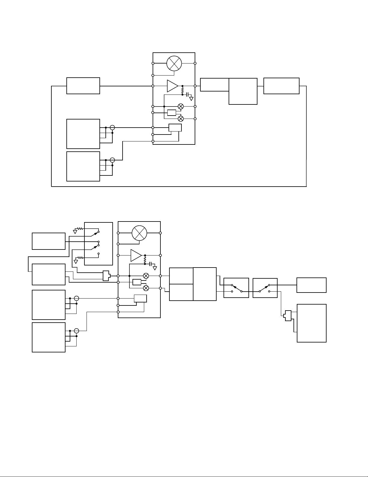
Phase-Locked Loop
The demodulators are driven by quadrature signals that are
provided by a variable frequency quadrature oscillator (VFQO),
phase locked to a reference signal applied to pin FDIN. When
this signal is at the IF, inphase and quadrature baseband outputs
are generated at IOUT and QOUT, respectively. The quadrature accuracy of this VFQO is typically –1.2° at 10.7 MHz. The
PLL uses a sequential-phase detector that comprises low power
emitter-coupled logic and a charge pump (Figure 7).
The reference signal may be provided from an external source,
in the form of a high-level clock, typically a low level signal
(± 400 mV) since there is an input amplifier between FDIN and
the loop’s phase detector. For example, the IF output itself can
be used by connecting DMIP to FDIN, which will then provide
automatic carrier recover for synchronous AM detection and
take advantage of any post-IF filtering. Pin FDIN must be
biased at V
/2; Figure 9 shows suggested methods.
P
The VFQO operates from 1 MHz to 12 MHz and is controlled by
the voltage between VPOS and FLTR. In normal operation, a
series RC network, forming the PLL loop filter, is connected
from FLTR to ground. The use of an integral sample-hold
system ensures that the frequency-control voltage on pin FLTR
remains held during power-down, so reacquisition of the carrier
typically occurs in 16.5 µs.
In practice, the probability of a phase mismatch at power-up is
high, so the worst-case linear settling period to full lock needs to
be considered in making filter choices. This is typically 16.5 µs at
an IF of 10.7 MHz for a ±100 mV signal at DMIP and FDIN.
Bias System
The AD61009 operates from a single supply, VP, usually of 3 V,
at a typical supply current of 8.5 mA at midgain and T = 27°C,
corresponding to a power consumption of 25 mW. Any voltage
from 2.85 V to 5.5 V may be used.
The bias system includes a fast-acting active-high CMOScompatible power-up switch, allowing the part to idle at 550 µA
when disabled. Biasing is proportional-to-absolute-temperature
(PTAT) to ensure stable gain with temperature.
An independent regulator generates a voltage at the midpoint
of the supply (V
/2) which appears at the VMID pin, at a low
P
impedance. This voltage does not shut down, ensuring that the
major signal interfaces (e.g., mixer-to-IF and IF-to-demodulators)
remain biased at all times, thus minimizing transient disturbances
at power-up and allowing the use of substantial decoupling
capacitors on this node. The quiescent consumption of this
regulator is included in the idling current.
EXTERNAL
FREQUENCY
REFERENCE
VPOS
50k⍀
50k⍀
AD61009
FDIN
IU~
40A
V
F
SEQUENTIAL
PHASE
DETECTOR
R
REFERENCE CARRIER
(FDIN AFTER LIMITING)
F
U
D
~
I
D
40A
VARIABLE-
FREQUENCY
QUADRATURE
OSCILLATOR
C
R
I-CLOCK
90ⴗ
Q-CLOCK
(ECL OUTPUTS)
Figure 7. Simplified Schematic of the PLL and
Quadrature VCO
REV. 0
a. Biasing FDIN from Supply when Using
External Frequency Reference
AD61009
EXTERNAL
FREQUENCY
REFERENCE
50k⍀
C
BYPASS
FDIN
VMID
b. Biasing FDIN from VMID when Using
External Frequency Reference
Figure 8. Suggested Methods for Biasing Pin FDIN
/2
at V
P
–17–
Page 18

AD61009
USING THE AD61009
In this section, we will focus on a few areas of special importance and include a few general application tips. As is true of
any wideband high gain component, great care is needed in PC
board layout. The location of the particular grounding points
must be considered with due regard to possibility of unwanted
signal coupling, particularly from IFOP to RFHI or IFHI or both.
The high sensitivity of the AD61009 leads to the possibility that
unwanted local EM signals may have an effect on the performance.
During system development, carefully-shielded test assemblies
should be used. The best solution is to use a fully-enclosed
box enclosing all components, with the minimum number of
needed signal connectors (RF, LO, I and Q outputs) in miniature coax form.
The I and Q output leads can include small series resistors
(about 100 Ω) inside the shielded box without significant loss
of performance, provided the external loading during testing
is light (that is, a resistive load of more than 20 kΩ and capacitances of a few picofarads). These help to keep unwanted RF
emanations out of the interior.
The power supply should be connected via a through-hole
capacitor with a ferrite bead on both inside and outside leads.
Close to the IC pins, two capacitors of different value should be
used to decouple the main supply (V
) and the midpoint supply
P
pin, VMID. Guidance on these matters is also generally included
in applications schematics.
Gain Distribution
As in all receivers, the most critical decisions in effectively using
the AD61009 relate to the partitioning of gain between the
various subsections (Mixer, IF Amplifier, Demodulators) and
the placement of filters, so as to achieve the highest overall signalto-noise ratio and lowest intermodulation distortion.
Figure 9 shows the main RF/IF signal path at maximum and
minimum signal levels.
As noted earlier, the gain in dB is reduced linearly with the
voltage V
and IF strip gains vary with V
on the GAIN pin. Figure 10 shows how the mixer
G
when GREF is connected to VMID
G
(1.5 V) and a supply voltage of 3 V is used. Figure 11 shows
how these vary when GREF is connected to a 1.23 V reference.
90dB
80dB
70dB
60dB
50dB
40dB
30dB
20dB
10dB
0dB
01V2V
(67.5dB)
IF GAIN
(21.5dB)
0.4V 1.8V
NORMAL OPERATING RANGE
MIXER GAIN
V
(7.5dB)
(1.5dB)
2.2V
g
Figure 10. Gain Distribution for GREF = 1.5 V
90dB
80dB
70dB
60dB
50dB
40dB
30dB
20dB
10dB
0dB
01V2V
(67.5dB)
IF GAIN
(21.5dB)
MIXER GAIN
0.328V 1.64V
NORMAL OPERATING RANGE
(7.5dB)
(1.5dB)
V
g
Figure 11. Gain Distribution for GREF = 1.23 V
ⴞ54mV
MAX INPUT
RFHI
MAX OUTPUT
LOIP
CONSTANT
–16dBm
(ⴞ50mV)
ⴞ1.3V
MXOP IFHI
ⴞ54mV
MAX INPUT
IF BPF IF BPF
330⍀330⍀
(TYPICAL
IMPEDANCE)
ⴞ560mV
MAX OUTPUT
(VMID)
(LOCATION OF OPTIONAL
SECOND IF FILTER)
ⴞ154mV
MAX INPUT
DMIPIFOP
Figure 9. Signal Levels for Minimum and Maximum Gain
–18–
I
Q
ⴞ1.23V
MAX OUTPUT
IOUT
QOUT
REV. 0
Page 19

AD61009
Using the AD61009 with a Fast PRUP Control Signal
If the AD61009 is used in a system in which the PRUP signal
(Pin 3) is applied with a rise time less than 35 µs, anomalous
behavior occasionally occurs. The problem is intermittent, so it
will not occur every time the part is powered up under these
conditions. It does not occur for any other normal operating conditions when the PRUP signal has a rise time slower than 35 µs.
Symptoms of operation with too fast a PRUP signal include low
gain, oscillations at the I or Q outputs of the device or no valid
data occurring at the output of the AD61009. The problem
causes no permanent damage to the AD61009, so it will often
operate normally when reset.
Fortunately, there is a very simple solution to the fast PRUP
problem. If the PRUP signal (Pin 3) is slowed down so that
the rise time of the signal edge is greater than 35 µs, the anoma-
lous behavior will not occur. This can be realized by a simple
RC circuit connected to the PRUP pin, where R = 4.7 kΩ and
C = 1.5 nF. This circuit is shown in Figure 12.
FROM PRUP
CONTROL SIGNAL
4.7k⍀
1.5nF
AD61009
PRUP
All designs incorporating the AD61009 should include
this circuitry.
Note that connecting the PRUP pin to the supply voltage will
not eliminate the problem since the supply voltage may have a
rise time faster than 35 µs. With this configuration, the 4.7 kΩ
series R and 1.5 nF shunt C should be placed between the
supply and the PRUP pin as shown in Figure 12.
AD61009 EVALUATION BOARD
The AD61009 evaluation board (Figures 13 and 14) consists of
an AD61009, ground plane, I/O connectors, and a 10.7 MHz
bandpass filter. The RF and LO ports are terminated in 50 Ω
to provide a broadband match to external signal generators to
allow a choice of RF and LO input frequencies. The IF filter is
at 10.7 MHz and has 330 Ω input and output terminations; the
board is laid out to allow the user to substitute other filters for
other IFs.
The board provides SMA connectors for the RF and LO port
inputs, the demodulated I and Q outputs, the manual gain control (MGC) input, the PLL input, and the power-up input. In
addition, the IF output is also available at an SMA connector;
this may be connected to the PLL input for carrier recovery to
realize synchronous AM and FM detection via the I and Q
demodulators, respectively. Table III lists the AD61009 Evaluation Board’s I/O Connectors and their functions.
Figure 12. Proper Configuration of AD61009 PRUP Signal
REV. 0
–19–
Page 20

AD61009
VPOS
GND
FDIN
PRUP
LO
RF
C13 0
C14 0
C15
0.1F
R8
51.1⍀
C11
10nF
R7
51.1⍀
R6
51.1⍀
C10
1nF
FDIN
JUMPER
0.1F
R12
4.7k⍀
C9
1nF
R5
332⍀
R3
332⍀
C12
C17
1.5nF
R10
4.99k⍀
AD607 EVALUATION BOARD
SHORT
R14
C17
51.1⍀
10nF
1nF
C16
JUMPER
R4
OPEN
C7
1nF
(AS RECEIVED)
C18
R11
OPEN
FDIN
COM1
PRUP
LOIP
RFLO
RFHI
GREF
MXOP
VMID
IFHI
R12
OPEN
50k⍀
AD61009
R15
VPS1
FLTR
IOUT
QOUT
VPS2
DMIP
IFOP
COM2
GAIN
IFLO
R13
50k⍀
VPOS
FDIN
C1
0.1F
R1
1k⍀
C20.1F
R2
316⍀
C6
0.1F
C8
0.1F
C3 10nF
47pF
C5
1nF
I
C4
Q
IF
GAIN
FDIN
VMID
MOD FOR LARGE MAGNITUDE
AC-COUPLED INPUT
VMID
OPEN
R16
OPEN
R19
RSOURCE
C19
ANYTHING
C20
SHORT
MOD FOR DC-COUPLED INPUT
Figure 13. Evaluation Board
R17
R18
OPEN
VPOS
FDIN
–20–
REV. 0
Page 21

FDIN
AD61009
PRUP
C13 C10
C14
LOIP
RFHI
J10
R8
R12
C17
R7
R6
ANALOG
DEVICES
AD61009
EVALUATION BOARD REV B
C11
C16
C9
J9
a. Topside
C15
FILT
C12
R1
C2
C3
C3'
C4
C6
C8
IFOP
R10
R11
C1
U1
R4
R5
R3
C7
R2
R9
C5
b. Bottom Side
Figure 14. Evaluation Board Layout
IOUT
QOUT
GAIN
REV. 0
–21–
Page 22

AD61009
Table III. AD61009 Evaluation Board Input and Output Connections
Reference Connector Approximate
Designation Type Description Coupling Signal Level Comments
J1 SMA Frequency DC ± 400 mV This pin needs to be biased at VMID
Detector Input and ac coupled when driven by an
external signal generator.
J2 SMA Power Up DC CMOS Logic Tied to Positive Supply by Jumper J10.
Level Input
J3 SMA LO Input AC –16 dBm Input is terminated in 50 Ω.
(± 50 mV)
J4 SMA RF Input AC –15 dBm max Input is terminated in 50 Ω.
(± 54 mV)
J5 SMA MGC Input DC 0.4 V to 2.0 V Jumper is set for Manual Gain Control
(3 V Supply) Input; See Table I for Control Voltage
(GREF = VMID) Values.
J6 SMA IF Output AC NA This signal level depends on the
AD61009’s gain setting.
J7 SMA Q Output AC NA This signal level depends on the
AD61009’s gain setting.
J8 SMA I Output AC NA This signal level depends on the
AD61009’s gain setting.
J9 Jumper Ties GREF NA NA Sets gain-control Scale Factor (SF);
to VMID SF = 75/VMID in dB/V, where
VMID = VPOS/2.
J10 Jumper Ties Power-Up NA NA Remove to test Power-Up/-Down.
to Positive
Supply
T1 Terminal Pin Power Supply DC DC 2.85 V to 5.5 V
Positive Input Draws 8.5 mA at midgain connection.
(VPS1, VPS2)
T2 Terminal Pin Power Supply DC 0 V
Return (GND)
–22–
REV. 0
Page 23

AD61009
In operation (Figure 15), the AD61009 evaluation board draws
about 8.5 mA at midgain (59 dB). Use high impedance probes
to monitor signals from the demodulated I and Q outputs and
the IF output. The MGC voltage should be set such that the
signal level at DMIP does not exceed ±150 mV; signal levels
HP 6632A
PROGRAMMABLE
POWER SUPPLY
2.7V–6V
FLUKE 6082A
SYNTHESIZED
SIGNAL GENERATOR
240MHz
HP 8656A
SYNTHESIZED
SIGNAL GENERATOR
240.02MHz
IEEE CONTROLLER
MCL
ZFSC–2–1
COMBINER
HP 9920
HP9121
DISK DRIVE
RF
LO
HP 8656A
SYNTHESIZED
SIGNAL GENERATOR
229.3MHz
above this will overload the I and Q demodulators. The insertion loss between IFOP and DMIP is typically 3 dB if a simple
low-pass filter (R8 and C2) is used and higher if a reverseterminated bandpass filter is used.
HP 3326
SYNTHESIZED
SIGNAL GENERATOR
10.710MHz
VPOS FDIN
AD607
EVALUATION
BOARD
I OUTPUT
Q OUTPUT
MGC
DATA PRECISION
DVC8200
PROGRAMMABLE
VOLTAGE SOURCE
TEKTRONIX
11402A
OSCILLOSCOPE
WITH 11A32
PLUGIN
Figure 15. Evaluation Board Test Setup
IEEE–488 BUS
REV. 0
–23–
Page 24

AD61009
OUTLINE DIMENSIONS
Dimensions shown in inches and (mm).
20-Lead Plastic SSOP (RS-20)
0.295 (7.50)
0.271 (6.90)
20 11
0.311 (7.9)
0.301 (7.64)
0.078 (1.98)
0.068 (1.73)
0.008 (0.203)
0.002 (0.050)
PIN 1
0.0256
(0.65)
BSC
101
0.07 (1.78)
0.066 (1.67)
SEATING
PLANE
0.212 (5.38)
0.205 (5.21)
0.009 (0.229)
0.005 (0.127)
8°
0°
C02347–0–1/01 (rev. 0)
0.037 (0.94)
0.022 (0.559)
–24–
PRINTED IN U.S.A.
REV. 0
 Loading...