

Page 1
Low Power Mixer/AGC/RSSI
14
13
12
11
17
16
15
20
19
18
10
9
8
1
2
3
4
7
6
5
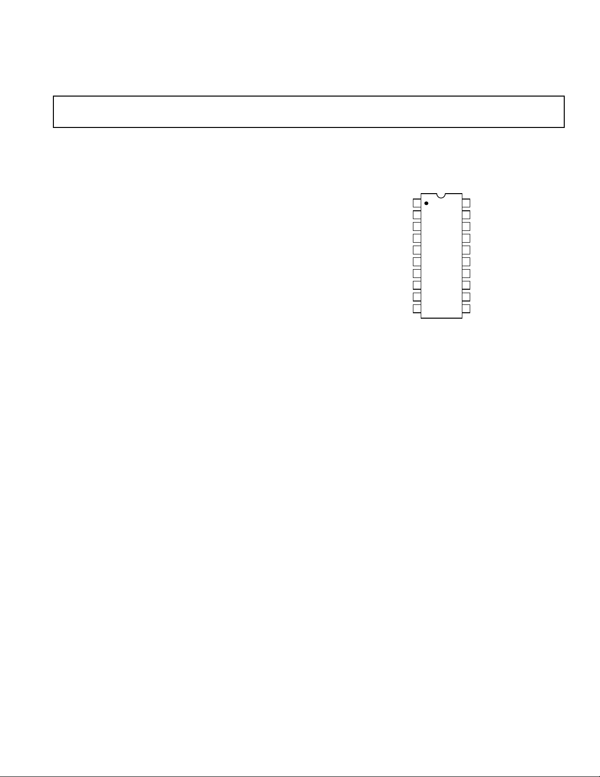
TOP VIEW
(Not to Scale)
AD607
FDIN
QOUT
IOUT
FLTR
VPS1
COM1
PRUP
LOIP
IFOP
DMIP
VPS2
RFLO
RFHI
GREF
MXOP
VMID
IFHI
IFLO
GAIN/RS
COM2
a
FEATURES
Complete Receiver on a Chip: Monoceiver™ Mixer
–15 dBm 1 dB Compression Point
–8 dBm Input Third Order Intercept
500 MHz RF and LO Bandwidths
Linear IF Amplifier
Linear-in-dB Gain Control
MGC or AGC with RSSI Output
Quadrature Demodulator
On-Board Phase-Locked Quadrature Oscillator
Demodulates IFs from 400 kHz to 12 MHz
Can Also Demodulate AM, CW, SSB
Low Power
25 mW at 3 V
CMOS Compatible Power-Down
Interfaces to AD7013 and AD7015 Baseband Converters
APPLICATIONS
GSM, CDMA, TDMA, and TETRA Receivers
Satellite Terminals
Battery-Powered Communications Receivers
3 V Receiver IF Subsystem
AD607
PIN CONFIGURATION
20-Lead SSOP
(RS Suffix)
GENERAL DESCRIPTION
The AD607 is a 3 V low power receiver IF subsystem for operation at input frequencies as high as 500 MHz and IFs from
400 kHz to 12 MHz. It consists of a mixer, IF amplifiers, I and
Q demodulators, a phase-locked quadrature oscillator, AGC
detector, and a biasing system with external power-down.
The AD607’s low noise, high intercept mixer is a doublybalanced Gilbert cell type. It has a nominal –15 dBm input
referred 1 dB compression point and a –8 dBm input referred
third-order intercept. The mixer section of the AD607 also
includes a local oscillator (LO) preamplifier, which lowers the
required LO drive to –16 dBm.
The gain control input can serve as either a manual gain control
(MGC) input or an automatic gain control (AGC) voltagebased RSSI output. In MGC operation, the AD607 accepts an
external gain-control voltage input from an external AGC detector or a DAC. In AGC operation, an onboard detector and an
external averaging capacitor form an AGC loop that holds the
IF output level at ±300 mV. The voltage across this capacitor
then provides an RSSI output.
REV. 0
Information furnished by Analog Devices is believed to be accurate and
reliable. However, no responsibility is assumed by Analog Devices for its
use, nor for any infringements of patents or other rights of third parties
which may result from its use. No license is granted by implication or
otherwise under any patent or patent rights of Analog Devices.
The I and Q demodulators provide inphase and quadrature
baseband outputs to interface with Analog Devices’ AD7013
(IS54, TETRA, MSAT) and AD7015 (GSM) baseband converters. A quadrature VCO phase-locked to the IF drives the I
and Q demodulators. The I and Q demodulators can also demodulate AM; when the AD607’s quadrature VCO is phase
locked to the received signal, the in-phase demodulator becomes
a synchronous product detector for AM. The VCO can also be
phase-locked to an external beat-frequency oscillator (BFO),
and the demodulator serves as a product detector for CW or
SSB reception. Finally, the AD607 can be used to demodulate
BPSK using an external Costas Loop for carrier recovery.
© Analog Devices, Inc., 1995
One Technology Way, P.O. Box 9106, Norwood. MA 02062-9106, U.S.A.
Tel: 617/329-4700 Fax: 617/326-8703
Page 2

AD607–SPECIFICATIONS
(@ TA = + 25°C, Supply = 3.0 V, IF = 10.7 MHz, unless otherwise noted)
Model AD607ARS
Conditions Min Typ Max Units
DYNAMIC PERFORMANCE
MIXER
Maximum RF and LO Frequency Range For Conversion Gain > 20 dB 500 MHz
Maximum Mixer Input Voltage For Linear Operation; Between RFHI and RFLO ±54 mV
Input 1 dB Compression Point RF Input Terminated in 50 Ω –15 dBm
Input Third-Order Intercept RF Input Terminated in 50 Ω –5 dBm
Noise Figure Matched Input, Max Gain, f = 83 MHz, IF = 10.7 MHz 14 dB
Matched Input, Max Gain, f = 144 MHz, IF = 10.7 MHz 12 dB
Maximum Output Voltage at MXOP Z
Mixer Output Bandwidth at MXOP –3 dB, Z
= 165 Ω, at Input Compression ±1.3 V
IF
= 165 Ω 45 MHz
IF
LO Drive Level Mixer LO Input Terminated in 50 Ω –16 dBm
LO Input Impedance LOIP to VMID 1 kΩ
Isolation, RF to IF RF = 240 MHz, IF = 10.7 MHz, LO = 229.3 MHz 30 dB
Isolation, LO to IF RF = 240 MHz, IF = 10.7 MHz, LO = 229.3 MHz 20 dB
Isolation, LO to RF RF = 240 MHz, IF = 10.7 MHz, LO = 229.3 MHz 40 dB
Isolation, IF to RF RF = 240 MHz, IF = 10.7 MHz, LO = 229.3 MHz 70 dB
IF AMPLIFIERS
Noise Figure Max Gain, f = 10.7 MHz 17 dB
Input 1 dB Compression Point IF = 10.7 MHz –15 dBm
Output Third-Order Intercept IF = 10.7 MHz +18 dBm
Maximum IF Output Voltage at IFOP Z
= 600 Ω±560 mV
IF
Output Resistance at IFOP From IFOP to VMID 15 Ω
Bandwidth –3 dB at IFOP, Max Gain 45 MHz
GAIN CONTROL (See Figures 43 and 44)
Gain Control Range Mixer + IF Section, GREF to 1.5 V 90 dB
Gain Scaling GREF to 1.5 V 20 mV/dB
GREF to General Reference Voltage V
R
75/V
R
dB/V
Gain Scaling Accuracy GREF to 1.5 V, 80 dB Span ±1dB
Bias Current at GAIN/RSSI 5 µA
Bias Current at GREF 1 µA
Input Resistance at GAIN, GREF 1MΩ
I AND Q DEMODULATORS
Required DC Bias at DMIP VPOS/2 V dc
Input Resistance at DMIP From DMIP to VMID 50 kΩ
Input Bias Current at DMIP 2 µA
Maximum Input Voltage IF > 3 MHz ±150 mV
IF ≤ 3 MHz ±75 mV
Amplitude Balance IF = 10.7 MHz, Outputs at 600 mV p-p, F = 100 kHz ±0.2 dB
Quadrature Error IF = 10.7 MHz, Outputs at 600 mV p-p, F = 100 kHz –1.2 Degrees
Phase Noise in Degrees IF = 10.7 MHz, F = 10 kHz –100 dBc/Hz
Demodulation Gain Sine Wave Input, Baseband Output 18 dB
Maximum Output Voltage R
Output Offset Voltage Measured from I
≥ 20 kΩ±1.23 V
L
OUT
, Q
to VMID 10 mV
OUT
Output Bandwidth Sine Wave Input, Baseband Output 1.5 MHz
PLL
Required DC Bias at FDIN VPOS/2 V dc
Input Resistance at FDIN From FDIN to VMID 50 kΩ
Input Bias Current at FDIN 200 nA
Frequency Range 0.4 to 12 MHz
Required Input Drive Level Sine Wave Input at Pin 1 400 mV
Acquisition Time to ±3° IF = 10.7 MHz 16.5 µs
POWER-DOWN INTERFACE
Logical Threshold For Power Up on Logical High 2 V dc
Input Current for Logical High 75 µA
Turn-On Response Time To PLL Locked 16.5 µs
Standby Current 550 µA
POWER SUPPLY
Supply Range 2.7 5.5 V
Supply Current Midgain, IF = 10.7 MHz 8.5 mA
OPERATING TEMPERATURE
T
MIN
to T
MAX
Operation to 2.7 V Minimum Supply Voltage –25 +85 °C
Operation to 4.5 V Minimum Supply Voltage –40 +85 °C
Specifications subject to change without notice.
–2–
REV. 0
Page 3

AD607
WARNING!
ESD SENSITIVE DEVICE
ABSOLUTE MAXIMUM RATINGS
Supply Voltage VPS1, VPS2 to COM1, COM2 . . . . . . . +5.5 V
Internal Power Dissipation
2
. . . . . . . . . . . . . . . . . . . . 600 mW
1
2.7 V to 5.5 V Operating Temperature Range
. . . . . . . . . . . . . . . . . . . . . . . . . . . . . . . . . . . –25°C to +85°C
4.5 V to 5.5 V Operating Temperature Range
. . . . . . . . . . . . . . . . . . . . . . . . . . . . . . . . . . . – 40°C to +85°C
Storage Temperature Range . . . . . . . . . . . . –65°C to +150°C
Lead Temperature Range (Soldering 60 sec) . . . . . . . . +300°C
NOTES
1
Stresses above those listed under “Absolute Maximum Ratings” may cause
permanent damage to the device. This is a stress rating only and functional
operation of the device at these or any other conditions above those indicated in
the operational section of this specification is not implied. Exposure to absolute
maximum rating conditions for extended periods may affect device reliability.
2
Thermal Characteristics: 20-lead SSOP Package: θJA = 126°C/W.
Model Range Description Option
AD607ARS –25°C to +85°C 20-Pin Plastic RS-20
ORDERING GUIDE
Temperature Package Package
for 2.7 V to 5.5 V SSOP
Operation; –40°C
to +85°C for 4.5 V
to 5.5 V Operation
CAUTION
ESD (electrostatic discharge) sensitive device. Electrostatic charges as high as 4000 V readily
accumulate on the human body and test equipment and can discharge without detection.
Although the AD607 features proprietary ESD protection circuitry, permanent damage may
occur on devices subjected to high energy electrostatic discharges. Therefore, proper ESD
precautions are recommended to avoid performance degradation or loss of functionality.
REV. 0
–3–
Page 4
AD607
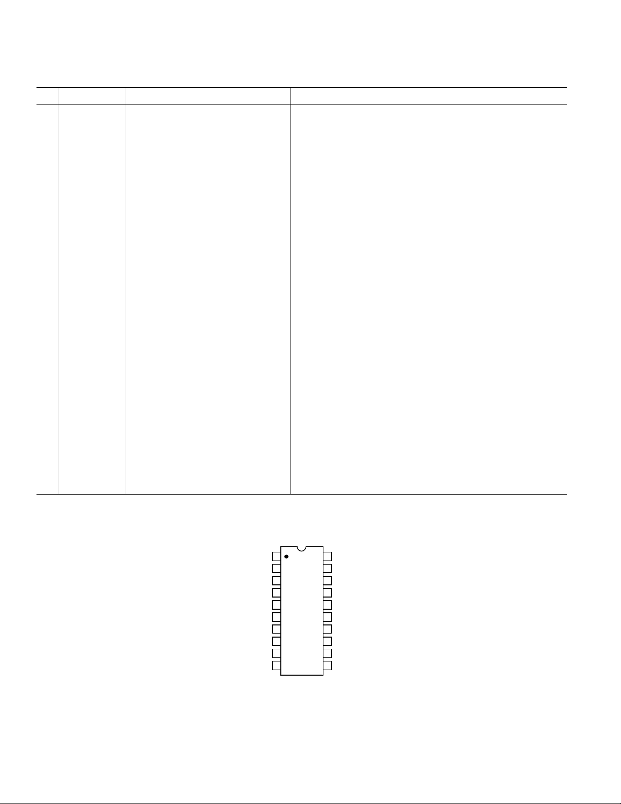
PIN DESCRIPTION
Pin Mnemonic Reads Function
1 FDIN Frequency Detector Input PLL input for I/Q demodulator quadrature oscillator, ± 400 mV
drive required from external oscillator. Must be biased at V
2 COM1 Common #1 Supply common for RF front end and main bias.
3 PRUP Power-Up Input 3 V/5 V CMOS compatible power-up control; logical high =
powered-up; max input level = VPS1 = VPS2.
4 LOIP Local Oscillator Input LO input, ac coupled ±54 mV LO input required (–16 dBm for
50 Ω input termination).
5 RFLO RF “Low” Input Usually connected to ac ground.
6 RFHI RF “High” Input AC coupled, ±56 mV, max RF input for linear operation.
7 GREF Gain Reference Input High impedance input, typically 1.5 V, sets gain scaling.
8 MXOP Mixer Output High impedance, single-sided current output, ± 1.3 V max voltage
output (±6 mA max current output).
9 VMID Midsupply Bias Voltage Output of the midsupply bias generator (VMID = VPOS/2).
10 IFHI IF “High” Input AC coupled IF input, ±56 mV max input for linear operation.
11 IFLO IF “Low” Voltage Reference node for IF input; auto-offset null.
12 GAIN/RSSI Gain Control Input/RSSI Output High impedance input, 0 V–2 V using 3 V supply, max gain at
V = 0. RSSI Output when using Internal AGC Detector; RSSI
voltage is across AGC Capacitor connected to this pin.
13 COM2 Common #2 Supply common for IF stages and demodulator.
14 IFOP IF Output Low impedance, single-sided voltage output, +5 dBm (± 560 mV)
max.
15 DMIP Demodulator Input Signal input to I and Q demodulators ±150 mV max input at IF
> 3 MHz for linear operation; ±75 mV max input at IF < 3 MHz
for linear operation. Must be biased at V
/2.
P
16 VPS2 VPOS Supply #2 Supply to high-level IF, PLL, and demodulators.
17 QOUT Quadrature Output Low impedance Q baseband output ±1.23 V full scale in 20 kΩ
min load; ac coupled.
18 IOUT In-Phase Output Low impedance I baseband output; ±1.23 V full scale in 20 kΩ
min load; ac coupled.
19 FLTR PLL Loop Filter Series RC PLL Loop filter, connected to ground.
20 VPS1 VPOS Supply #1 Supply to mixer, low level IF, PLL, and gain control.
/2.
P
PIN CONNECTION
20-Pin SSOP (RS-20)
VPS1
FDIN
COM1
PRUP
LOIP
RFLO
RFHI
GREF
MXOP
VMID
IFHI
1
2
3
4
5
AD607
TOP VIEW
6
(Not to Scale)
7
8
9
10
20
19
18
17
16
15
14
13
12
11
FLTR
IOUT
QOUT
VPS2
DMIP
IFOP
COM2
GAIN/RS
IFLO
–4–
REV. 0
Page 5
HP8656B
IEEE
SYNTHESIZER
HP8656B
IEEE
SYNTHESIZER
HP8656B
IEEE
SYNTHESIZER
HP6633A
IEEE
DCPS
HP34401A
CPIB
DMM
DP8200
IEEE
V
REF
RF_OUT
RF_OUT
RF_OUT
VPOS
VNEG
SPOS
SNEG
VPOS
VNEG
SPOS
SNEG
Typical Performance Characteristics–AD607
HP8764B
50Ω
50Ω
HI
LO
I
0
1
R5
1kΩ
HP8765B
S0
0
1
S0
0
S1
CHARACTERIZATION
RFHI
LOIP
IFHI
DMIP
FDIN
VPOS
PRUP
GAIN
BOARD
R
PLL
BIAS
MXOP
X
L
IFOP
IOUT
QOUT
X10
FET
P6205
PROBE
OUT
IN1 OUT1
IN2 OUT2
PROBE SUPPLY
TEK1105
1
V
C
S1V
HP8764B
50Ω
50Ω
0
1
S0
0
S1
1
V
HP8765B
0
1C
S0
S1V
RF_IN
HP8594E
SPEC
IEEE
AN
HP8720C
IEEE_488
NETWORK AN
HP346B
28V
NOISE SOURCE
HP8656B
IEEE
SYNTHESIZER
HP6633A
IEEE
DCPS
DP8200
IEEE
V
REF
PORT_1
PORT_2
NOISE
RF_OUT
VPOS
VNEG
SPOS
SNEG
VPOS
VNEG
SPOS
SNEG
Figure 1. Mixer/Amplifier Test Set
HP8765B
0
1C
S0
S1
V
CHARACTERIZATION
BOARD
RFHI
LOIP
IFHI
DMIP
FDIN
VPOS
PRUP
GAIN
X
R
L
PLL
BIAS
MXOP
IFOP
IOUT
QOUT
C
HP8765B
S1 V
50Ω
0
1
S0
HP8970A
RF_IN
NOISE FIGURE METER
28V_OUT
REV. 0
Figure 2. Mixer Noise Figure Test Set
–5–
Page 6
AD607
CHARACTERIZATION
BOARD
HP8656B
IEEE
IEEE
IEEE
IEEE
RF_OUT
SYNTHESIZER
HP3326A
OUTPUT_1
DCFM
OUTPUT_2
DUAL SYNTHESIZER
HP6633A
VPOS
VNEG
SPOS
SNEG
DCPS
DP8200
VPOS
VNEG
SPOS
SNEG
V
REF
HP346B
28V
NOISE SOURCE
HP6633A
IEEE
DCPS
DP8200
IEEE
V
50Ω
50Ω
REF
NOISE
VPOS
VNEG
SPOS
SNEG
VPOS
VNEG
SPOS
SNEG
HP8764B
1
RFHI
LOIP
IFHI
DMIP
FDIN
VPOS
PRUP
GAIN
MXOP
X
R
L
PLL
BIAS
IFOP
IOUT
QOUT
X10
FET
P6205
PROBE
OUT
IN1 OUT1
IN2 OUT2
PROBE SUPPLY
TEK1103
HP8970A
RF_IN
NOISE FIGURE METER
28V_OUT
Figure 3. IF Amp Noise Figure Test Set
CHARACTERIZATION
BOARD
0
1
0
RFHI
LOIP
S0
S1
IFHI
V
DMIP
FDIN
VPOS
PRUP
GAIN
MXOP
X
R
L
IFOP
OUT
IN1
OUT
IN2
PROBE SUPPLY
1103
OUT1
OUT2
HP8765B
0
1C
S0
S1
V
HP8765B
C
S1 V
0
1
S0
HP8694E
RF_IN IEEE
SPEC AN
HP54120
CH1
CH2
CH3
CH4
TRIG IEEE_488
DIGITAL
OSCILLOSCOPE
PLL
BIAS
IOUT
QOUT
P6205
X10
FET PROBE
P6205
X10
FET PROBE
Figure 4. PLL/Demodulator Test Set
–6–
REV. 0
Page 7
CHARACTERIZATION
DP8200
IEEE
VPOS
VNEG
SPOS
SNEG
V
REF
HP34401A
GPIB
HI
LO
I
DMM
HP6633A
IEEE
VPOS
VNEG
SPOS
SNEG
DCPS
R1
499kΩ
MXOP
RFHI
LOIP
L
R
X
IFOP
IFHI
PLL
IOUT
QOUT
DMIP
FDIN
BIAS
VPOS
PRUP
GAIN
CHARACTERIZATION
BOARD
BOARD
AD607
IEEE
IEEE
GPIB
HP6633A
DCPS
DP8200
V
REF
HP34401A
DMM
VPOS
VNEG
SPOS
SNEG
VPOS
VNEG
SPOS
SNEG
HI
LO
I
R1
499kΩ
Figure 5. GAIN Pin Bias Test Set
RFHI
LOIP
IFHI
DMIP
FDIN
VPOS
PRUP
GAIN
MXOP
R
X
L
IFOP
IOUT
PLL
QOUT
BIAS
REV. 0
Figure 6. Demodulator Bias Test Set
CHARACTERIZATION
BOARD
HP3325B
RF_OUT
IEEE
SYNTHESIZER
HP6633A
VPOS
VNEG
DCPS
DCPS
DMM
SPOS
SNEG
VPOS
VNEG
SPOS
SNEG
LO
R1
HI
I
Figure 7. Power-Up Threshold Test Set
10kΩ
IEEE
HP6633A
IEEE
HP34401A
GPIB
–7–
RFHI
LOIP
IFHI
DMIP
FDIN
VPOS
PRUP
GAIN
MXOP
R
X
L
HP8594E
RF_IN IEEE
SPEC AN
PLL
IFOP
IOUT
QOUT
BIAS
Page 8
AD607
CHARACTERIZATION
BOARD
FL6082A
RF_OUT
IEEE
MOD_OUT
HP6633A
VPOS
DCPS
DP8200
V
REF
HP8112
PULSE_OUT
SYNTHESIZER
IEEE
VNEG
SPOS
SNEG
VPOS
VNEG
SPOS
SNEG
HP8656B
HP6633A
IEEE
IEEE
IEEE
PULSE GENERATOR
DCPS
RFHI
LOIP
IFHI
50Ω
DMIP
FDIN
VPOS
PRUP
GAIN
MXOP
X
R
L
HP54120
CH1
CH2
CH3
CH4
TRIG
DIGITAL
OSCILLOSCOPE
IEEE_488
PLL
BIAS
IFOP
IOUT
QOUT
X10
FET PROBE
X10
FET PROBE
P6205
P6205
OUT
IN1 OUT1
OUT
IN2 OUT2
PROBE SUPPLY
1103
NOTE: MUST BE 3 RESISTOR POWER DIVIDER
Figure 8. Power-Up Test Set
CHARACTERIZATION
BOARD
RFHI
LOIP
RF_OUTIEEE
VPOS
VNEG
SPOS
SNEG
IFHI
DMIP
FDIN
VPOS
PRUP
GAIN
MXOP
X
R
L
RF_IN
HP8594E
SPEC AN
IEEE
PLL
BIAS
IFOP
IOUT
QOUT
P6205
X10
FET PROBE
R1
1k
OUT
IN1 OUT1
IN2 OUT2
PROBE SUPPLY
1103
IEEE
IEEE
IEEE
FL6082A
HP6633A
DCPS
DP8200
V
REF
RF_OUT
MOD_OUT
VPOS
VNEG
SPOS
SNEG
VPOS
VNEG
SPOS
SNEG
Figure 9. IF Output Impedance Test Set
CHARACTERIZATION
BOARD
RFHI
LOIP
IFHI
20
dB
DMIP
FDIN
VPOS
PRUP
GAIN
MXOP
X
R
L
IFOP
P6205
X10
FET PROBE
P6205
X10
FET PROBE
OUT
IN1
OUT
IN2
PROBE SUPPLY
PLL
IOUT
QOUT
BIAS
Figure 10. PLL Settling Time Test Set
–8–
1103
OUT1
OUT2
HP54120
CH1
CH2
CH3
CH4
TRIG IEEE_488
DIGITAL
OSCILLOSCOPE
REV. 0
Page 9

CHARACTERIZATION
BOARD
AD607
HP3325B
IEEE
RF_OUT
SYNTHESIZER
HP3326
OUTPUT_1
DCFM
IEEE
OUTPUT_2
DUAL SYNTHESIZER
HP6633A
VPOS
DCPS
DP8200
V
REF
VNEG
SPOS
SNEG
VPOS
VNEG
SPOS
SNEG
IEEE
IEEE
VPOS
PRUP
MXOP
RFHI
R
LOIP
IFHI
DMIP
FDIN
VPOS
PRUP
GAIN
Figure 11. Quadrature Accuracy Test Set
C15
R14
54.9
0.1µF
0.1µF
R8
51.1
R7
51.1
R6
51.1
R13
301
C11
10nF
332
R5
C10
1nF
C9
1nF
0.1µF
C13
51.1
R9
GND
FDIN
LOIP
RFHI
*
IFHI
NOTE: CONNECTIONS MARKED * ARE DC COUPLED.
PLL
BIAS
0
R12
C16
1nF
L
4.99k
R10
C7
1nF
MXOP
X
IFOP
IOUT
QOUT
P6205
X10
FET PROBE
P6205
X10
FET PROBE
1
FDIN
2
COM1
3
PRUP
4
LOIP
AD607
5
RFLO
6
RFHI
7
GREF
8
MXOP
9
VMID
10
IFHI
OUT
IN1
OUT
IN2
PROBE SUPPLY
VPS1
FLTR
IOUT
QOUT
VPS2
DMIP
IFOP
COM2
GAIN
IFLO
1103
OUT1
OUT2
20
19
R1
18
1k
17
0.1µF
C2
16
15
R2
316
14
13
12
11
C6
0.1µF
C8
0.1µF
HP8765B
0
1C
S0
S1
V
0.1µF
C1
C3
10nF
C5
1nF
RF_IN IEEE
IOUT
*
QOUT
*
IFOP
*
GAIN
*
DMIP
*
HP8694E
SPEC AN
REV. 0
Figure 12. AD607 Characterization Board
–9–
Page 10

AD607
30
20
1000.1
25
10
15
0
5
INTERMEDIATE FREQUENCY – MHz
–5
–10
110
CONVERSION GAIN – dB
V
GAIN
= 0.3V
V
GAIN
= 0.6V
V
GAIN
= 1.8V
V
GAIN
= 1.2V
V
GAIN
= 2.4V
20
19
18
17
16
15
14
SSB NF – dB
13
12
11
VPOS = 5V, IF = 10 MHz
10
50 25070 90 110 130 150 170 190 210 230
VPOS = 5V, IF = 20 MHz
VPOS = 3V, IF = 20 MHz
VPOS = 3V, IF = 10 MHz
RF FREQUENCY – MHz
Figure 13. Mixer Noise Figure vs. Frequency
RESISTANCE – Ω
Figure 14. Mixer Input Impedance vs. Frequency,
VPOS = 3 V, V GAIN = 0.8 V
CONVERSION GAIN – dB
Figure 15. Mixer Conversion Gain vs. Frequency,
T = +25
4500
4000
3500
3000
2500
2000
1500
1000
500
0
50 100 150 200 300 350 400 450
30
25
V
= 0.54V
20
15
10
–5
–10
–15
–20
GAIN
V
= 1.62V
GAIN
5
0
50 100 150 200 250 350 400 450 500 550
°
C, VPOS = 2.7 V, VREF = 1.35 V, IF = 10.7 MHz
C SHUNT COMPONENT
R SHUNT COMPONENT
FREQUENCY – MHz
V
GAIN
RADIO FREQUENCY – MHz
V
GAIN
V
GAIN
= 2.16V
5002500
= 0.00V
= 1.08V
4.0
3.5
3.0
2.5
2.0
1.5
CAPACITANCE – pF
1.0
0.5
0
6003000
Figure 16. Mixer Conversion Gain vs. IF, T = +25°C,
VPOS = 3 V, VREF = 1.5 V
80
70
60
50
40
30
GAIN – dB
20
10
0
–10
–20
IF AMP GAIN
MIXER CG
–30 –10 10 20 30 40 50 60 80 90 100 110 120–40 –20 0
CUBIC FIT OF IF_GAIN (TEMP)
CUBIC FIT OF CONV_GAIN (TEMP)
70
TEMPERATURE – °C
Figure 17. Mixer Conversion Gain and IF Amplifier Gain
vs. Temperature, VPOS = 3 V, VGAIN = 0.3 V, VREF = 1.5 V,
IF = 10.7 MHz, RF = 250 MHz
80
70
60
50
40
GAIN – dB
30
20
10
IF AMP GAIN
MIXER CG
2.8 3.2 3.6 3.8 4 4.2 4.4 4.6 5 5.2 5.4 5.6 5.82.6 3 3.4
CUBIC FIT OF IF_GAIN (V
CUBIC FIT OF CONV_GAIN (V
4.8
SUPPLY – Volts
POS
POS
)
)
Figure 18. Mixer Conversion Gain and IF Amplifier Gain
°
vs. Supply Voltage, T = +25
C, VGAIN = 0.3 V, VREF = 1.5 V,
IF = 10.7 MHz, RF = 250 MHz
–10–
130–50
62.4
REV. 0
Page 11

AD607
1000.1
2
PLL FREQUENCY – MHz
1.5
110
FLTR PIN VOLTAGE – Volts
2.5
80
V
= 0.3V
70
60
50
40
30
20
IF AMPLIFIER GAIN – dB
10
0
–10
GAIN
V
= 0.6V
GAIN
V
= 1.2V
GAIN
V
= 1.8V
GAIN
V
= 2.4V
GAIN
110
INTERMEDIATE FREQUENCY – MHz
1000.1
Figure 19. IF Amplifier Gain vs. Frequency,
°
T = +25
10
–2
ERROR – dB
–4
–6
–8
–10
C, VPOS = 3 V, VREF = 1.5 V
8
6
4
2
0
0.2 0.4 0.6 0.8 1.2 1.4 1.6 1.8 2.2 2.4 2.6 2.8
12
GAIN VOLTAGE – Volts
IF AMP
MIXER
–90.00
–100.00
–110.00
–120.00
–130.00
PHASE NOISE – dBc
–140.00
–150.00
1.00E+03 1.00E+05
CARRIER FREQUENCY OFFSET, f(fm) – Hz
1.00E+04 1.00E+06
1.00E+071.00E+02
Figure 22. PLL Phase Noise L (F) vs. Frequency,
VPOS = 3 V, C3 = 0.1
30
µ
F, IF = 10.7 MHz
Figure 20. AD607 Gain Error vs. Gain Control Voltage,
Representative Part
REV. 0
996.200 µs
Timebase = 2.5 µs/div Delay = 1.00870 ms
Memory 1 = 100.0 mVolts/div Offset = 127.3 mVolts
Timebase = 2.50 µs/div Delay = 1.00870 ms
Memory 2 = 20.00 mVolts/div Offset = 155.2 mVolts
Timebase = 2.50 µs/div Delay = 1.00870 ms
Delta T = 16.5199 µs
Start = 1.00048 ms Stop = 1.01700 ms
Trigger on External at Pos. Edge at 134.0 mVolts
1.00870 ms 1.02120 ms
Figure 21. PLL Acquisition Time
Figure 23. PLL Loop Voltage at FLTR (K
8
7
6
5
4
COUNT
3
2
1
0
QUADRATURE ANGLE – Degrees
9186 87 88 89 90 92 93
) vs. Frequency
VCO
95
9485
Figure 24. Demodulator Quadrature Angle, Histogram,
T = +25
–11–
°
C, VPOS = 3 V, IF = 10.7 MHz
Page 12

AD607
30
25
20
15
COUNT
10
5
0
–2
–1 0 1 2
IQ GAIN BALANCE – dB
Figure 25. Demodulator Gain Balance, Histogram,
°
T = +25
C, VPOS = 3 V, IF = 10.7 MHz
20
19
18
17
16
15
14
IGAIN – dB
13
12
11
10
0
I_GAIN_CORR
QUADRATIC FIT OF I_GAIN_CORR (IFF)
0.2 0.4 0.6 0.8
BASEBAND FREQUENCY – MHz
1.0 1.2 1.4 1.6 1.8 2.0
20
19
18
17
16
15
14
IGAIN – dB
13
12
11
10
2.5
CUBIC FIT OF I_GAIN_CORR (TEMP)
3
3.5 4 4.5
I_GAIN_CORR
5 5.5 6
SUPPLY – Volts
Figure 28. Demodulator Gain vs. Supply Voltage
40
35
30
25
20
COUNT
15
10
0
17.2517.4 17.6 17.8 18 18.2 18.4
17
DEMODULATOR GAIN – dB
18.6 18.8
Figure 26. Demodulator Gain vs. Frequency
20
19
18
17
16
15
14
IGAIN – dB
13
12
11
10
–50
–40 –30 –20 –10
CUBIC FIT OF I_GAIN_CORR (TEMP)
0 1020304050
I_GAIN_CORR
60 70 80 90 100 110 120 130
TEMPERATURE – °C
Figure 27. Demodulator Gain vs. Temperature
Figure 29. Demodulator Gain Histogram,
°
T = +25
C, VPOS = 3 V, IF = 10.7 MHz
14
12
10
8
COUNT
6
4
0
–0.1
–0.082–0.06 –0.04 –0.02 0 0.04 0.06 0.08 0.1
OUTPUT OFFSET – Volts
0.02
Figure 30. Demodulator Output Offset Voltage
°
Histogram, T = +25
C, VPOS = 3 V, IF = 10.7 MHz
–12–
REV. 0
Page 13

40.2127 ms
Timebase = 5.00 µs/div Delay = 40.2377 ms
Memory 1 = 100.0 mVolts/div Offset = 154.0 mVolts
Timebase = 5.00 µs/div Delay = 40.2377 ms
Memory 2 = 60.00 mVolts/div Offset = 209.0 mVolts
Timebase = 5.00 µs/div Delay = 40.2377 ms
Delta T = 15.7990 µs
Start = 40.2327 ms Stop = 40.2485 ms
Trigger on External at Pos. Edge at 40.0 mVolts
40.2377 ms
40.2627 ms
Figure 31. Power-Up Response Time to PLL Stable
15
10
SUPPLY CURRENT – mA
5
0
0.5 1.5 2
1
GAIN VOLTAGE – Volts
2.5
AD607
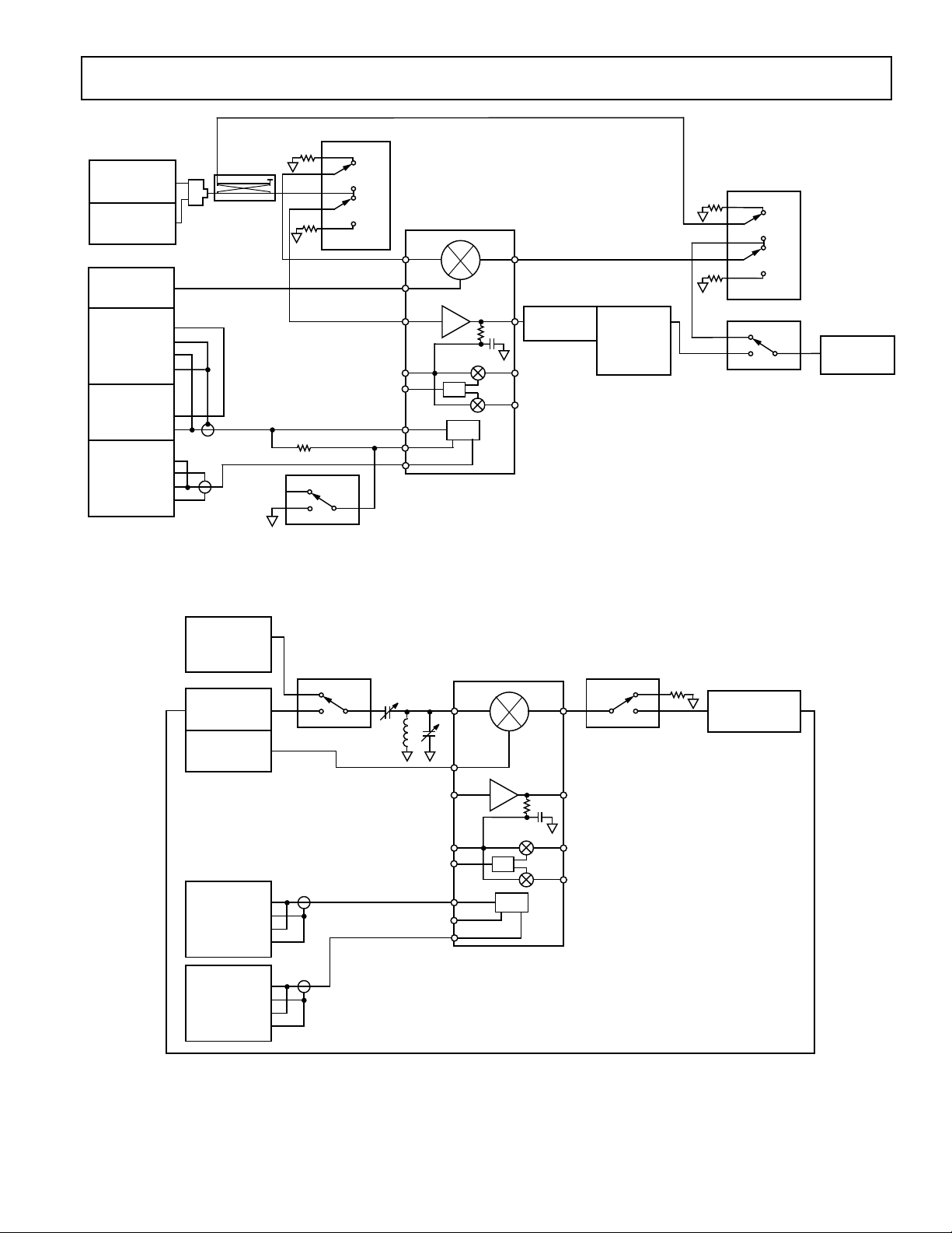
PRODUCT OVERVIEW
The AD607 provides most of the active circuitry required to
realize a complete low power, single-conversion superheterodyne receiver, or most of a double-conversion receiver, at input
frequencies up to 500 MHz, and with an IF of from 400 kHz to
12 MHz. The internal I/Q demodulators, and their associated
phase locked-loop, which can provide carrier recovery from the
IF, support a wide variety of modulation modes, including nPSK, n-QAM, and AM. A single positive supply voltage of 3 V
is required (2.7 V minimum, 5.5 V maximum) at a typical supply current of 8.5 mA at midgain. In the following discussion,
V
will be used to denote the power supply voltage, which will
P
be assumed to be 3 V.
Figure 33 shows the main sections of the AD607. It consists of a
variable-gain UHF mixer and linear four-stage IF strip, which
together provide a voltage controlled gain range of more than
90 dB; followed by dual demodulators, each comprising a multiplier followed by a 2-pole, 2 MHz low-pass filter; and driven by
a phase-locked loop providing the inphase and quadrature
clocks. An internal AGC detector is included, and the temperature stable gain control system provides an accurate RSSI capability. A biasing system with CMOS compatible power-down
completes the AD607.
Mixer
The UHF mixer is an improved Gilbert cell design, and can
operate from low frequencies (it is internally dc-coupled) up to
an RF input of 500 MHz. The dynamic range at the input of the
mixer is determined, at the upper end, by the maximum input
signal level of ±56 mV between RFHI and RFLO up to which
the mixer remains linear, and, at the lower end, by the noise
level. It is customary to define the linearity of a mixer in terms
of the 1 dB gain-compression point and third-order intercept,
which for the AD607 are –15 dBm and –8 dBm, respectively, in
a 50 Ω system.
Figure 32. Power Supply Current vs. Gain Control Voltage,
GREF = 1.5 V
LOIP
RFHI
RFLO
VPS1
VPS2
PRUP
MID-POINT
BIAS
GENERATOR
BIAS
GENERATOR
MXOP
VMID
COM1 COM2
BPF
IFHI
IFLO
Figure 33. Functional Block Diagram
VMID
PTAT
VOLTAGE
IFOP
AGC
DETECTOR
BPF OR
LPF
DMIP
AD607
VQFO
IOUT
FDIN
FLTR
QOUT
GAIN/RSSI
GREF
REV. 0
–13–
Page 14

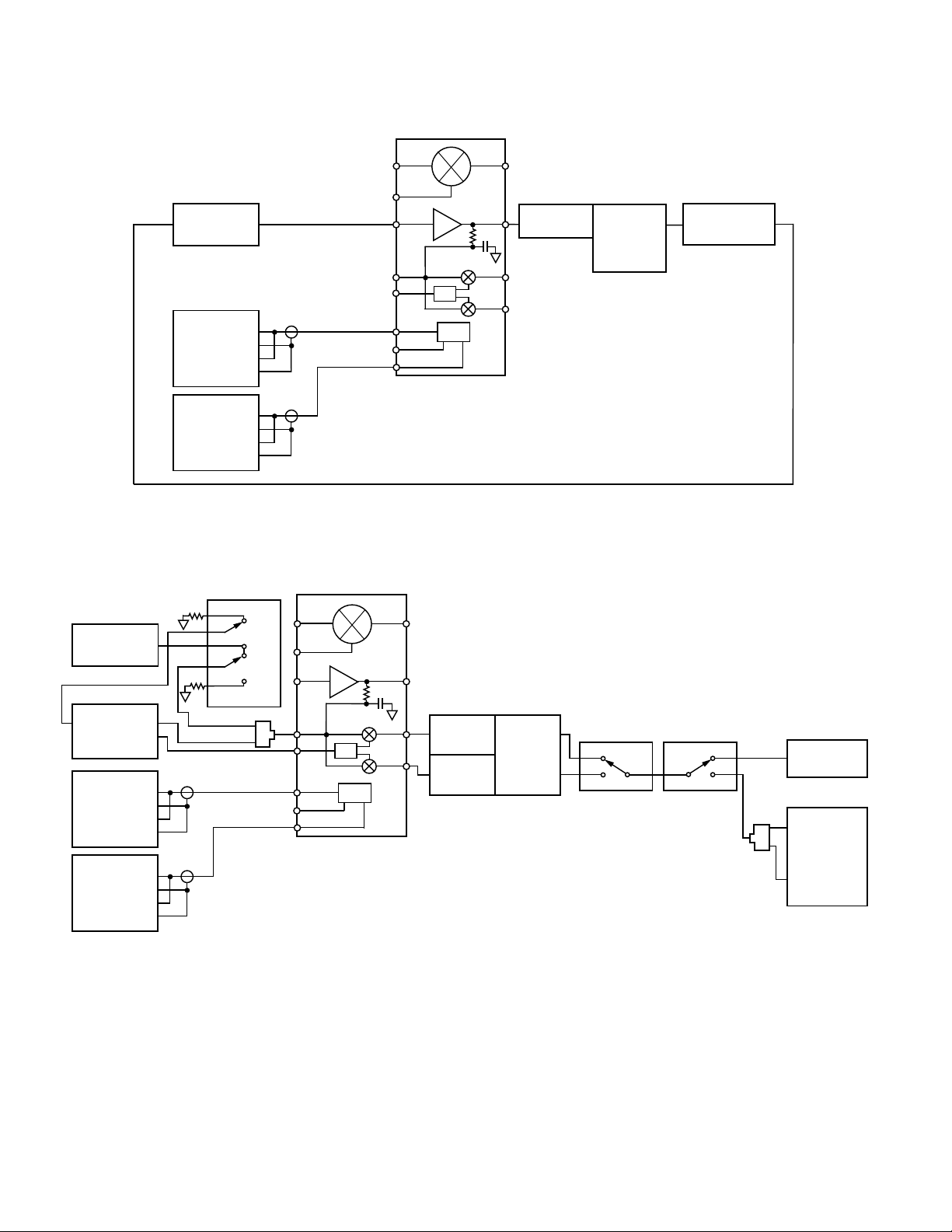
AD607
The mixer’s RF input port is differential, that is, pin RFLO is
functionally identical to RFHI, and these nodes are internally
biased; we will generally assume that RFLO is decoupled to ac
ground. The RF port can be modeled as a parallel RC circuit as
shown in Figure 34.
AD607
C2C1
RFHI
R
C
IN
L1
C3
C1, C2, L1: OPTIONAL MATCHING CIRCUIT
C3: COUPLES RFLO TO AC GROUND
RFLO
IN
Figure 34. Mixer Port Modeled as a Parallel RC Network;
an Optional Matching Network Is also Shown
The local oscillator (LO) input is internally biased at VP/2 via a
nominal 1000 Ω resistor internally connected from pin LOIP to
VMID. The LO interface includes a preamplifier which minimizes the drive requirements, thus simplifying the oscillator design and reducing LO leakage from the RF port. Internally, this
single-sided input is actually differential; the noninverting input
is referenced to pin VMID. The LO requires a single-sided drive
of ±50 mV, or –16 dBm in a 50 Ω system.
The mixer’s output passes through both a low-pass filter and a
buffer, which provides an internal differential to single-ended
signal conversion with a bandwidth of approximately 45 MHz.
Its output at pin MXOP is in the form of a single-ended current.
This approach eliminates the 6 dB voltage loss of the usual series termination by replacing it with shunt terminations at the
both the input and the output of the filter. The nominal conversion gain is specified for operation into a total IF bandpass filter
(BPF) load of 165 Ω, that is, a 330 Ω filter, doubly-terminated
as shown in Figure 33. Note that these loads are connected to
bias point VMID, which is always at the midpoint of the supply
(that is, V
/2).
P
The conversion gain is measured between the mixer input and
the input of this filter, and varies between 1.5 dB and 26.5 dB
for a 165 Ω load impedance. Using filters of higher impedance,
the conversion gain can always be maintained at its specified
value or made even higher; for filters of lower impedance, of say
Z
, the conversion gain will be lowered by 10 log10(165/ZO).
O
Thus, the use of a 50 Ω filter will result in a conversion gain that
is 5.2 dB lower. Figure 35 shows filter matching networks and
Table I lists resistor values.
MXOP
VMID
R2
8
9
BPF
R1
100nF
1nF
R3
100nF
10
IFHI
IFLO
11
Table I. AD607 Filter Termination Resistor Values for
Common IFs
Filter Filter Termination Resistor
IF Impedance Values1 for 24 dB of Mixer Gain
R1 R2 R3
450 kHz 1500 Ω 174 Ω 1330 Ω 1500 Ω
455 kHz 1500 Ω 174 Ω 1330 Ω 1500 Ω
6.5 MHz 1000 Ω 215 Ω 787 Ω 1000 Ω
10.7 MHz 330 Ω 330 Ω 0 Ω 330 Ω
NOTES
1
Resistor values were calculated such that R1+ R2 = Z
R1i (R2 + Z
FILTER
) = 165 Ω.
FILTER
and
The maximum permissible signal level at MXOP is determined
by both voltage and current limitations. Using a 3 V supply and
VMID at 1.5 V, the maximum swing is about ±1.3 V. To attain
a voltage swing of ±1 V in the standard IF filter load of 165 Ω
load requires a peak drive current of about ±6 mA, which is well
within the linear capability of the mixer. However, these upper
limits for voltage and current should not be confused with issues
related to the mixer gain, already discussed. In an operational
system, the AGC voltage will determine the mixer gain, and
hence the signal level at the IF input pin IFHI; it will always be
less than ±56 mV (–15 dBm into 50 Ω), which is the limit of
the IF amplifier’s linear range.
IF Amplifier
Most of the gain in the AD607 arises in the IF amplifier strip,
which comprises four stages. The first three are fully differential
and each has a gain span of 25 dB for the nominal AGC voltage
range. Thus, in conjunction with the mixer’s variable gain, the
total gain exceeds 90 dB. The final IF stage has a fixed gain of
20 dB, and it also provides differential to single-ended conversion.
The IF input is differential, at IFHI (noninverting relative to the
output IFOP) and IFLO (inverting). Figure 36 shows a simplified schematic of the IF interface. The offset voltage of this
stage would cause a large dc output error at high gain, so it is
nulled by a low-pass feedback path from the IF output, also
shown in Figure 25. Unlike the mixer output, the signal at IFOP
is a low-impedance single-sided voltage, centered at V
/2 by the
P
DC feedback loop. It may be loaded by a resistance as low as
50 Ω which will normally be connected to VMID.
AD607
LOOP
10kΩ
10kΩ
VMID
IFOP
IFHI
IFLO
OFFSET FEEDBACK
Figure 36. Simplified Schematic of the IF Interface
Figure 35. Suggested IF Filter Matching Network. The
Values of R1 and R2 Are Selected to Keep the Impedance
at Pin MXOP at 165
Ω
–14–
REV. 0
Page 15

AD607
The IF’s small-signal bandwidth is approximately 45 MHz from
IFHI and IFLO through IFOP. The peak output at IFOP is
±560 mV at V
= 3 V and ±400 mV at the minimum V
P
of
P
2.7 V. This allows some headroom at the demodulator inputs
(pin DMIP), which accept a maximum input of ± 150 mV for
IFs > 3 MHz and ±75 mV for IFs ≤ 3 MHz (at IFs ≤ 3 MHz,
the drive to the demodulators must be reduced to avoid saturating the output amplifiers with higher order mixing products that
are no longer removed by the onboard low-pass filters).
If the internal AGC detector is used, the IF output will be at an
amplitude of V
/10, that is, ±300 mV for VP = 3 V. This ±300
P
mV level requires the insertion of 6 dB of post-IF filter loss between IFOP and DMIP to avoid overloading the demodulators;
often, a simple RC low-pass filter with its corner frequency at
the IF will suffice.
Since there is no band-limiting in the IF strip, the outputreferred noise can be quite high; in a typical application and at a
gain of 75 dB it is about 100 mV rms, making post-IF filtering
desirable. IFOP may be also used as an IF output for driving an
A/D converter, external demodulator, or external AGC detector.
Figure 37 shows methods of matching the optional second IF
filter.
VPOS
AD607
DMIP
IFOP
R
T
BPF
2R
T
2R
T
a. Biasing DMIP from Power Supply (Assumes BPF AC
Coupled Internally)
AD607
IFOP
R
T
BPF
The gain control scaling is proportional to the reference voltage
applied to the pin GREF. When this pin is tied to the midpoint
of the supply (VMID), the scale is nominally 20 mV/dB (50 dB/
V) for V
= 3 V. Under these conditions, the lower 80 dB of
P
gain range (mixer plus IF) corresponds to a control voltage of
0.4 V ≤ V
≤ 2.0 V. The final centering of this 1.6 V range de-
G
pends on the insertion losses of the IF filters used. More generally, the gain scaling using these connections is V
/150 (volts
P
per dB), so becomes 33.3 mV/dB (30 dB/V) using a 5 V supply,
with a proportional change in the AGC range, to 0.33 V ≤
V
≤ 3 V, Table II lists gain control voltages and scale factors
G
for power supply voltages from 2.7 V to 5.5 V.
Alternatively, pin GREF can be tied to an external voltage
reference, V
, provided, for example, by an AD1582 (2.5 V)
R
or AD1580 (1.21 V) voltage reference, to provide supplyindependent gain scaling of V
/75 (volts per dB). When using
R
the Analog Devices’ AD7013 and AD7015 baseband converters,
the external reference may also be provided by the reference
output of the baseband converter (Figure 38). For example, the
AD7015 baseband converter provides a V
of 1.23 V; when
R
connected to GREF the gain scaling is 16.4 mV/dB (60 dB/V).
An auxiliary DAC in the AD7015 can be used to generate the
MGC voltage. Since it uses the same reference voltage, the numerical input to this DAC provides an accurate RSSI value in
digital form, no longer requiring the reference voltage to have
high absolute accuracy.
C
AD7013 OR
AD7015
IADC
QADC
IADC
QADC
REFOUT
BYPASS
AUX DAC
(AD7015)
(AD7013)
AD607
QOUT
GREF
GAIN/RSSI
IOUT
VMID
R
R
C
10nF
1nF
DMIP
R
VMID
C
T
BYPASS
b. Biasing DMIP from VMID (Assumes BPF AC Coupled
Internally)
Figure 37. Input and Output Matching of the Optional
Second IF Filter
Gain Scaling and RSSI
The AD607’s overall gain, expressed in decibels, is linear-in-dB
with respect to the AGC voltage V
gain of all sections is maximum when V
progressively up to V
limit V
– 0.8 V). The gain of all stages changes in parallel. The
P
= 2.2 V (for VP = 3 V; in general, up to a
G
at pin GAIN/RSSI. The
G
is zero, and reduces
G
AD607 features temperature-compensation of the gain scaling.
Note that GAIN/RSSI pin is either an MGC input, when the
gain is controlled by some external means, or an RSSI output,
when the internal AGC detector is used.
REV. 0
–15–
Figure 38. Interfacing the AD607 to the AD7013 or AD7015
Baseband Converters
I/Q Demodulators
Both demodulators (I and Q) receive their inputs at pin DMIP.
Internally, this single-sided input is actually differential; the
noninverting input is referenced to pin VMID. Each demodulator comprises a full-wave synchronous detector followed by a
2 MHz, two-pole low-pass filter, producing single-sided outputs
at pins IOUT and QOT. Using the I and Q demodulators for
IFs above 12 MHz is precluded by the 400 kHz to 12 MHz
response of the PLL used in the demodulator section. Pin DMIP
requires an external bias source at V
/2; Figure 39 shows sug-
P
gested methods.
Outputs IOUT and QOUT are centered at V
/2 and can swing
P
up to ±1.23 V even at the low supply voltage of 2.7 V. They
can therefore directly drive the RX ADCs in the AD7015
baseband converter, which require an amplitude of 1.23 V to
fully load them when driven by a single-sided signal. The conversion gain of the I and Q demodulators is 18 dB (X8), requiring a maximum input amplitude at DMIP of ± 150 mV for IFs >
3 MHz.
Page 16

AD607
SEQUENTIAL
PHASE
DETECTOR
VARIABLE-
FREQUENCY
QUADRATURE
OSCILLATOR
90°
Q-CLOCK
(ECL OUTPUTS)
I-CLOCK
REFERENCE CARRIER
(FDIN AFTER LIMITING)
U
D
IU~
40µA
C
R
V
F
F
R
I
D
~
40µA
VPOS
AD607
IFOP
DMIP
R
T
BPF
2R
T
2R
T
a. Biasing DMIP from Power Supply (Assumes BPF AC
Coupled Internally)
AD607
IFOP
DMIP
DMIP
R
T
BPF
R
T
C
BYPASS
b. Biasing DMIP from VMID (Assumes BPF AC Coupled
Internally)
Figure 39. Suggested Methods for Biasing Pin DMIP
/2
at V
P
For IFs < 3 MHz, the on-chip low-pass filters (2 MHz cutoff)
do not attenuate the IF or feedthrough products; thus, the maximum input voltage at DMIP must be limited to ± 75 mV to allow sufficient headroom at the I and Q outputs for not only the
desired baseband signal but also the unattenuated higher-order
demodulation products. These products can be removed by an
external low-pass filter. In the case of IS54 applications using a
455 kHz IF and the AD7013 baseband converter, a simple
1-pole RC filter with its corner above the modulation bandwidth
is sufficient to attenuate undesired outputs.
Phase-Locked Loop
The demodulators are driven by quadrature signals that are provided by a variable frequency quadrature oscillator (VFQO),
phase locked to a reference signal applied to pin FDIN. When
this signal is at the IF, inphase and quadrature baseband outputs are generated at IOUT and QOUT, respectively. The
quadrature accuracy of this VFQO is typically –1.2° at
10.7 MHz. The PLL uses a sequential-phase detector that
comprises low power emitter-coupled logic and a charge pump
(Figure 40).
Figure 40. Simplified Schematic of the PLL and
Quadrature VCO
The reference signal may be provided from an external source,
in the form of a high-level clock, typically a low level signal
(±400 mV) since there is an input amplifier between FDIN and
the loop’s phase detector. For example, the IF output itself can
be used by connecting DMIP to FDIN, which will then provide automatic carrier recover for synchronous AM detection
and take advantage of any post-IF filtering. Pin FDIN must be
biased at V
/2; Figure 41 shows suggested methods.
P
The VFQO operates from 400 kHz to 12 MHz and is controlled by the voltage between VPOS and FLTR. In normal operation, a series RC network, forming the PLL loop filter, is
connected from FLTR to ground. The use of an integral
sample-hold system ensures that the frequency-control voltage
on pin FLTR remains held during power-down, so reacquisition
of the carrier typically occurs in 16.5 µs.
In practice, the probability of a phase mismatch at power-up is
high, so the worst-case linear settling period to full lock needs
to be considered in making filter choices. This is typically 16.5 µs
at an IF of 10.7 MHz for a ±100 mV signal at DMIP and
FDIN.
NOTE
Maximum gain occurs for gain control voltage = 0 V.
Table II. AD607 Gain and Manual Gain Control Voltage vs. Power Supply Voltage
Power Supply GREF Gain Control
Voltage (= VMID) Scale Factor Scale Factor Voltage Input Range
(V) (V) (dB/V) (mV/dB) (V)
2.7 1.35 55.56 18.00 0.360–1.800
3.0 1.5 50.00 20.00 0.400–2.000
3.5 1.75 42.86 23.33 0.467–2.333
4.0 2.0 37.50 26.67 0.533–2.667
4.5 2.25 33.33 30.00 0.600–3.000
5.5 2.75 27.27 36.67 0.733–3.667
5.0 2.5 30.00 33.33 0.667–3.333
–16–
REV. 0
Page 17

AD607
Bias System
The AD607 operates from a single supply, VP, usually of 3 V, at
a typical supply current of 8.5 mA at midgain and T = 27°C,
corresponding to a power consumption of 25 mW. Any voltage
from 2.7 V to 5.5 V may be used.
The bias system includes a fast-acting active-high CMOScompatible power-up switch, allowing the part to idle at 550 µA
when disabled. Biasing is proportional-to-absolute-temperature
(PTAT) to ensure stable gain with temperature.
An independent regulator generates a voltage at the midpoint of
the supply (V
/2) which appears at the VMID pin, at a low im-
P
pedance. This voltage does not shut down, ensuring that the
major signal interfaces (e.g., mixer-to-IF and IF-to-demodulators) remain biased at all times, thus minimizing transient disturbances at power-up and allowing the use of substantial
decoupling capacitors on this node. The quiescent consumption
of this regulator is included in the idling current.
EXTERNAL
FREQUENCY
REFERENCE
VPOS
50kΩ
50kΩ
AD607
FDIN
a. Biasing FDIN from Supply when Using
External Frequency Reference
AD607
EXTERNAL
FREQUENCY
REFERENCE
50kΩ
C
BYPASS
FDIN
VMID
USING THE AD607
In this section, we will focus on a few areas of special importance and include a few general application tips. As is true of
any wideband high gain component, great care is needed in PC
board layout. The location of the particular grounding points
must be considered with due regard to possibility of unwanted
signal coupling, particularly from IFOP to RFHI or IFHI or both.
The high sensitivity of the AD607 leads to the possibility that
unwanted local EM signals may have an effect on the performance. During system development, carefully-shielded test assemblies should be used. The best solution is to use a fullyenclosed box enclosing all components, with the minimum
number of needed signal connectors (RF, LO, I and Q outputs)
in miniature coax form.
The I and Q output leads can include small series resistors
(about 100 Ω) inside the shielded box without significant loss of
performance, provided the external loading during testing is
light (that is, a resistive load of more than 20 kΩ and capacitances of a few picofarads). These help to keep unwanted RF
emanations out of the interior.
The power supply should be connected via a through-hole capacitor with a ferrite bead on both inside and outside leads.
Close to the IC pins, two capacitors of different value should be
used to decouple the main supply (V
) and the midpoint supply
P
pin, VMID. Guidance on these matters is also generally included in applications schematics.
Gain Distribution
As in all receivers, the most critical decisions in effectively using
the AD607 relate to the partitioning of gain between the various
subsections (Mixer, IF Amplifier, Demodulators) and the placement of filters, so as to achieve the highest overall signal-tonoise ratio and lowest intermodulation distortion.
Figure 42 shows the main RF/IF signal path at maximum and
minimum signal levels.
b. Biasing FDIN from VMID when Using
External Frequency Reference
Figure 41. Suggested Methods for Biasing Pin FDIN
at V
/2
P
I
±54mV
MAX INPUT
RFHI
CONSTANT
–16dBm
(±50mV)
MAX OUTPUT
LOIP
±1.3V
±54mV
MAX INPUT
MXOP IFHI
IF BPF IF BPF
330Ω330Ω
(TYPICAL
IMPEDANCE)
MAX OUTPUT
(LOCATION OF OPTIONAL
SECOND IF FILTER)
±560mV
(VMID)
±154mV
MAX INPUT
DMIPIFOP
Q
Figure 42. Signal Levels for Minimum and Maximum Gain
REV. 0
–17–
±1.23V
MAX OUTPUT
IOUT
QOUT
Page 18

AD607
As noted earlier, the gain in dB is reduced linearly with the voltage V
on the GAIN pin. Figure 43 shows how the mixer and
G
IF strip gains vary with V
(1.5 V) and a supply voltage of 3 V is used. Figure 44 shows
how these vary when GREF is connected to a 1.23 V reference.
90dB
80dB
70dB
60dB
50dB
40dB
30dB
20dB
10dB
0dB
0.4V 1.8V
01V2V
Figure 43. Gain Distribution for GREF = 1.5 V
90dB
80dB
70dB
60dB
50dB
40dB
30dB
20dB
10dB
0dB
0.328V 1.64V
01V2V
Figure 44. Gain Distribution for GREF = 1.23 V
Using the Internal AGC Detector
The AD607 includes a detector cell at the output of the IF amplifier that allows it to provide its own AGC and output-leveling
function in receiver applications where DSP support is not
needed. It is only necessary to connect a filter capacitor between
the GAIN pin and ground to invoke this feature. The voltage
appearing on this pin may then be used as an RSSI output, with
the scaling discussed earlier; note particularly that the voltage on
GREF continues to determine this scaling.
Figure 45 shows a simplified schematic of the detector. Transistor Q2 remains cut off by a 300 mV bias (when V
eral, ≈ V
/10) until the positive tip of the IF waveform causes
P
it to briefly conduct, charging the AGC filter capacitor C
a positive direction. The voltage across this capacitor is V
when GREF is connected to VMID
G
(67.5dB)
IF GAIN
(21.5dB)
(67.5dB)
(21.5dB)
NORMAL OPERATING RANGE
MIXER GAIN
NORMAL OPERATING RANGE
IF GAIN
MIXER GAIN
(7.5dB)
2.2V
V
g
(7.5dB)
(1.5dB)
= 3 V; in gen-
P
(1.5dB)
V
g
AGC
.
G
in
30µA
˜
4.5µA
ZERO
1.5V + 316mV
TO INTERNAL
GAIN CONTROL
AVERAGE OF IC2 IS
FORCED TO 4.5µA BY
INTEGRATION IN CAGC
LAST IF STAGE
1.5V
IF OUTPUT
IFOP
Q1 Q2
COMM
77µA
GAIN
4.5µA
(INT)
I
C
CAGC
(EXT)
2
Figure 45. Simplified Schematic of AGC Detector
Acting against this is an internally generated 4.5 µA pull-down
current, which operates to within a few millivolts of ground. As
V
the voltage at the GAIN/RSSI pin, rises, the gain falls, so re-
G,
ducing the amplitude of the IF output and reducing the amplitude of the current spike in Q2; eventually a point is reached
where its average collector current is balanced by the pull-down
current, and the charging ceases. It will be apparent that the
loop filter is essentially a perfect integrator.
This simple system can be used because the input impedance of
the gain-control system, also internally tied to the GAIN/RSSI
pin, is several megohms, and its bias current is small. The voltage V
may be used as an RSSI output; however, if it is to be
G
heavily loaded, a buffer amplifier must be used.
Note that, unlike a post-demodulation AGC detector (via DSP),
this scheme responds to signal plus noise. Thus, when operating
at high gains, the AGC loop will “see” a substantial output at
the IFOP node, even though a filter may be added by the user
between the pins IFOP and DMIP. This will trick the loop into
lowering the gain until the composite output signal (IF plus
noise) reaches the reference level and satisfies the averagecurrent requirement. In these circumstances, the wanted signal
will be smaller than expected. Thus, the internal AGC system
will result in a slight compression of the demodulated output for
very small signal levels.
AGC Discharge Time
The discharge current is approximately 4.5 µA; thus, to restore
gain in the event of a rapid drop-out requires a time of
T = C × V
/4.5 µA. Using a 1 nF capacitor, and noting that an
G
80 dB gain change corresponds to 1.6 V, the discharge time is
355 µs. Note, however, that when GREF is tied to a different
value, the scaling changes. For GREF = 1.23 V, the scale factor
is 16.4 mV/dB, 80 dB corresponds to a 1.312 V change, and the
discharge time decreases to 290 µs.
V
could also be expressed in dB: with a scaling of 20 mV/dB, it
G
works out to T = C × P × 44,000, where P is the change in input
power, expressed in dB. Thus, using C = 1 nF, checking the
time needed for 80 dB we get T = 355 µs. For the case where
the scaling is 16.4 mV/dB, T = C × P × 36,000.
The AD607’s AGC detector delivers only one brief charging
pulse per cycle of the IF. At a 10.7 MHz IF, for example, this is
every 93 ns. When the AGC system is in equilibrium, this pulse
–18–
REV. 0
Page 19

AD607
of current exactly balances the 4.5 µA discharge current. (It
makes no difference what the actual value of V
is at that point,
G
since the AGC filter is an integrator.)
Thus, at 20 mV/dB
IT
V
RIPPLE
=
4.5 µA × 93 ns
=
C
1 nF
= 0. 42 mV
This corresponds to 0.021 dB, and the ripple will modulate the
gain by that amount over each cycle. The effect of such modulation on the signal is hard to quantify, but it roughly translates to
a 2% amplitude modulation. Also, the gain ripple depends on
the scale factor. For this example, at GREF = 1.23 V and a
16.4 mV/dB scale factor, the gain ripple increases to 0.025 dB.
AGC Charge Time
When the gain is too high, the IF amplifier will be overdriven to
produce a square wave output (roughly) of ±560 mV. If perfectly square and time- and amplitude-symmetric, this would be
sliced at the 300 mV level to generate a current of 76 µA/2, or
38 µA. After subtracting the 4.5 µA, we should have about 33 µA.
In fact, the maximum ramp-up current is about 20 µA, because
the waveform is not a crisp square wave (and as the loop approaches equilibrium it is more nearly sinusoidal). Thus, the
ramp-up rate is 20/4.5 = 4.4 times faster than the discharge rate.
In our example, a 1.6 V change will require about 1.5 ms using
C = 1 nF.
Applications Hints
Do not place a resistor from Pin 12 to Ground: The resistor
converts the integrator—ideal for AGC—into a low-pass filter.
An integrator needs no input to sustain a given output; a low-
pass filter does. This “input” is an INCREASED AMPLITUDE
required at IFOP. The AGC loop thus does not level the output
at IFOP.
Reasons for Using a Larger AGC Capacitor
1. In applications where gain modulation may be troublesome,
raise the capacitor from 1 nF to 2.7 nF; the 80 dB slew time
(at 20 mV/dB) is now close to 1 ms.
2. As the IF is lowered, the capacitor must be increased accordingly if gain ripple is to be avoided. Thus, to achieve the
same ripple at 455 kHz requires the 1 nF capacitor to be increased to 0.022 µF.
3. In AM applications, the AGC loop must not track the modulation envelope. The objective should be that the gain should
not vary by more than the amount required to introduce, say,
1% THD distortion at the lowest modulation frequency, say,
300 Hz. Note that in AM applications it is the modulation
bandwidth that determines the required AGC filter capacitor, not the IF.
4. In some applications, even slower AGC may be desired than
that required to prevent modulation tracking.
AD607 EVALUATION BOARD
The AD607 evaluation board (Figures 46 and 47) consists of an
AD607, ground plane, I/O connectors, and a 10.7 MHz bandpass filter. The RF and LO ports are terminated in 50 Ω to
provide a broadband match to external signal generators to allow a choice of RF and LO input frequencies. The IF filter is at
10.7 MHz and has 330 Ω input and output terminations; the
board is laid out to allow the user to substitute other filters for
other IFs.
FDIN
VPOS
GND
FDIN
PRUP
LO
RF
C18
SHORT
R14
C17
51.1Ω
10nF
MOD FOR LARGE MAGNITUDE
AC COUPLED INPUT
C13 0
C14 0
VMID
R8
51.1Ω
R12
OPEN
C15
0.1µF
R15
50kΩ
R7
51.1Ω
R6
51.1Ω
C11
10nF
C10
1nF
332Ω
332Ω
R13
50kΩ
JUMPER
0.1µF
C9
1nF
R5
R3
C12
VPOS
FDIN
R10
4.99kΩ
R9
0
R11
OPEN
C16
1nF
JUMPER
R4
0
C7
1nF
AD607 EVALUATION BOARD
(AS RECEIVED)
FDIN
COM1
PRUP
LOIP
RFLO
RFHI
GREF
MXOP
VMID
IFHI
AD607
FDIN
C1
VPS1
FLTR
IOUT
QOUT
VPS2
DMIP
IFOP
COM2
GAIN
IFLO
RSOURCE
0.1µF
R1
1kΩ
C2
0.1µF
R2
316Ω
C6
0.1µF
C8
0.1µF
ANYTHING
C20
R19
SHORT
MOD FOR DC COUPLED INPUT
C19
C3
10nF
I
C5
1nF
C4
47pF
VMID
OPEN
R16
OPEN
R17
Q
IF
RSSI
R18
OPEN
VPOS
FDIN
REV. 0
Figure 46. Evaluation Board
–19–
Page 20

AD607
Figure 47. Evaluation Board Layout
–20–
REV. 0
Page 21

AD607
The board provides SMA connectors for the RF and LO port
inputs, the demodulated I and Q outputs, the manual gain control (MGC) input, the PLL input, and the power-up input. In
addition, the IF output is also available at an SMA connector;
Table III. AD607 Evaluation Board Input and Output Connections
Reference Connector Approximate
Designation Type Description Coupling Signal Level Comments
J1 SMA Frequency DC ±400 mV This pin needs to be biased at VMID
Detector Input and ac coupled when driven by an
J2 SMA Power Up DC CMOS Logic Tied to Positive Supply by Jumper J10.
J3 SMA LO Input AC –16 dBm Input is terminated in 50 Ω.
J4 SMA RF Input AC –15 dBm max Input is terminated in 50 Ω.
J5 SMA MGC Input DC 0.4 V to 2.0 V Jumper is set for Manual Gain Control
or (3 V Supply) Input; See Table I for Control Voltage
RSSI Output (GREF = VMID) Values.
J6 SMA IF Output AC NA This signal level depends on the
J7 SMA Q Output AC NA This signal level depends on the
J8 SMA I Output AC NA This signal level depends on the
J9 Jumper Ties GREF NA NA Sets gain-control Scale Factor (SF);
to VMID SF = 75/VMID in dB/V, where
J10 Jumper Ties Power-Up NA NA Remove to test Power Up/Down.
to Positive
Supply
T1 Terminal Pin Power Supply DC DC 2.7 V to 5.5 V
Positive Input Draws 8.5 mA at
(VPS1, VPS2) midgain connection.
T2 Terminal Pin Power Supply DC 0 V
Return (GND)
this may be connected to the PLL input for carrier recovery to
realize synchronous AM and FM detection via the I and Q demodulators, respectively. Table III lists the AD607 Evaluation
Board’s I/O Connectors and their functions.
external signal generator.
Level Input
(±50 mV)
(±54 mV)
AD607’s gain setting.
AD607’s gain setting.
AD607’s gain setting.
VMID = VPOS/2.
REV. 0
–21–
Page 22

AD607
In operation (Figure 48), the AD607 evaluation board draws
about 8.5 mA at midgain (59 dB). Use high impedance probes
to monitor signals from the demodulated I and Q outputs and
the IF output. The MGC voltage should be set such that the
signal level at DMIP does not exceed ± 150 mV; signal levels
above this will overload the I and Q demodulators. The insertion loss between IFOP and DMIP is typically 3 dB if a simple
low-pass filter (R8 and C2) is used and higher if a reverseterminated bandpass filter is used.
HP 6632A
PROGRAMMABLE
POWER SUPPLY
2.7V–6V
FLUKE 6082A
SYNTHESIZED
SIGNAL GENERATOR
240 MHz
RF
HP 8656A
SYNTHESIZED
SIGNAL GENERATOR
240.02 MHz
MCL
ZFSC–2–1
COMBINER
Σ
If the AD607’s internal AGC detector is used, then the GAIN/
RSSI (Pin 12) becomes an output and the RSSI voltage appears
across C12, which serves as an integrating capacitor. This voltage must be monitored by a high impedance (100 kΩ minimum)
probe. The internal AGC loop holds the IF voltage at IFOP
(Pin 14) at ±300 mV; in this application, about 6 dB of attenuation is needed between pins IFOP and DMIP to avoid overloading the I and Q demodulators.
HP 3326
SYNTHESIZED
SIGNAL GENERATOR
10.710 MHz
VPOS
AD607
EVALUATION
BOARD
FDIN
I OUTPUT
Q OUTPUT
MGCLO
TEKTRONIX
11402A
OSCILLOSCOPE
WITH 11A32
PLUGIN
HP 9920
IEEE CONTROLLER
HP9121
DISK DRIVE
HP 8656A
SYNTHESIZED
SIGNAL GENERATOR
229.3 MHz
Figure 48. Evaluation Board Test Setup
DATA PRECISION
DVC8200
PROGRAMMABLE
VOLTAGE SOURCE
IEEE –488 BUS
–22–
REV. 0
Page 23

OUTLINE DIMENSIONS
Dimensions shown in inches and (mm).
20-Pin Plastic SSOP (RS-20)
AD607
20
PIN 1
1
0.295 (7.50)
0.271 (6.90)
0.008 (0.203)
0.002 (0.050)
1. LEAD NO. 1 IDENTIFIED BY A DOT.
2. LEADS WILL BE EITHER TIN PLATED OR SOLDER DIPPED
IN ACCORDANCE WITH MIL-M-38510 REQUIREMENTS
0.0256 (0.65)
BSC
11
0.205 (5.207)
10
0.066 (1.67)
0.009 (0.229)
0.005 (0.127)
0.212 (5.38)
0.07 (1.78)
0.311 (7.9)
0.301 (7.64)
8°
0°
0.037 (0.94)
0.022 (0.559)
REV. 0
–23–
Page 24

C2047–10–7/95
–24–
PRINTED IN U.S.A.
 Loading...