

Page 1
LVDT Signal
a
FEATURES
Single Chip Solution, Contains Internal Oscillator and
Voltage Reference
No Adjustments Required
Insensitive to Transducer Null Voltage
Insensitive to Primary to Secondary Phase Shifts
DC Output Proportional to Position
20 Hz to 20 kHz Frequency Range
Single or Dual Supply Operation
Unipolar or Bipolar Output
Will Operate a Remote LVDT at Up to 300 Feet
Position Output Can Drive Up to 1000 Feet of Cable
Will Also Interface to an RVDT
Outstanding Performance
Linearity: 0.05% of FS max
Output Voltage: 611 V min
Gain Drift: 50 ppm/8C of FS max
Offset Drift: 50 ppm/8C of FS max
PRODUCT DESCRIPTION
The AD598 is a complete, monolithic Linear Variable Differential Transformer (LVDT) signal conditioning subsystem. It is
used in conjunction with LVDTs to convert transducer mechanical position to a unipolar or bipolar dc voltage with a high
degree of accuracy and repeatability. All circuit functions are
included on the chip. With the addition of a few external passive
components to set frequency and gain, the AD598 converts the
raw LVDT secondary output to a scaled dc signal. The device
can also be used with RVDT transducers.
The AD598 contains a low distortion sine wave oscillator to
drive the LVDT primary. The LVDT secondary output consists
of two sine waves that drive the AD598 directly. The AD598
operates upon the two signals, dividing their difference by their
sum, producing a scaled unipolar or bipolar dc output.
The AD598 uses a unique ratiometric architecture (patent pending) to eliminate several of the disadvantages associated with
traditional approaches to LVDT interfacing. The benefits of this
new circuit are: no adjustments are necessary, transformer null
voltage and primary to secondary phase shift does not affect system accuracy, temperature stability is improved, and transducer
interchangeability is improved.
The AD598 is available in two performance grades:
Grade Temperature Range Package
AD598JR 0°C to +70°C 20-Pin Small Outline (SOIC)
AD598AD –40°C to +85°C 20-Pin Ceramic DIP
It is also available processed to MIL-STD-883B, for the military
range of –55°C to +125°C.
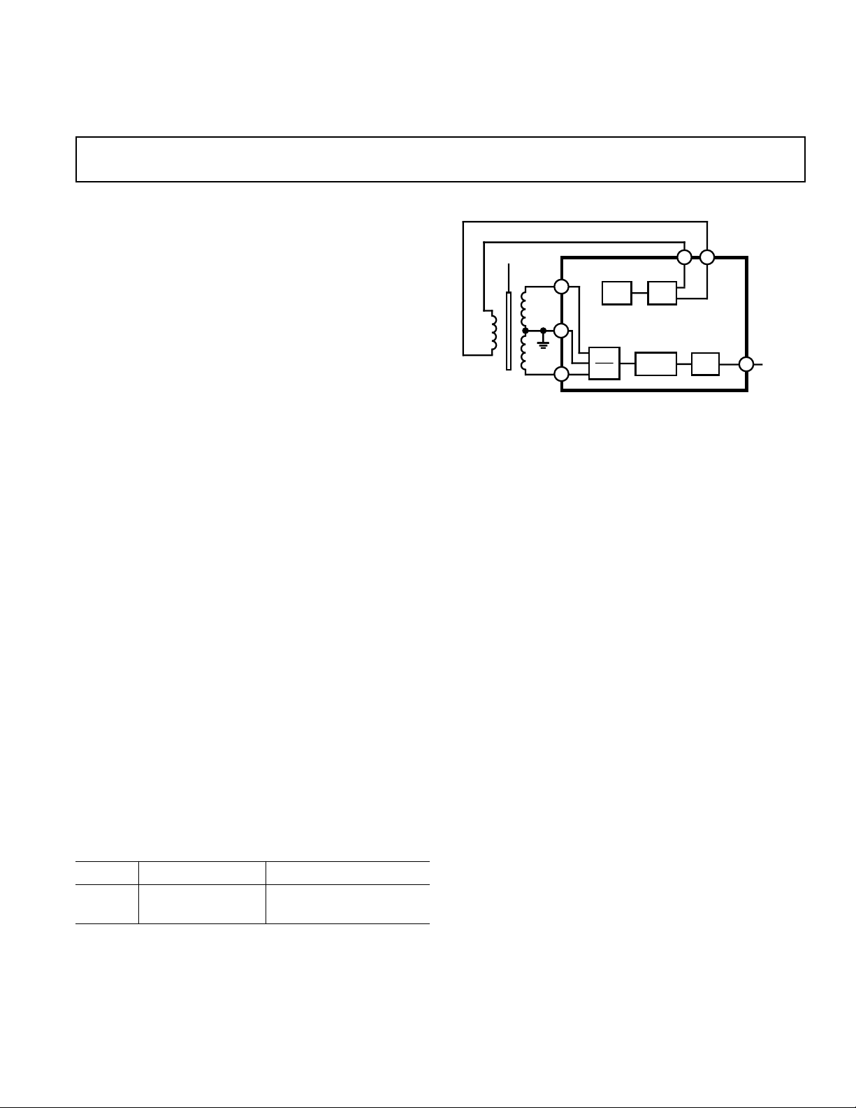
Conditioner
AD598
FUNCTIONAL BLOCK DIAGRAM
EXCITATION (CARRIER)
23
V
A
11
17
LVDT
PRODUCT HIGHLIGHTS
10
V
B
A–B
A+B
OSC
1. The AD598 offers a monolithic solution to LVDT and
RVDT signal conditioning problems; few extra passive components are required to complete the conversion from mechanical position to dc voltage and no adjustments are
required.
2. The AD598 can be used with many different types of
LVDTs because the circuit accommodates a wide range of
input and output voltages and frequencies; the AD598 can
drive an LVDT primary with up to 24 V rms and accept secondary input levels as low as 100 mV rms.
3. The 20 Hz to 20 kHz LVDT excitation frequency is determined by a single external capacitor. The AD598 input signal need not be synchronous with the LVDT primary drive.
This means that an external primary excitation, such as the
400 Hz power mains in aircraft, can be used.
4. The AD598 uses a ratiometric decoding scheme such that
primary to secondary phase shifts and transducer null voltage
have absolutely no effect on overall circuit performance.
5. Multiple LVDTs can be driven by a single AD598, either in
series or parallel as long as power dissipation limits are not
exceeded. The excitation output is thermally protected.
6. The AD598 may be used in telemetry applications or in hostile environments where the interface electronics may be remote from the LVDT. The AD598 can drive an LVDT at
the end of 300 feet of cable, since the circuit is not affected
by phase shifts or absolute signal magnitudes. The position
output can drive as much as 1000 feet of cable.
7. The AD598 may be used as a loop integrator in the design of
simple electromechanical servo loops.
AMP
FILTER
AD598
AMP
V
16
OUT
REV. A
Information furnished by Analog Devices is believed to be accurate and
reliable. However, no responsibility is assumed by Analog Devices for its
use, nor for any infringements of patents or other rights of third parties
which may result from its use. No license is granted by implication or
otherwise under any patent or patent rights of Analog Devices.
One Technology Way, P.O. Box 9106, Norwood, MA 02062-9106, U.S.A.
Tel: 617/329-4700 Fax: 617/326-8703
Page 2

(typical @ +258C and 615 V dc, C1 = 0.015 mF, R2 = 80 kV, RL = 2 kV,
AD598–SPECIFICATIONS
unless otherwise noted. See Figure 7.)
AD598J AD598A
Parameter Min Typ Max Min Typ Max Unit
V
A–VB
=
VA+V
×500 µA × R2
B
V
TRANSFER FUNCTION
OVERALL ERROR
T
to T
MIN
MAX
2
1
V
OUT
0.6 2.35 0.6 1.65 % of FS
SIGNAL OUTPUT CHARACTERISTICS
Output Voltage Range (T
Output Current (T
Short Circuit Current 20 20 mA
Nonlinearity
Gain Error
Gain Drift 20 6100 20 650 ppm/°C of FS
Offset
4
5
3
(T
MIN
MIN
to T
Offset Drift 7 6200 7 650 ppm/°C of FS
Excitation Voltage Rejection
to T
MIN
to T
MAX
)756500 75 6500 ppm of FS
MAX
) 611 611 V
MAX
)86mA
0.4 61 0.4 61 % of FS
0.3 61 0.3 61 % of FS
6
100 100 ppm/dB
Power Supply Rejection (± 12 V to ±18 V)
PSRR Gain (T
PSRR Offset (T
MIN
MIN
to T
to T
) 300 100 400 100 ppm/V
MAX
) 100 15 200 15 ppm/V
MAX
Common-Mode Rejection (± 3 V)
CMRR Gain (T
CMRR Offset (T
Output Ripple
to T
MIN
MIN
7
) 100 25 200 25 ppm/V
MAX
to T
) 100 6 200 6 ppm/V
MAX
4 4 mV rms
EXCITATION OUTPUT CHARACTERISTICS (@ 2.5 kHz)
Excitation Voltage Range 2.1 24 2.1 24 V rms
Excitation Voltage
(R1 = Open)
(R1 = 12.7 kΩ)
(R1 = 487 Ω)
Excitation Voltage TC
8
8
8
9
1.2 2.1 1.2 2.1 V rms
2.6 4.1 2.6 4.1 V rms
14 20 14 20 V rms
600 600 ppm/°C
Output Current 30 30 mA rms
T
MIN
to T
MAX
12 12 mA rms
Short Circuit Current 60 60 mA
DC Offset Voltage (Differential, R1 = 12.7 kΩ)
T
MIN
to T
MAX
30 6100 30 6100 mV
Frequency 20 20k 20 20k Hz
Frequency TC, (R1 = 12.7 kΩ) 200 200 ppm/°C
Total Harmonic Distortion –50 –50 dB
SIGNAL INPUT CHARACTERISTICS
Signal Voltage 0.1 3.5 0.1 3.5 V rms
Input Impedance 200 200 kΩ
Input Bias Current (AIN and BIN) 1 5 1 5 µA
Signal Reference Bias Current 2 10 2 10 µA
Excitation Frequency 0 20 0 20 kHz
POWER SUPPLY REQUIREMENTS
Operating Range 13 36 13 36 V
Dual Supply Operation (±10 V Output) ±13 ±13 V
Single Supply Operation
0 to +10 V Output 17.5 17.5 V
0 to –10 V Output 17.5 17.5 V
Current (No Load at Signal and Excitation Outputs) 12 15 12 15 mA
T
MIN
to T
MAX
16 18 mA
TEMPERATURE RANGE
JR (SOIC) 0 +70 °C
AD (DIP) –40 +85 °C
PACKAGE OPTION
SOIC (R-20) AD598JR
Side Brazed DIP (D-20) AD598AD
–2–
REV. A
Page 3
AD598
OFFSET 1
OFFSET 2
SIGNAL REFERENCE
SIGNAL OUTPUT
FEEDBACK
OUTPUT FILTER
A1 FILTER
A2 FILTER
EXC 1
EXC 2
LEVEL 1
LEVEL 2
FREQ 1
FREQ 2
B1 FILTER
B2 FILTER
1
2
3
4
5
6
7
8
9
10 11
12
13
14
16
15
17
18
19
20
–V
S
+V
S
AD598
TOP VIEW
(Not to Scale)
V
B
V
A
NOTES
1
VA and VB represent the Mean Average Deviation (MAD) of the detected sine waves. Note that for this Transfer Function to linearly represent positive displacement,
the sum of VA and VB of the LVDT must remain constant with stroke length. See “Theory of Operation.” Also see Figures 7 and 12 for R2.
2
From T
error for the AD598AD from T
of FS × +65°C) + offset drift from –40°C to +25°C (50 ppm/° C of FS × +65°C) = ±1.65% of full scale. Note that 1000 ppm of full scale equals 0.1% of full scale.
Full scale is defined as the voltage difference between the maximum positive and maximum negative output.
3
Nonlinearity of the AD598 only, in units of ppm of full scale. Nonlinearity is defined as the maximum measured deviation of the AD598 output voltage from a
straight line. The straight line is determined by connecting the maximum produced full-scale negative voltage with the maximum produced full-scale positive voltage.
4
See Transfer Function.
5
This offset refers to the (VA–VB)/(VA+VB) input spanning a full-scale range of ±1. [For (VA–VB)/(VA+VB) to equal +1, VB must equal zero volts; and correspondingly
for (VA–VB)/(VA+VB) to equal –1, VA must equal zero volts. Note that offset errors do not allow accurate use of zero magnitude inputs, practical inputs are limited to
100 mV rms.] The ±1 span is a convenient reference point to define offset referred to input. For example, with this input span a value of R2 = 20 k Ω would give
V
OUT
produce the ±10 V output span. In this case the offset is correspondingly magnified when referred to the output voltage. For example, a Schaevitz E100 LVDT
requires 80.2 kΩ for R2 to produce a ±10.69 V output and (VA–VB)/(VA+VB) equals 0.27. This ratio may be determined from the graph shown in Figure 18,
(VA–VB)/(VA+VB) = (1.71 V rms – 0.99 V rms)/(1.71 V rms + 0.99 V rms). The maximum offset value referred to the ±10.69 V output may be determined by
multiplying the maximum value shown in the data sheet (± 1% of FS by 1/0.27 which equals ±3.7% maximum. Similarly, to determine the maximum values of offset
drift, offset CMRR and offset PSRR when referred to the ± 10.69 V output, these data sheet values should also be multiplied by (1/0.27). For this example for the
AD598AD the maximum values of offset drift, PSRR offset and CMRR offset would be: 185 ppm/ °C of FS; 741 ppm/V and 741 ppm/V respectively when referred
to the ±10.69 V output.
6
For example, if the excitation to the primary changes by 1 dB, the gain of the system will change by typically 100 ppm.
7
Output ripple is a function of the AD598 bandwidth determined by C2, C3 and C4. See Figures 16 and 17.
8
R1 is shown in Figures 7 and 12.
9
Excitation voltage drift is not an important specification because of the ratiometric operation of the AD598.
Specifications subject to change without notice.
Specifications shown in boldface are tested on all production units at final electrical test. Results from those tested are used to calculate outgoing quality levels. All
min and max specifications are guaranteed, although only those shown in boldface are tested on all production units.
, to T
MIN
, the overall error due to the AD598 alone is determined by combining gain error, gain drift and offset drift. For example the worst case overall
MAX
MIN
to T
is calculated as follows: overall error = gain error at +25°C (±1% full scale) + gain drift from –40°C to +25°C (50 ppm/°C
MAX
span a value of ±10 volts. Caution, most LVDTs will typically exercise less of the ((VA–VB))/((VA+VB)) input span and thus require a larger value of R2 to
THERMAL CHARACTERISTICS
θ
JC
θ
JA
SOIC Package 22°C/W 80°C/W
Side Brazed Package 25°C/W 85°C/W
ABSOLUTE MAXIMUM RATINGS
Total Supply Voltage +VS to –VS . . . . . . . . . . . . . . . . . +36 V
Storage Temperature Range
R Package . . . . . . . . . . . . . . . . . . . . . . . . .–65°C to +150°C
D Package . . . . . . . . . . . . . . . . . . . . . . . . .–65°C to +150°C
Operating Temperature Range
AD598JR . . . . . . . . . . . . . . . . . . . . . . . . . . . . 0°C to +70°C
AD598AD . . . . . . . . . . . . . . . . . . . . . . . . . .–40°C to +85°C
Lead Temperature Range (Soldering 60 sec) . . . . . . . . +300°C
Power Dissipation Up to +65°C . . . . . . . . . . . . . . . . . . .1.2 W
Derates Above +65°C . . . . . . . . . . . . . . . . . . . . . . . 12 mW/°C
ORDERING GUIDE
Temperature Package Package
Model Range Description Option
AD598JR 0°C to +70°C SOIC R-20
AD598AD –40°C to +85C Ceramic DIP D-20
REV. A
–3–
Page 4
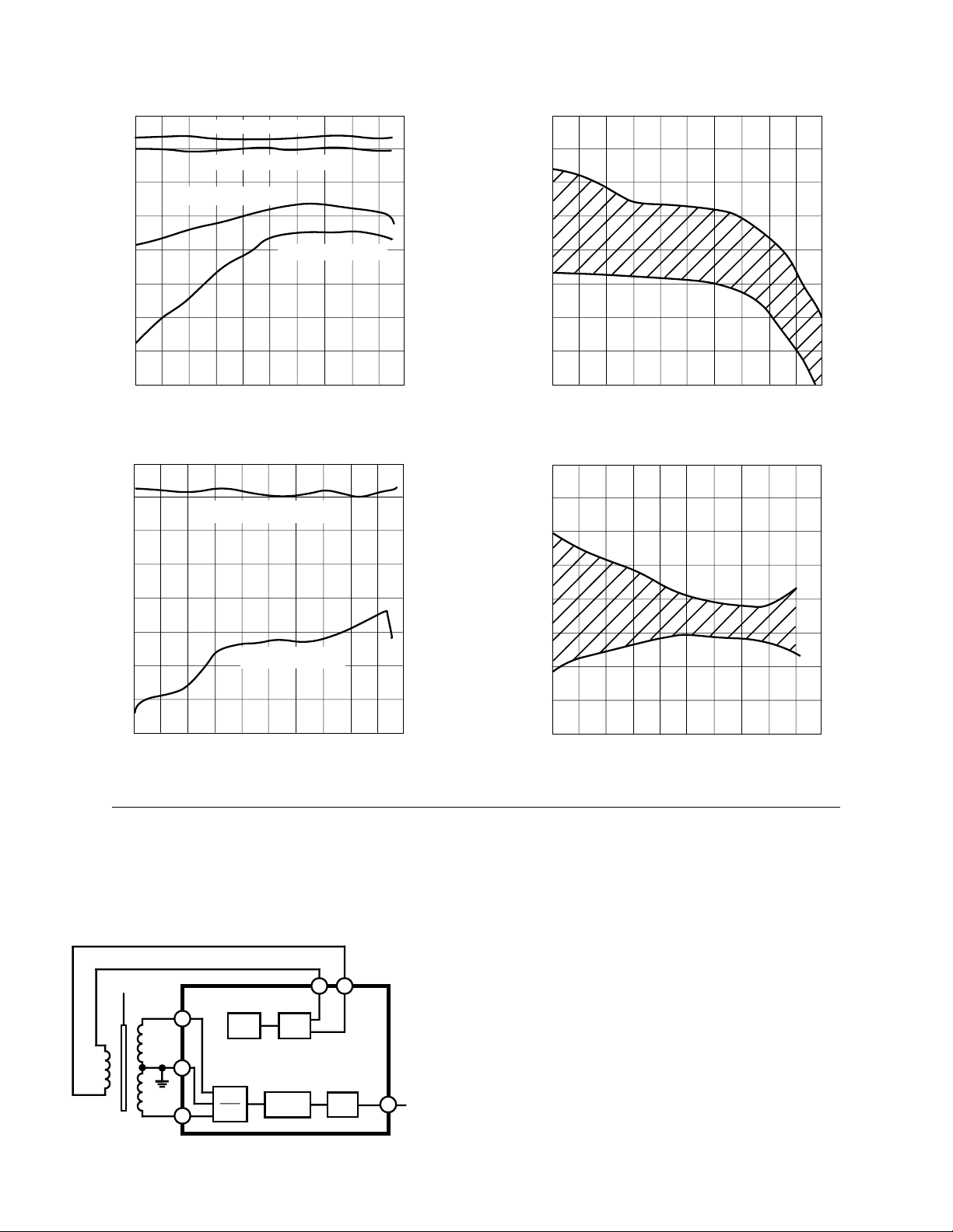
AD598–Typical Characteristics
–20 0 20 60 100 140–60
–10
–20
0
10
20
TEMPERATURE – °C
TYPICAL OFFSET DRIFT – ppm/°C
(at +258C and VS = 615 V, unless otherwise noted)
40
0
–40
–80
–120
–160
–200
GAIN AND OFFSET PSRR – ppm/Volt
–240
OFFSET PSRR 12–15V
OFFSET PSRR 15–18V
GAIN PSRR 12–15V
GAIN PSRR 15–18V
–20 0 20 60 100 140–60
TEMPERATURE – °C
Figure 1. Gain and Offset PSRR vs. Temperature
5
0
–5
–10
OFFSET CMRR ± 3V
120
80
40
20
0
–20
–40
TYPICAL GAIN DRIFT – ppm/°C
–60
–80
–20 0 20 60 100 140–60
TEMPERATURE – °C
Figure 2. Typical Gain Drift vs. Temperature
–15
–20
–25
GAIN AND OFFSET CMRR – ppm/Volt
–30
–35
–20 0 20 60 100 140–60
Figure 3. Gain and Offset CMRR vs. Temperature
THEORY OF OPERATION
A block diagram of the AD598 along with an LVDT (Linear
Variable Differential Transformer) connected to its input is
shown in Figure 5. The LVDT is an electromechanical transducer whose input is the mechanical displacement of a core and
whose output is a pair of ac voltages proportional to core position. The transducer consists of a primary winding energized by
EXCITATION (CARRIER)
V
A
11
GAIN CMRR ± 3V
TEMPERATURE – °C
OSC
AMP
Figure 4. Typical Offset Drift vs. Temperature
an external sine wave reference source, two secondary windings
connected in series, and the moveable core to couple flux between the primary and secondary windings.
The AD598 energizes the LVDT primary, senses the LVDT
secondary output voltages and produces a dc output voltage
proportional to core position. The AD598 consists of a sine
wave oscillator and power amplifier to drive the primary, a decoder which determines the ratio of the difference between the
LVDT secondary voltages divided by their sum, a filter and an
23
output amplifier.
The oscillator comprises a multivibrator which produces a
triwave output. The triwave drives a sine shaper, which produces a low distortion sine wave whose frequency is determined
LVDT
17
A–B
A+B
10
V
B
FILTER
AD598
AMP
V
16
OUT
Figure 5. AD598 Functional Block Diagram
by a single capacitor. Output frequency can range from 20 Hz to
20 kHz and amplitude from 2 V rms to 24 V rms. Total harmonic distortion is typically –50 dB.
The output from the LVDT secondaries consists of a pair of
sine waves whose amplitude difference, (V
), is proportional
A–VB
to core position. Previous LVDT conditioners synchronously
detect this amplitude difference and convert its absolute value to
REV. A–4–
Page 5
AD598
a voltage proportional to position. This technique uses the primary excitation voltage as a phase reference to determine the
polarity of the output voltage. There are a number of problems
associated with this technique such as (1) producing a constant
amplitude, constant frequency excitation signal, (2) compensating
for LVDT primary to secondary phase shifts, and (3) compensating for these shifts as a function of temperature and frequency.
The AD598 eliminates all of these problems. The AD598 does
not require a constant amplitude because it works on the ratio of
the difference and sum of the LVDT output signals. A constant
frequency signal is not necessary because the inputs are rectified
and only the sine wave carrier magnitude is processed. There is
no sensitivity to phase shift between the primary excitation and
the LVDT outputs because synchronous detection is not employed. The ratiometric principle upon which the AD598 operates requires that the sum of the LVDT secondary voltages
remains constant with LVDT stroke length. Although LVDT
manufacturers generally do not specify the relationship between
V
and stroke length, it is recognized that some LVDTs do
A+VB
not meet this requirement. In these cases a nonlinearity will
result. However, the majority of available LVDTs do in fact
meet these requirements.
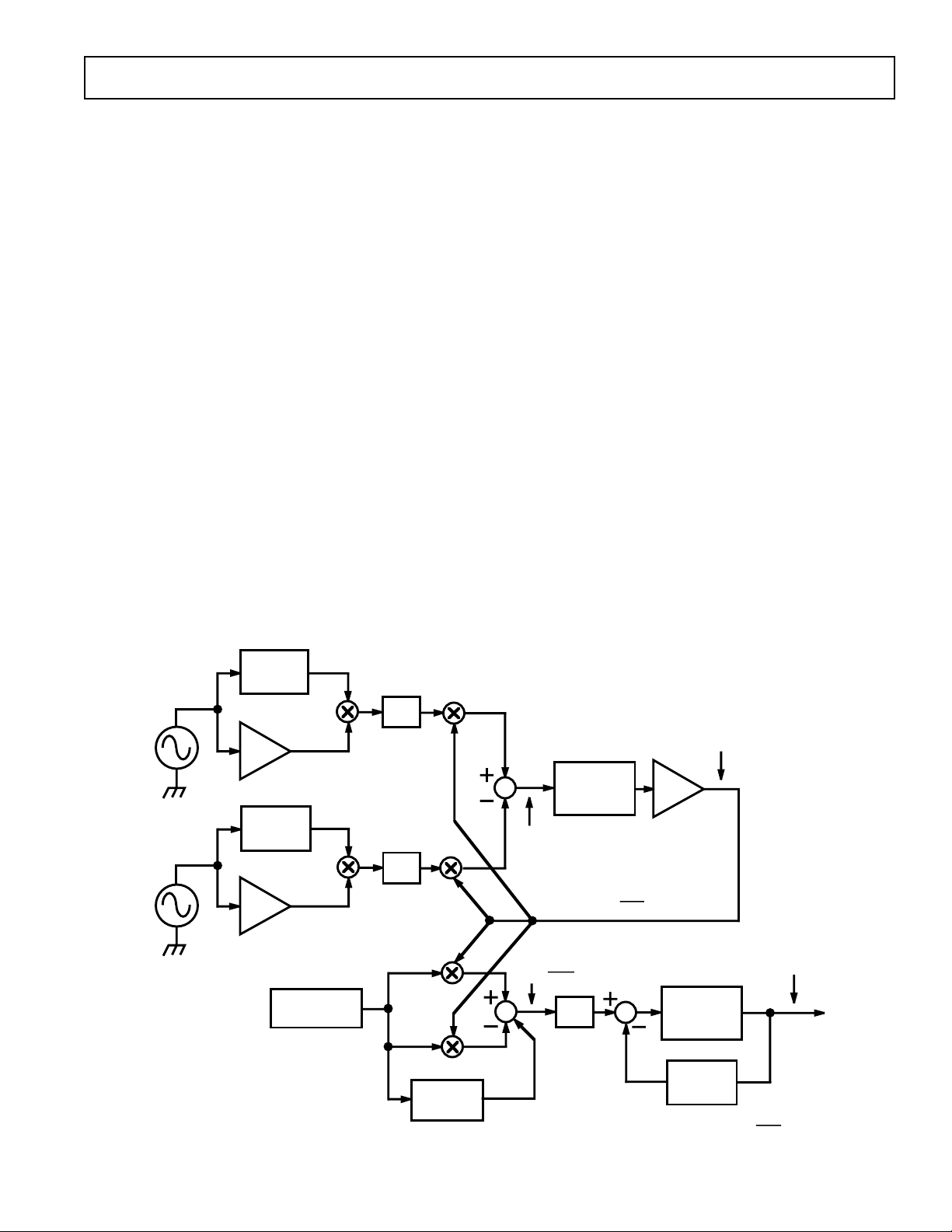
The AD598 utilizes a special decoder circuit. Referring to the
block diagram and Figure 6 below, an implicit analog computing loop is employed. After rectification, the A and B signals are
multiplied by complementary duty cycle signals, d and (I–d)
respectively. The difference of these processed signals is integrated and sampled by a comparator. It is the output of this
comparator that defines the original duty cycle, d, which is fed
back to the multipliers.
As shown in Figure 6, the input to the integrator is [(A+B)d]B.
Since the integrator input is forced to 0, the duty cycle d =
B/(A+B).
The output comparator which produces d = B/(A+B) also controls an output amplifier driven by a reference current. Duty
cycle signals d and (1–d) perform separate modulations on the
reference current as shown in Figure 6, which are summed. The
summed current, which is the output current, is I
× (1–2d).
REF
Since d = B/(A+B), by substitution the output current equals
I
× (A–B)/(A+B). This output current is then filtered and
REF
converted to a voltage since it is forced to flow through the scaling resistor R2 such that:
= I
V
OUT
×( A– B)/(A+ B)× R2
REF
CONNECTING THE AD598
The AD598 can easily be connected for dual or single supply
operation as shown in Figures 7 and 12. The following general
design procedures demonstrate how external component values
are selected and can be used for any LVDT which meets AD598
input/output criteria.
Parameters which are set with external passive components include: excitation frequency and amplitude, AD598 system
bandwidth, and the scale factor (V/inch). Additionally, there are
optional features, offset null adjustment, filtering, and signal integration which can be used by adding external components.
INPUT
INPUT
V TO I
COMP
V TO I
COMP
±1
±1
BANDGAP
REFERENCE
FILT
FILT
I
REF
A
B
d
RTO
OFFSET
d
1–d
1–d
∑
(A+B) d–B
I
REF
∑
●
A–B
A+B
INTEG
FILT
BINARY SIGNAL
0<d<1
B
●
d
A+B
∑
V
= R
OUT
d - DUTY CYCLE
COMP
INTEG
V TO I
SCALE
x I
REF
x
A–B
A+B
VOLTS
OUTPUT
REV. A
Figure 6. Block Diagram of Decoder
–5–
Page 6

AD598
DESIGN PROCEDURE DUAL SUPPLY OPERATION
Figure 7 shows the connection method with dual ±15 volt power
supplies and a Schaevitz E100 LVDT. This design procedure
can be used to select component values for other LVDTs as
well. The procedure is outlined in Steps 1 through 10 as follows:
1. Determine the mechanical bandwidth required for LVDT
position measurement subsystem, f
example, assume f
SUBSYSTEM
SUBSYSTEM
= 250 Hz.
. For this
2. Select minimum LVDT excitation frequency, approximately
10 × f
SUBSYSTEM
. Therefore, let excitation frequency = 2.5 kHz.
3. Select a suitable LVDT that will operate with an excitation
frequency of 2.5 kHz. The Schaevitz E100, for instance, will
operate over a range of 50 Hz to 10 kHz and is an eligible
candidate for this example.
4. Determine the sum of LVDT secondary voltages V
Energize the LVDT at its typical drive level V
and VB.
A
as shown in
PRI
the manufacturer’s data sheet (3 V rms for the E100). Set the
core displacement to its center position where V
sure these values and compute their sum V
E100, V
= 2.70 V rms. This calculation will be used
A+VB
A+VB
= VB. Mea-
A
. For the
later in determining AD598 output voltage.
5. Determine optimum LVDT excitation voltage, V
the LVDT energized at its typical drive level V
EXC
, set the
PRI
. With
core displacement to its mechanical full-scale position and
measure the output V
of whichever secondary produces
SEC
the largest signal. Compute LVDT voltage transformation
ratio, VTR.
For the E100, V
VTR = V
= 1.71 V rms for V
SEC
PRI/VSEC
= 3 V rms.
PRI
VTR = 1.75.
The AD598 signal input, V
, should be in the range of
SEC
1 V rms to 3.5 V rms for maximum AD598 linearity and
minimum noise susceptibility. Select V
fore, LVDT excitation voltage V
= V
V
EXC
× VTR = 3 × 1.75 = 5.25 V rms
SEC
EXC
= 3 V rms. There-
SEC
should be:
Check the power supply voltages by verifying that the peak
values of V
ages at +V
6. Referring to Figure 7, for V
and VB are at least 2.5 volts less than the volt-
A
and –VS.
S
= ±15 V, select the value of the
S
amplitude determining component R1 as shown by the curve
in Figure 8.
7. Select excitation frequency determining component C1.
30
20
rms
V
–
EXC
V
10
0
0.01 0.1
C1 = 35
µ
F Hz/f
1
R1 – kΩ
EXCITATION
V
rms
10 100 1000
+
15V
–15V
SCHAEVITZ E100
LVDT
Figure 8. Excitation Voltage V
6.8µF 0.1µF
0.1µF6.8µF
+V
A1 FILT
A2 FILT
20
S
R4
19
C4
C3
SIGNAL
REFERENCE
R
L
V
OUT
NOTE
FOR C1, C2, C3 AND C4 MYLAR
CAPACITORS ARE
RECOMMENDED. CERAMIC
CAPACITORS MAY BE
SUBSTITUTED. FOR R2, R3 AND
R4 USE STANDARD 1%
RESISTORS.
18
R3
17
16
15
14
13
12
V
A
R2
1
–V
S
2
EXC 1
3
EXC 2
4
R1
C1
C2
V
B
V
A
LEV 1
5
LEV 2
6
FREQ 1
7
FREQ 2
8
B1 FILT
9
B2 FILT
10 11
V
B
OFFSET 1
OFFSET 2
SIG REF
SIG OUT
FEEDBACK
OUT FILT
AD598
EXC
vs. R1
Figure 7. Interconnection Diagram for Dual Supply Operation
–6–
REV. A
Page 7

AD598
+
5
+
0.1 d0.1
–
5
–
(INCHES)
V
OUT
(
VOLTS)
+
10
0.1
–
+
0.1 d
+
5
(INCHES)
V
OUT
(
VOLTS)
8. C2, C3 and C4 are a function of the desired bandwidth of
the AD598 position measurement subsystem. They should
be nominally equal values.
C2 = C3 = C4 = 10
–4
Farad Hz/f
SUBSYSTEM
(Hz)
If the desired system bandwidth is 250 Hz, then
–4
C2 = C3 = C4 = 10
Farad Hz/250 Hz = 0.4 µF
See Figures 13, 14 and 15 for more information about
AD598 bandwidth and phase characterization.
9. In order to Compute R2, which sets the AD598 gain or fullscale output range, several pieces of information are needed:
a. LVDT sensitivity, S
b. Full-scale core displacement, d
c. Ratio of manufacturer recommended primary drive level,
V
to (VA + VB) computed in Step 4.
PRI
LVDT sensitivity is listed in the LVDT manufacturer’s catalog and has units of millivolts output per volts input per inch
displacement. The E100 has a sensitivity of 2.4 mV/V/mil.
In the event that LVDT sensitivity is not given by the manufacturer, it can be computed. See section on Determining
LVDT Sensitivity.
For a full-scale displacement of d inches, voltage out of the
AD598 is computed as
For no offset adjustment R3 and R4 should be open circuit.
To design a circuit producing a 0 V to +10 V output for a
displacement of ±0.1 inch, set V
to +10 V, d = 0.2 inch
OUT
and solve Equation (1) for R2.
R2 = 37.6 k
Ω
This will produce a response shown in Figure 10.
Figure 10. V
vs. Core Displacement (
(±5 V Full Scale)
OUT
±
0.1 Inch)
In Equation (2) set VOS = 5 V and solve for R3 and R4.
Since a positive offset is desired, let R4 be open circuit.
Rearranging Equation (2) and solving for R3
1. 2 × R 2
R3 =
–5kΩ=4.02 kΩ
V
OS
Figure 11 shows the desired response.
= S ×
(VA+VB)
V
OUT
V
is measured with respect to the signal reference,
OUT
PRI
×500 µA × R2 ×d.
V
Pin 17 shown in Figure 7.
Solving for R2,
×(VA+V
V
R2 =
Note that V
PRI
determine (V
For V
= 20 V full-scale range (±10 V) and d = 0.2 inch
OUT
A
OUT
S ×V
×500 µA ×d
PRI
is the same signal level used in Step 4 to
+ VB).
full-scale displacement (± 0.1 inch),
R2 =
V
as a function of displacement for the above example is
OUT
20V × 2. 70 V
2. 4 × 3 × 500 µA ×0.2
shown in Figure 9.
(
VOLTS)
V
OUT
+
10
–
Figure 9. V
–
10
OUT
+
(±10 V Full Scale)
vs. Core Displacement (
0.1 d0.1
)
B
= 75.3 kΩ
(INCHES)
±
0.1 Inch)
(1)
DESIGN PROCEDURE SINGLE SUPPLY OPERATION
Figure 12 shows the single supply connection method.
For single supply operation, repeat Steps 1 through 10 of the
design procedure for dual supply operation, then complete the
additional Steps 11 through 14 below. R5, R6 and C5 are additional component values to be determined. V
with respect to SIGNAL REFERENCE.
11. Compute a maximum value of R5 and R6 based upon the
12. The voltage drop across R5 must be greater than
10. Selections of R3 and R4 permit a positive or negative output
voltage offset adjustment.
1
VOS=1. 2 V × R 2 ×
*These values have a ±20% tolerance.
R 3 + 5 k Ω*
–
R 4 + 5 k Ω*
1
(2)
REV. A
R5≥
–7–
Figure 11. V
vs. Displacement (
relationship
2 +10 kΩ*
R 4 + 5 k Ω
Therefore
2+10 kΩ*
*These values have ±20% tolerance.
R4+ 5kΩ
Based upon the constraints of R5 + R6 (Step 11) and R5
(Step 12), select an interim value of R6.
(0 V–10 V Full Scale)
OUT
±
0.1 Inch)
R5 + R6 ≤ V
1. 2 V
1. 2 V
/100 µA
PS
+ 250 µA +
+250 µA+
100 µA
OUT
V
OUT
4 ×R2
V
OUT
4 ×R2
is measured
Volts
Ohms
Page 8

AD598
13. Load current through RL returns to the junction of R5 and
R6, and flows back to V
. Under maximum load condi-
PS
tions, make sure the voltage drop across R5 is met as
defined in Step 12.
As a final check on the power supply voltages, verify that the
peak values of V
voltages at +V
and VB are at least 2.5 volts less than the
A
and –VS.
S
14. C5 is a bypass capacitor in the range of 0.1 µF to 1 µF.
+
30V
15nF
V
B
R5
R6C5
+V
OFFSET 1
SIG REF
SIG OUT
OUT FILT
A1 FILT
A2 FILT
20
S
R4
19
R2
33k
C4
C3
SIGNAL
REFERENCE
R
L
V
OUT
18
R3
17
16
15
14
13
12
V
A
1
–V
S
2
EXC 1
3
EXC 2
4
R1
C1
C2
LEV 1
5
LEV 2
6
FREQ 1
7
FREQ 2
8
B1 FILT
9
B2 FILT
10 11
OFFSET 2
FEEDBACK
V
AD598
B
V
ps
0.1µF6.8µF
equal in value. Note also a shunt capacitor across R2 shown as a
parameter (see Figure 7). The value of R2 used was 81 kΩ with
a Schaevitz E100 LVDT.
V
SCHAEVITZ E100
LVDT
A
Figure 12. Interconnection Diagram for Single
Supply Operation
Gain Phase Characteristics
To use an LVDT in a closed loop mechanical servo application,
it is necessary to know the dynamic characteristics of the transducer and interface elements. The transducer itself is very quick
to respond once the core is moved. The dynamics arise primarily from the interface electronics. Figures 13, 14 and 15 show
the frequency response of the AD598 LVDT Signal Conditioner. Note that Figures 14 and 15 are basically the same; the
difference is frequency range covered. Figure 14 shows a wider
range of mechanical input frequencies at the expense of accuracy. Figure 15 shows a more limited frequency range with enhanced accuracy. The figures are transfer functions with the
input to be considered as a sinusoidally varying mechanical position and the output as the voltage from the AD598; the units of
the transfer function are volts per inch. The value of C2, C3 and
C4, from Figure 7, are all equal and designated as a parameter
in the figures. The response is approximately that of two real
poles. However, there is appreciable excess phase at higher frequencies. An additional pole of filtering can be introduced with
a shunt capacitor across R2, (see Figure 7); this will also increase phase lag.
When selecting values of C2, C3 and C4 to set the bandwidth of
the system, a trade-off is involved. There is ripple on the “dc”
position output voltage, and the magnitude is determined by the
filter capacitors. Generally, smaller capacitors will give higher
system bandwidth and larger ripple. Figures 16 and 17 show the
magnitude of ripple as a function of C2, C3 and C4, again all
Figure 13. Gain and Phase Characteristics vs. Frequency
(0 kHz–10 kHz)
Figure 14. Gain and Phase Characteristics vs. Frequency
(0 kHz–50 kHz)
–8–
REV. A
Page 9

Figure 15. Gain and Phase Characteristics vs. Frequency
1000
100
10
1
0.1
0.001 0.01 0.1
110
C2, C3, C4; C2 = C3 = C4 – µF
RIPPLE – mV rms
10kHz , C
SHUNT
= 0nF
10kHz , C
SHUNT
= 1nF
10kHz , C
SHUNT
= 10nF
(0 kHz–10 kHz)
1000
100
10
AD598
Figure 17. Output Voltage Ripple vs. Filter Capacitance
Determining LVDT Sensitivity
LVDT sensitivity can be determined by measuring the LVDT
secondary voltages as a function of primary drive and core position, and performing a simple computation.
Energize the LVDT at its recommended primary drive level,
V
(3 V rms for the E100). Set the core to midpoint where
PRI
V
= VB. Set the core displacement to its mechanical full-scale
A
position and measure secondary voltages V
(at Full Scale )–VB(at Full Scale )
V
Sensitivity =
From Figure 18,
Sensitivity =
A
V
SEC
1. 71 – 0.99
3 ×100 mils
WHEN V
PRI
V
PRI
= 3V rms
and VB.
A
×d
= 2. 4 mV/V/mil
V
A
1.71V rms
RIPPLE – mV rms
0.1
Figure 16. Output Voltage Ripple vs. Filter Capacitance
REV. A
1
0.01 0.1
C2, C3, C4; C2 = C3 = C4 – µF
1
2.5kHz, C
2.5kHz, C
2.5kHz, C
SHUNT
SHUNT
SHUNT
= 0nF
= 1nF
=10nF
0.99V rms
V
B
d = –100 mils d = 0
10
Figure 18. LVDT Secondary Voltage vs. Core Displacement
d =
+
100 mils
Thermal Shutdown and Loading Considerations
The AD598 is protected by a thermal overload circuit. If the die
temperature reaches 165°C, the sine wave excitation amplitude
gradually reduces, thereby lowering the internal power dissipation and temperature.
Due to the ratiometric operation of the decoder circuit, only
small errors result from the reduction of the excitation amplitude. Under these conditions the signal-processing section of
the AD598 continues to meet its output specifications.
The thermal load depends upon the voltage and current delivered to the load as well as the power supply potentials. An
LVDT Primary will present an inductive load to the sine wave
excitation. The phase angle between the excitation voltage and
current must also be considered, further complicating thermal
calculations.
–9–
Page 10

AD598–Applications
PROVING RING-WEIGH SCALE
Figure 20 shows an elastic member (steel proving ring) combined with an LVDT to provide a means of measuring very
small loads. Figure 19 shows the electrical circuit details.
The advantage of using a Proving Ring in combination with an
LVDT is that no friction is involved between the core and the
coils of the LVDT. This means that weights can be measured
without confusion from frictional forces. This is especially important for very low full-scale weight applications.
+
15V
6.8µF 0.1µF
0.1µF6.8µF
+V
–15V
0.015µF
0.1µF
V
SCHAEVITZ HR050
V
LVDT
–V
1
2
EXC 1
3
EXC 2
4
LEV 1
5
LEV 2
6
FREQ 1
C1
7
FREQ 2
8
C2
B
A
B1 FILT
9
B2 FILT
10 11
V
S
FEEDBACK
AD598
B
OFFSET 1
OFFSET 2
SIG REF
SIG OUT
OUT FILT
A1 FILT
A2 FILT
20
S
19
10k
SIGNAL
REFERENCE
R
L
V
OUT
18
17
16
1µF
15
14
13
12
V
A
C4
0.33µF
C3
0.1µF
634k
Figure 19. Proving Ring-Weigh Scale Circuit
FORCE/LOAD
PROVING
RING
LVDTCORE
Figure 20. Proving Ring-Weigh Scale Cross Section
Although it is recognized that this type of measurement system
may best be applied to weigh very small weights, this circuit was
designed to give a full-scale output of 10 V for a 500 lb weight,
using a Morehouse Instruments model 5BT Proving Ring. The
LVDT is a Schaevitz type HR050 (±50 mil full scale). Although
this LVDT provides ±50 mil full scale, the value of R2 was calculated for d = ±30 mil and V
equal to 10 V as in Step 9 of
OUT
the design procedures.
The 1 µF capacitor provides extra filtering, which reduces noise
induced by mechanical vibrations. The other circuit values were
calculated in the usual manner using the design procedures.
This weigh-scale can be designed to measure tare weight simply
by putting in an offset voltage by selecting either R3 or R4 (as
shown in Figures 7 and 12). Tare weight is the weight of a container that is deducted from the gross weight to obtain the net
weight.
The value of R3 or R4 can be calculated using one of two separate methods. First, a potentiometer may be connected between
Pins 18 and 19 of the AD598, with the wiper connected to
–V
. This gives a small offset of either polarity; and the
SUPPLY
value can be calculated using Step 10 of the design procedures.
For a large offset in one direction, replace either R3 or R4 with
a potentiometer with its wiper connected to –V
SUPPLY
.
The resolution of this weigh-scale was checked by placing a 100
gram weight on the scale and observing the AD598 output signal deflection on an oscilloscope. The deflection was 4.8 mV.
The smallest signal deflection which could be measured on the
oscilloscope was 450 µV which corresponds to a 10 gram
weight. This 450 µV signal corresponds to an LVDT displace-
ment of 1.32 microinches which is equivalent to one tenth of the
wave length of blue light.
The Proving Ring used in this circuit has a temperature coefficient of 250 ppm/°C due to Young’s Modulus of steel. By putting a resistor with a temperature coefficient in place of R2 it is
possible to temperature compensate the weigh-scale. Since the
steel of the Proving Ring gets softer at higher temperatures, the
deflection for a given force is larger, so a resistor with a negative
temperature coefficient is required.
SYNCHRONOUS OPERATION OF MULTIPLE LVDTS
In many applications, such as multiple gaging measurement, a
large number of LVDTs are used in close physical proximity. If
these LVDTs are operated at similar carrier frequencies, stray
magnetic coupling could cause beat notes to be generated. The
resulting beat notes would interfere with the accuracy of measurements made under these conditions. To avoid this situation
all the LVDTs are operated synchronously.
The circuit shown in Figure 21 has one master oscillator and
any number of slaves. The master AD598 oscillator has its frequency and amplitude programmed in the usual manner via R1
and C2 using Steps 6 and 7 in the design procedures. The slave
AD598s all have Pins 6 and 7 connected together to disable
their internal oscillators. Pins 4 and 5 of each slave are connected to Pins 2 and 3 of the master via 15 kΩ resistors, thus
setting the amplitudes of the slaves equal to the amplitude of the
master. If a different amplitude is required the 15 kΩ resistor
values should be changed. Note that the amplitude scales linearly with the resistor value. The 15 kΩ value was selected because it matches the nominal value of resistors internal to the
circuit. Tolerances of 20% between the slave amplitudes arise
due to differing internal resistors values, but this does not affect
the operation of the circuit.
Note that each LVDT primary is driven from its own power amplifier and thus the thermal load is shared between the AD598s.
There is virtually no limit on the number of slaves in this circuit,
since each slave presents a 30 kΩ load to the master AD598
power amplifier. For a very large number of slaves (say 100 or
more) one may need to consider the maximum output current
drawn from the master AD598 power amplifier.
–10–
REV. A
Page 11

AD598
–
0.015µF
0.1µF
V
MASTER SLAVE 1 SLAVE 2
1
–V
S
2
EXC 1
3
EXC 2
4
LEV 1
5
LEV 2
6
FREQ 1
7
FREQ 2
8
B1 FILT
9
B2 FILT
10 11
V
OFFSET 1
OFFSET 2
SIG REF
SIG OUT
FEEDBACK
OUT FILT
A1 FILT
A2 FILT
AD598
B
SCHAEVITZ E 100
MECHANICAL POSITION INPUT
+
V
+V
20
S
19
18
17
82.5kΩ
16
15
14
13
12
V
A
LVDT LVDT LVDT
15k 15k
0.33µF
0.1µF
–
V
1
–V
2
EXC 1
3
EXC 2
4
LEV 1
5
LEV 2
6
FREQ 1
7
FREQ 2
8
0.1µF
B1 FILT
9
B2 FILT
10 11
V
B
S
FEEDBACK
AD598
SCHAEVITZ E 100
MECHANICAL POSITION INPUT
Figure 21. Multiple LVDTs—Synchronous Operation
HIGH RESOLUTION POSITION-TO-FREQUENCY CIRCUIT
In the circuit shown in Figure 22, the AD598 is combined with
an AD652 voltage-to-frequency (V/F) converter to produce an
effective, simple data converter which can make high resolution
measurements.
This circuit transfers the signal from the LVDT to the V/F converter in the form of a current, thus eliminating the errors normally caused by the offset voltage of the V/F converter. The V/F
converter offset voltage is normally the largest source of error in
–
V
1
–V
2
EXC 1
3
EXC 2
4
LEV 1
5
LEV 2
6
FREQ 1
7
FREQ 2
8
0.1µF
B1 FILT
9
B2 FILT
10 11
V
+
V
+V
20
OFFSET 1
OFFSET 2
SIG REF
SIG OUT
FEEDBACK
OUT FILT
A1 FILT
A2 FILT
S
19
18
17
82.5kΩ
16
15
14
13
12
V
A
S
AD598
B
SCHAEVITZ E 100
MECHANICAL POSITION INPUT
0.33µF
0.1µF
+V
OFFSET 1
OFFSET 2
SIG REF
SIG OUT
OUT FILT
A1 FILT
A2 FILT
+
V
20
S
19
18
17
82.5kΩ
16
15
14
13
12
V
A
15k 15k
0.33µF
0.1µF
such circuits. The analog input signal to the AD652 is converted
to digital frequency output pulses which can be counted by
simple digital means.
This circuit is particularly useful if there is a large degree of
mechanical vibration (hum) on the position to be measured.
The hum may be completely rejected by counting the digital frequency pulses over a gate time (fixed period) equal to a multiple
of the hum period. For the effects of the hum to be completely
rejected, the hum must be a periodic signal.
–
Vs
0.1µF
1
–V
S
2
EXC 1
3
EXC 2
4
LEV 1
5
0.015µF
LEV 2
6
FREQ 1
7
FREQ 2
8
B1 FILT
9
B2 FILT
0.1µF
10 11
V
B
SCHAEVITZ E 100
MECHANICAL POSITION INPUT
GND
OFFSET 1
OFFSET 2
FEEDBACK
OUT FILT
AD598
+V
SIG REF
SIG OUT
A1 FILT
A2 FILT
0.1µF
S
V
A
20
19
18
17
16
15
14
13
12
LVDT
+
Vs
+V
1
S
2
TRIM
TRIM
3
OP AMP OUT
4
AD652
SYNCHRONOUS
VOLTAGE TO
FREQUENCY
CONVERTER
COMP REF
COMP“+”
COMP“–”
ANALOG GND
16
15
14
13
0.02µF
12
2.5k
+V
CK
FREQ
OUT
S
11
10
500KHZ
9
C
OS
+V
S
0.33µF
0.1µF
OP AMP “–”
5
OP AMP “+”
6
7
10 VOLT INPUT
8
–V
S
DIGITAL GND
FREQ OUT
CLOCK INPUT
REV. A
Figure 22. High Resolution Position-to-Frequency Converter
–11–
Page 12

AD598
The V/F converter is currently set up for unipolar operation.
The AD652 data sheet explains how to set up for bipolar operation. Note that when the LVDT core is centered, the output frequency is zero. When the LVDT core is positioned off center,
and to one side, the frequency increases to a full-scale value.
To introduce bipolar operation to this circuit, an offset must be
introduced at the LVDT as shown in Step 10 of the design
procedures.
LOW COST SET-POINT CONTROLLER
A low cost set-point controller can be implemented with the circuit shown in Figure 23. Such a circuit could possibly be used
in automobile fuel control systems. The potentiometer, P1, is
attached to the gas pedal, and the LVDT is attached to the butterfly valve of the fuel injection system or carburetor. The position of the butterfly valve is electronically controlled by the
position of the gas pedal, without mechanical linkage.
This circuit is a simple two IC closed loop servo-controller. It is
simple because the LVDT circuit is functioning as the loop integrator. By putting a capacitor in the feedback path (normally occupied by R2), the output signal from the AD598 corresponds
to the time integral of the position being measured by the
LVDT. The LVDT position signal is summed with the offset
signal introduced by the potentiometer, P1. Since this sum is integrated, it must be forced to zero. Thus the LVDT position is
forced to follow the value of the input potentiometer, P1. The
output signal from the AD598 drives the LM675 power amplifier, which in turn drives the solenoid.
This circuit has dual advantages of being both low cost and high
accuracy. The high accuracy results from avoiding the offset errors normally associated with converting the LVDT signal to a
voltage and then subsequently integrating that voltage.
MECHANICAL FOLLOWER SERVO-LOOP
Figure 24 shows how two Schaevitz E100 LVDTs may be combined with two AD598s in a mechanical follower servo-loop
configuration. One of the LVDTs provides the mechanical input
position signal, while the other LVDT mimics the motion.
The signal from the input position circuit is fed to the output as
a current so that voltage offset errors are avoided. This current
signal is summed with the signal from the output position
LVDT; this summed signal is integrated such that the output
position is now equal to the input position. This circuit is an
efficient means of implementing a mechanical servo-loop since
only three ICs are required.
This circuit is similar to the previous circuit (Figure 23) with
one exception: the previous circuit uses a potentiometer instead
of an LVDT to provide the input position signal. Replacing the
potentiometer with an LVDT offers two advantages. First, the
increased reliability and robustness of the LVDT can be exploited in applications where the position input sensor is located
in a hostile environment. Second, the mechanical motions of the
input and output LVDTs are guaranteed to be identical to
within the matching of their individual scale factors. These
particular advantages make this circuit ideal for application as a
hydraulic actuator controller.
DIFFERENTIAL GAGING
LVDTs are commonly used in gaging systems. Two LVDTs
can be used to measure the thickness or taper of an object. To
measure thickness, the LVDTs are placed on either side of the
object to be measured. The LVDTs are positioned such that
there is a known maximum distance between them in the fully
retracted position.
This circuit is both simple and inexpensive. It has the advantage
that two LVDTs may be driven from one AD598, but the disadvantage is that the scale factor of each LVDT may not match
exactly. This causes the workpiece thickness measurement to
vary depending upon its absolute position in the differential
gage head.
This circuit was designed to produce a ±10 V signal output
swing, composed of the sum of the two independent ±5 V
swings from each LVDT. The output voltage swing is set with
an 80.9 kΩ resistor. The output voltage V
for this circuit is
OUT
given by:
V
OUT
(V
A–VB
=
(V
A+VB
(V
)
+
)
(V
C–VD
C+VD
)
×500 µA × R2.
)
INPUT
MECHANICAL
POSITION
OUTPUT
POSITION
SCHAEVITZ E 100
LVDT
0.015µF
0.1µF
MASS ON SPRING
620 N/m
33 GRAMS
0.1µF
1
–V
S
2
EXC 1
3
EXC 2
4
LEV 1
5
LEV 2
6
FREQ 1
7
FREQ 2
8
B1 FILT
9
B2 FILT
10 11
V
AD598
B
+V
OFFSET 1
OFFSET 2
SIG REF
SIG OUT
FEEDBACK
OUT FILT
A1 FILT
A2 FILT
+
V
INPUT PI
20
S
19
18
17
16
15
14
13
12
V
A
0.33µF
0.1µF
50kΩ
30k
1µF
0.01µF
Figure 23. Low Cost Set-Point Controller
–12–
100Ω
10k
0.068µF
49.9k
0.33µF
IN4740A
10V
1000pF
150k
+
V
LM675
4.99k
+
V
20k 47µF
POWER SUPPLY
0.1µF
GUARDIAN SOLENOID
12 VDC 2–INT–12D
62 CONE
+
25V
33µF
47µF
GND
REV. A
Page 13

AD598
EXC 1
EXC 2
LEV 1
LEV 2
FREQ 1
FREQ 2
B1 FILT
B2 FILT
OFFSET 1
OFFSET 2
SIG REF
SIG OUT
FEEDBACK
OUT FILT
A1 FILT
A2 FILT
AD598
0.1µF
–V
S
+V
S
1
2
3
4
5
6
7
8
9
10 11
12
13
14
16
15
17
18
19
20
V
B
V
A
+
V
0.015µF
0.1µF
0.1µF
0.33µF
0.01µF
1µF
30k
OUTPUT
MECHANICAL
POSITION
SCHAEVITZ E 100
LVDT
100Ω
10k
0.33µF
1000pF
150k
0.1µF
+
V
MASS ON SPRING
620 N/m
33 GRAMS
0.068µF
49.9k
4.99k
20k 47µF
47µF
33µF
+
25V
GND
POWER SUPPLY
+
V
LM675
EXC 1
EXC 2
LEV 1
LEV 2
FREQ 1
FREQ 2
B1 FILT
B2 FILT
OFFSET 1
OFFSET 2
SIG REF
SIG OUT
FEEDBACK
OUT FILT
A1 FILT
A2 FILT
AD598
0.1µF
–V
S
+V
S
1
2
3
4
5
6
7
8
9
10 11
12
13
14
16
15
17
18
19
20
V
B
V
A
+
V
0.015µF
0.1µF
0.1µF
0.33µF
INPUT
MECHANICAL
POSITION
SCHAEVITZ E 100
LVDT
4.99k
IN4740A
10V
GUARDIAN SOLENOID
12 VDC 2-INT-12D
62 CONE
REV. A
SCHAEVITZ E 100
SCHAEVITZ E 100
Figure 24. Mechanical Follower Servo-Loop
A
B
LVDT 1
C
D
LVDT 2
Figure 25. Differential Gaging
–13–
–
V
0.1µF 0.1µF
1
2
3
4
5
0.015µF
6
7
8
9
0.1µF
10 11
V
OUT
–V
S
EXC 1
EXC 2
LEV 1
LEV 2
FREQ 1
FREQ 2
B1 FILT
B2 FILT
V
B
(V
A–VB
=
A+VB
(V
FEEDBACK
AD598
)+(VC–VD)
)+(VC+VD)
+V
S
OFFSET 1
OFFSET 2
SIG REF
SIG OUT
OUT FILT
A1 FILT
A2 FILT
V
A
• 500µA • R2
+
V
20
19
18
17
16
R2
80.9kΩ
0.33µF
0.1µF
15
14
13
12
V
±
10V
OUT
FULL SCALE
Page 14

AD598
PRECISION DIFFERENTIAL GAGING
The circuit shown in Figure 26 is functionally similar to the differential gaging circuit shown in Figure 25. In contrast to Figure
25, it provides a means of independently adjusting the scale factor of each LVDT so that both scale factors may be matched.
The two LVDTs are driven in a master-slave arrangement
where the output signal from the slave LVDT is summed with
the output signal from the master LVDT. The scale factor of the
slave LVDT only is adjusted with R1 and R2. The summed
scale factor of the master LVDT and the slave LVDT is adjusted with R3.
15kΩ
15kΩ
A
B
MASTER LVDT
R1 and R2 are chosen to be 80.9 kΩ resistors to give a ± 10 V
full-scale output signal for a single Schaevitz E100 LVDT. R3 is
chosen to be 40.2 kΩ to give a ± 10 V output signal when the
two E100 LVDT output signals are summed. The output voltage for this circuit is given by:
(V
V
OUT
–
V
0.015µF
0.1µF
A–VB
=
(V
A+VB
0.1µF 0.1µF
1
–V
S
2
EXC 1
3
EXC 2
4
LEV 1
5
LEV 2
6
FREQ 1
7
FREQ 2
8
B1 FILT
9
B2 FILT
10 11
V
B
)
)
OFFSET 1
OFFSET 2
FEEDBACK
OUT FILT
AD598
(V
+
(V
SIG REF
SIG OUT
A1 FILT
A2 FILT
C–VD
C+VD
+V
20
S
19
18
17
16
15
14
13
12
V
A
)
R2
×
)
R1
+
V
R3 40.2kΩ
×500 µA × R3.
V
FULL SCALE
0.33µF
0.1µF
OUT
±
10V
SCHAEVITZ E 100
C
D
SLAVE
LVDT
–
V
0.1µF 0.1µF
1
–V
S
2
EXC 1
3
EXC 2
4
LEV 1
5
LEV 2
6
FREQ 1
7
FREQ 2
8
B1 FILT
9
0.1µF
B2 FILT
10 11
V
B
VA–V
V
=
OUT
VA+V
Figure 26. Precision Differential Gaging
OFFSET 1
OFFSET 2
FEEDBACK
OUT FILT
AD598
B
VC–V
+
B
VC+V
+V
SIG REF
SIG OUT
A1 FILT
A2 FILT
D
D
R1
+
V
20
S
19
18
17
16
15
14
13
12
V
A
R2
500µA
••
R1
•
0.33µF
0.1µF
R3
80.9kΩ
R2
80.9kΩ
–14–
REV. A
Page 15

AD598
OPERATION WITH A HALF-BRIDGE TRANSDUCER
Although the AD598 is not intended for use with a half-bridge
type transducer, it may be made to function with degraded
performance.
A half-bridge type transducer is a popular transducer. It works
in a similar manner to the LVDT in that two coils are wound
around a moveable core and the inductance of each coil is a
function of core position.
In the circuit shown in Figure 27 the V
and VB input voltages
A
are developed as two resistive-inductor dividers. If the inductors
are equal (i.e., the core is centered), the V
ages to the AD598 are equal and the output voltage V
and VB input volt-
A
OUT
is
zero. When the core is positioned off center, the inductors are
unequal and an output voltage V
is developed.
OUT
The linearity of this circuit is dependent upon the value of the
resistors in the resistive-inductor dividers. The optimum value
may be transducer dependent and therefore must be selected by
–
V
0.1µF 0.1µF
1
2
EXC 1
3
EXC 2
4
LEV 1
5kΩ
5
LEV 2
6
FREQ 1
7
FREQ 2
8
B1 FILT
9
B2 FILT
10 11
V
SANGAMO
AGHI
HALF-BRIDGE
MECHANICAL
POSITION
INPUT
1µF1µF
300Ω 300Ω
4nF
0.1µF
trial and error. The 300 Ω resistors in this circuit optimize the
nonlinearity of the transfer function to within several tenths of
1%. This circuit uses a Sangamo AGH1 half-bridge transducer.
The 1 µF capacitor blocks the dc offset of the excitation output
signal. The 4 nF capacitor sets the transducer excitation frequency to 10 kHz as recommended by the manufacturer.
ALTERNATE HALF-BRIDGE TRANSDUCER CIRCUIT
This circuit suffers from similar accuracy problems to those
mentioned in the previous circuit description. In this circuit the
V
input signal to the AD598 really and truly is a linear function
A
of core position, and the input signal V
, is one half of the exci-
B
tation voltage level. However, a nonlinearity is introduced by
the A–B/A+B transfer function.
The 500 Ω resistors in this circuit are chosen to minimize errors
caused by dc bias currents from the V
and VB inputs. Note that
A
in the previous circuit these bias currents see very low resistance
paths to ground through the coils.
+
V
+V
SIG REF
A1 FILT
A2 FILT
20
S
19
18
17
16
15
14
13
12
V
A
82.5kΩ
0.33µF
0.1µF
±
V
10V
OUT
FULL SCALE
–V
S
OFFSET 1
OFFSET 2
SIG OUT
FEEDBACK
OUT FILT
AD598
B
REV. A
SANGAMO
AGHI
HALF-BRIDGE
MECHANICAL
POSITION
INPUT
1µF
Figure 27. Half-Bridge Operation
–
V
0.1µF 0.1µF
1
–V
S
OFFSET 1
OFFSET 2
SIG REF
SIG OUT
FEEDBACK
OUT FILT
A1 FILT
A2 FILT
AD598
500Ω
500Ω
1.87kΩ
4nF
0.1µF
2
EXC 1
3
EXC 2
4
LEV 1
5
LEV 2
6
FREQ 1
7
FREQ 2
8
B1 FILT
9
B2 FILT
10 11
V
B
Figure 28. Alternate Half-Bridge Circuit
–15–
+V
+
V
20
S
19
18
17
±
V
10V
16
15
14
13
12
V
A
143kΩ
0.33µF
0.1µF
OUT
FULL SCALE
Page 16

AD598
OUTLINE DIMENSIONS
Dimensions shown in inches and (mm).
20-Pin Sized Brazed Ceramic DIP
C1330–10–10/89
20-Lead Wide Body Plastic SOIC (R) Package
–16–
PRINTED IN U.S.A.
REV. A
 Loading...